Note : Les descriptions sont présentées dans la langue officielle dans laquelle elles ont été soumises.
CA 03053488 2019-08-13
WO 2018/152291 PCT/US2018/018310
RADIATION DETECTOR INCLUDING FIELD EFFECT TRANSISTOR IN
RESONANT CAVITY NANOSTRUCTURE
CROSS-REFERENCE TO RELATED APPLICATIONS
[0001] This application claims the benefit of U.S. Provisional Application
No. 62/459,538
filed February 15, 2017, the entire contents of which are incorporated by
reference herein.
TECHNICAL FIELD
[0002] The present disclosure relates to a radiation detector and to a
method of detection.
More particularly, the disclosure relates to a radiation detector and to a
method of detection
capable of identifying source material, radiation energy, and source
direction.
SUMMARY
[0003] Many radiation detectors operate based on a method requiring high
purity solid
crystals operating at extremely low temperatures and requiring high voltage
bias fields. Other
radiation detectors may use a secondary effect whereby incident radiation
causes a response in a
material, typically a scintillation of photon energy that is further detected
using photon receivers,
such as avalanche photofloods and photo multiplier tubes. The result is an
echo of the actual
event, allowing digital signal processing techniques to approximate the
probable cause of the
incident radiation event.
[0004] Conventional radiation testing methods that specifically involve
gamma and deep X-
ray energy are limited in both the range of sensitivity of incident energy and
the ability to
specifically isolate the probable source material within the sensitivity band.
Additionally, the
large crystal structure of the sensors inhibits pixelization for imaging
techniques. The large
structure of the existing technology further prohibits detection and recovery
necessary to capture
low energy and fast pulse events.
[0005] Some detector systems require cryo-cooling or liquid nitrogen to
operate efficiently,
require a high voltage source as an electron bias voltage to aid the
material's response, and/or
require a large detector material to insure proper cascading of charged
particles to generate a
1
CA 03053488 2019-08-13
WO 2018/152291 PCT/US2018/018310
response. Additionally, the power requirements of some detecting systems are
sufficiently high
such that the detectors have limited operation due to the size of the system
and batteries
necessary to power the detectors, cryo-pumps, and electronics. Furthermore,
the detection range
(e.g., the isotope detection range) of available sensors is limited to low
radiation environments
and narrow operating temperatures, such that a variety of detector probes may
be necessary to
provide a large spectrum of isotope sensing capability.
[0006] In one aspect, a radiation detection device includes a plurality of
field effect
transistors (FETs) arranged to form a resonant cavity. The cavity includes a
first end and a
second end, and the plurality of FETs provide an electromagnetic field
defining a standing wave
oscillating at a resonant frequency defined by a characteristic of the cavity.
A radiation input
passing through the cavity induces a perturbation of the electromagnetic
field.
[0007] In another aspect, a method of detecting radiation includes: tuning
a detector cavity to
be resonant with a frequency of radiation emitted by a target radiation
source; receiving an
incident radiation within the detector cavity; and detecting an incident
frequency of the incident
radiation.
[0008] In some aspects, the disclosure includes a detector and method
capable of high
resolution in an imaging array.
[0009] In some aspects, a gamma and/or neutron radiation detector does not
require special
environmental conditions, such as high voltage biasing and extremely low
operating
temperatures.
[0010] In some aspects, a gamma and/or neutron radiation detector requires
low power,
provides high sensitivity, and is actively tunable to filter out specific
isotope sources.
[0011] In some aspects, a single device includes an array of
electromagnetic radiation
detectors capable of parallel detection.
[0012] In some aspects, the disclosure includes a device and a method for
gamma and/or
neutron radiation detection including a THz resonant cavity structure.
2
CA 03053488 2019-08-13
WO 2018/152291 PCT/US2018/018310
[0013] Other aspects will become apparent by consideration of the detailed
description and
accompanying drawings.
BRIEF DESCRIPTION OF THE DRAWINGS
[0014] FIG.1 illustrates a long gate field effect transistor (FET), the
length of the gate being
designed to be resonant at the terahertz frequency unique to the desired
isotope's gamma
response.
[0015] FIG. 2 illustrates a mesa long gate FET structure. The surface of
the gate may be
contiguous and uniformly flat to accommodate the resonant tuning structure of
the long gate THz
receiver.
[0016] FIG. 3 illustrates a detector including multiple (e.g., six) long
gate THz receivers
arranged in a structure (e.g., a hexagon) to provide a tuned resonant cavity.
[0017] FIG. 4 illustrates a system of detectors arranged in an array of
resonant nano-cavities,
each including long gate THz receivers, as a two dimensional imaging array of
gamma detectors.
[0018] FIG. 5 schematically illustrates an optical coating deposited on a
surface of a THz
receiver structure for focusing incident gamma radiation along the surface of
the detector.
[0019] FIG. 6 illustrates a spherical optical concentration effect of a
gamma focusing coating
along a detector surface.
[0020] FIG. 7 illustrates an integrated nano-antenna for conducting
resonant cavity energy
from an incident gamma photon on a detector cavity and directing the energy to
a down-
converting Schottkey barrier detector-mixer diode structure built into a
cavity device
semiconductor.
[0021] FIG. 8 illustrates a spectrum for an array of n detectors. The
signal may be down
mixed to a manageable lower frequency to then be transmitted in parallel over
any connection
medium of the device (e.g., optical, radio frequency, using fiber, cable, or
wireless interface).
The frequency is tunable and may be selected such that the signal can be sent
from 1 to n
detectors simultaneously without interference. The down converting signals may
include, but are
3
CA 03053488 2019-08-13
WO 2018/152291 PCT/US2018/018310
not limited to, separate wavelengths for parallel transmission or single
wavelengths equal to each
other as a gamma-to-visible converter.
[0022] Before any embodiments are explained in detail, it is to be
understood that the
disclosure is not limited in its application to the details of construction
and the arrangement of
components set forth in the following description or illustrated in the
following drawings. The
disclosure is capable of other embodiments and of being practiced or of being
carried out in
various ways. Also, it is to be understood that the phraseology and
terminology used herein is for
the purpose of description and should not be regarded as limiting. Use of
"including" and
"comprising" and variations thereof as used herein is meant to encompass the
items listed
thereafter and equivalents thereof as well as additional items. Use of
"consisting of' and
variations thereof as used herein is meant to encompass only the items listed
thereafter and
equivalents thereof. Unless specified or limited otherwise, the terms
"mounted," "connected,"
"supported," and "coupled" and variations thereof are used broadly and
encompass both direct
and indirect mountings, connections, supports, and couplings.
DETAILED DESCRIPTION
[0023] Gamma radiation is a type of electromagnetic radiation having a
frequency greater
than about 1019 Hz (less than about 1011 m in wavelength). Conventional gamma
radiation
detection devices rely on either high purity crystals or gas ionization
detectors, both of which
suffer from low detection rates. In contrast, the disclosure relates to
detection devices and
methods having significantly greater sensitivity while reducing the need for
additional
electronics or processing to enhance signal detection. In some cases, the
disclosed detection
device and method can detect a single photon of gamma radiation.
[0024] FIGS. 1 and 2 illustrate a long gate field effect transistor (FET)
10 in which current
flow in a semiconductor between a source and a drain is controlled by applying
a bias voltage to
create an electric field.
[0025] FIG. 2 illustrates a mesa-type long gate FET structure, in which the
layers of an n-
and p-type semiconductor are built in a fashion to produce a uniform slab
rather than a stacked
device. The uniformly flat shape permits the FET device 10 to easily act as a
wall for a tuned
4
CA 03053488 2019-08-13
WO 2018/152291 PCT/US2018/018310
cavity, as described in further detail below. The surface of the FET gate may
be contiguous and
uniformly flat to accommodate a resonant tuning structure of a long gate THz
receiver, and to
minimize any surface perturbations that may interfere with the resonant cavity
feature. As
shown in FIG. 2, a FET substrate 12 may contain a piezoelectric material.
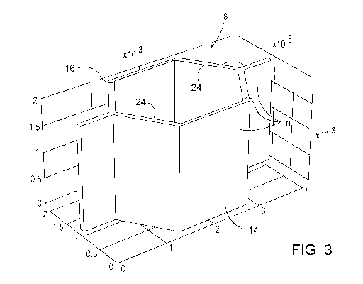
[0026] As shown in FIG. 3, a detector device 8 includes a plurality of FETs
10 arranged to
form a tube or cavity 16. The FET 10, as a structure defining a portion of the
cavity 16, is
sensitive to a standing wave caused by an electric field within the resonant
cavity 16, and the
field in the semiconductor fluctuates when a cavity frequency is perturbed
(e.g., by an input such
as a gamma particle). In some embodiments, the length of the gate is resonant
at the terahertz
frequency unique to a desired isotope's gamma response. The cavity length can
be equal to a
tuned harmonic of a desired target gamma frequency for detection.
[0027] In some embodiments, the length of the gate of the FET is adjustable
so that the
resonant frequency may be adjusted to a different isotope's gamma response. In
some
embodiments, the length of the gate may be continuously varied to scan across
a spectrum of
frequencies. The substrate 12 (FIG. 2) can be formed from a piezoelectric
material as part of the
detection device's substrate, allowing the length of the FET(s) 10 and
therefore the length of the
cavity 16 to change and thereby permitting a user to tune the resonant cavity
frequency. For
example, the device can be manufactured at any length necessary to allow the
device to act
within the bandwidth of the target electromagnetic field to be detected. In an
initial
configuration, the length of the cavity 10 can be tuned to selectively detect
gamma radiation
emitted from a first source material (e.g., plutonium (Pu)), and the length of
the cavity 16 can
then be adjusted to selectively detect gamma radiation emitted from a second
source material
(e.g., copper (Cu)).
[0028] FIG. 3 illustrates an exemplary embodiment of a detector including a
single cavity 16.
In the illustrated embodiment, the detector includes six long gate FETs acting
as THz receivers
and arranged to form a cavity 16 having a closed perimeter (e.g., a hexagonal
shape). In other
embodiments, the resonant cavity 16 may have a different structure and/or
shape (including, but
not limited to, a triangle, a square, a pentagon, etc.). In some embodiments,
a neutron-producing
coating 14 reacts to a neutron striking the surface by producing a response
gamma particle. The
CA 03053488 2019-08-13
WO 2018/152291 PCT/US2018/018310
gamma particle may pass through the cavity 16 and be detected. FIG. 3 also
illustrates the gated
surface of the hexagonal cavity 16. In a two-dimensional array topology, the
gate can be inside
or outside a resonant cavity structure due to the mesa construction of the FET
device. In the
illustrated embodiment, the cavity 16 includes pairs of parallel walls 24,
which facilitate
measuring time of flight (TOF) for incident gamma radiation by measuring a
difference in time
from an incident gamma photon striking one wall before exiting the cavity 16
through the
opposite wall.
[0029] The device may detect the radiation particle due to the particle's
disturbing or
perturbing electrons that group or collect at predetermined locations within
the resonant cavity
16. When the resonant cavity is stable (i.e., natural resonance), the
electromagnetic alternating
current wave is essentially sinusoidal in nature. The wave can become a
standing since wave
(FIG. 1), such that the peaks of the sine wave do not move along the length of
the cavity 16. The
cavity 16 is tuned to a specific frequency such that the resulting standing
wave is at or near
motionless relative to the length cavity 16. The wavelength of the resonant
frequency contains
multiple peak maximum energy points 18 (FIG. 1), representing the peak of the
electron resonant
sine wave within the cavity. Electrons 40 in the EM field group or collect
near the peak points,
as measured in a longitudinal direction along a length of the cavity 16. In
some embodiments,
the electrons in the EM field within the wave collect substantially within a
plane or disk
extending through the resonant cavity 16 and perpendicular to a longitudinal
axis of the cavity
16. Each plane or disk is located substantially at one of the peaks of the
standing resonant sine
wave. A space between these collections or groups of electrons can be
perceived as a distance
along a length of the cavity 16, and the distance between the groups of
electron is equal to the
resonant frequency wavelength of the cavity 16.
[0030] Incident photon or electromagnetic energy can cause a perturbation
via multiple
mechanisms. An incident electromagnetic field may directly cross through one
or more of the
electron field groups of the standing wave, causing a brief scattering. In
addition (or
alternatively), an incident electromagnetic wave may pass through a space
between the electron
groups, causing a space charge-related disturbance or perturbation of the
stable electron group.
Also, when incident gamma (or neutron) radiation crosses one of the long gate
THz receivers,
the radiation induces an oscillation in the standing wave of electrons, which
can be detected with
6
CA 03053488 2019-08-13
WO 2018/152291 PCT/US2018/018310
high sensitivity. The change in the standing wave causes a momentary loss or
addition of the
energy necessary to maintain the standing wave in balance in the cavity 16.
This loss or gain of
cavity energy causes electrons to flow into or out of the gate structure of
the FET 10, and the
resulting frequency disturbance of the FET device 10 (which is directly
proportional to the
energy of the incident electromagnetic field) is manifested as a mirror image
current in the FET
device 10. This current shift is detectable as both a current change and as a
shift in the resonant
frequency of the cavity 16, as the device naturally attempts to re-stabilize.
An analogous
reaction, for the purpose of illustration, is touching a plucked string: the
frequency shifts and
then attempts to regain a natural resonant point dictated by the length of the
string.
[0031] When incident radiation crosses two or more THz receivers, it may be
possible to
determine one or more of the properties of speed, energy, and/or direction of
the photon. Unlike
existing methods based solely on energy transductance of a gamma photon (which
requires the
incident photon to be stopped through collisions with the detector material),
the disclosed
method of detection relies only on the interaction of the radiation with a
high density of charged
particles, located within the electron groups of the resonant cavity 16. The
incident photon
merely needs to perturb the resonant field to for its presence to be detected.
[0032] As shown in FIG. 4, a system of multiple detectors 8 can be arranged
in an array 30
of resonant nano cavities 16, with each cavity 16 including long gate THz
receivers to form a
two-dimensional imaging array of gamma detectors. A substrate 34 of the plane
array 30 of
detector cavities 16 on a semiconductor structure may contain scanning row and
column
switches for translating the individual cavity signals into an image stream
for array detection.
The system can be positioned within a detector housing (not shown).
[0033] In certain embodiments, an array of resonant nano cavities is
configured to make an
image, analogous to a charged coupled device (CCD). In certain embodiments,
the array of
resonant nano cavities may be one-dimensional, two-dimensional, or three-
dimensional. The
array of nano cavities may include a plurality of detectors (e.g., numbered 1
to n). A three-
dimensional array can be formed by stacking two-dimensional arrays, each with
varying cavity
lengths such that a gamma photon incident along a perpendicular axis to the
array can be
detected in a wider resonant range. Incident gamma photons have very small
interaction cross
7
CA 03053488 2019-08-13
WO 2018/152291 PCT/US2018/018310
sections, so an array of small cavities increases the probability of
identifying the position along
the two-dimensional array where the gamma photon passes. Each resonant cavity
within the
array can represent an individual pixel of an imaging array, and the array is
sensitive to direct
conversion of gamma photons and indirect conversion of incident neutrons
(through the
detection of the gammas created when the neutron passes through one or more
walls of a
resonant cavity pixel).
[0034] A two-dimensional array of resonant cavity detectors therefore makes
up a plane
focal array used for imaging both gamma photons and incident neutrons (if a
neutron interaction
coating is included in the plane array construction). It is also possible to
create a device or array
that is sensitive to gamma radiation only by excluding the coating in the
process. Neutron
interaction coatings can cause gammas upon interaction of incident neutrons
with the coating.
Neutron interaction coatings may include, but are not limited to, boron,
lithium, and/or
combinations thereof.
[0035] FIG. 5 illustrates an optical coating 42 positioned on a surface of
a THz receiver
structure for focusing incident gamma radiation along a surface of the
detector. FIG. 6 illustrates
a gamma-focusing coating that acts as a spherical optical concentrator for
directing gammas
along a detector surface.
[0036] FIG. 7 illustrates an integrated nano antenna 38 designed to conduct
resonant cavity
energy from an incident gamma photon on the detector cavity and direct the
energy to a down-
converting Schottkey barrier detector mixer diode structure built into the
cavity device
semiconductor. A body 26 of the nano antenna 38 detects a frequency shift of
the resonant
cavity energy and translates the shift to an electric current on the surface
of the FET device 10
(FIG. 1). A coupling structure 28 may transfer the energy to the Schottkey
barrier diode intrinsic
to the FET 10 (e.g., the mesa FET) to down-convert the radio frequency (RF) to
a more
manageable lower frequency for further processing.
[0037] In some embodiments, the detector may be useful for optics
applications in that the
incident gamma photons create an electrical signal down-converted to a lower
radio frequency
(RF). This down conversion is not limited to a specific frequency or range.
For example, the
device convert incident gamma frequency down by multiple orders of magnitude
(for example,
8
CA 03053488 2019-08-13
WO 2018/152291 PCT/US2018/018310
from thousands of THz down to hundreds of THz) to produce visible light
photons having an
amplitude equal to the incident gamma or neutron energy passing through the
resonant cavities
16. Accordingly, the device 8 can be used as a gamma-to-visible-light
translator, making real
time optical observations possible in a low-power, lightweight device.
[0038] FIG. 8 illustrates a signal spectrum for an array of a plurality of
detectors (numbered
1 to n). A signal may be down-mixed to a manageable lower frequency to then be
transmitted in
parallel over any connection medium of the device (e.g., optical, radio
frequency, using fiber,
cable, or wireless interface). The down-converted frequency is tunable and may
be selected such
that the signal can be sent from 1 to n detectors simultaneously without
interference. The down
converting signals may include, but are not limited to, separate wavelengths
for parallel
transmission or single wavelengths equal to each other as a gamma-to-visible-
light converter.
[0039] The FET detector, cavity structure, pre-processing electronics, and
post-processing
electronics may be made of any suitable semiconductor materials. In some
embodiments, the
semiconductor material is gallium nitride (GaN). One advantage of GaN is its
capacity for
functioning in high radiation fields.
[0040] It should be understood that while certain exemplary embodiments are
configured to
detect gamma radiation, the device may be configured to detect other forms of
radiation. As
described above, the device may be configured to detect neutron radiation. The
device may also
be configured to detect hard x-ray radiation by the addition of suitable gamma
producing
materials. The device is not limited to the high frequencies of the gamma
spectrum. For example,
larger areas coupled with longer cavities could be employed with the disclosed
method to detect
X-rays, optical signals and RF signals, such as for imaging radar frequencies.
The desired target
frequency of incident radiation (either particle or electromagnetic) is
determined by the
resonance of the cavity.
[0041] In some embodiments, disclosed is a device and/or method for gamma
and/or neutron
radiation detection using a THz resonant cavity structure. The cavity length
of the detector is
tunable through the application of a piezoelectric material embedded in the
substrate, permitting
a user to adjust or tune the cavity length by adjusting a voltage. In
addition, the THz resonant
cavity is sensitive to a wide range of incident photon energies. The detector
is also capable of
9
CA 03053488 2019-08-13
WO 2018/152291 PCT/US2018/018310
maintaining sensitivity and accuracy across a wide range of operating
temperatures, including
room temperature, and the detector can operate under low power, reducing
resources and
extending battery life. The mesa long gate FET structure facilitates forming
the detector in a
three-dimensional array, allowing imaging through distinct pixelization of an
array detector
output. The integrated antenna can pick up cavity resonance and direct
incident energy to a
Schottkey barrier detector down mixer. The integrated amplifier can increase
down-converted
gamma energy as a 5 to 8 GHz RF burst ready for final detection and
processing. The array of n
detectors may have separate center frequencies for each channel within the
receiver bandwidth,
such that a single wideband receiver or cable will permit parallel broadcast
of multiple channels.
[0042] The embedded tunable quadrature antenna is capable of conducting
energy from the
resonant cavity detector to an RF detector diode. The embedded THz Schottkey
barrier diode
detector can act as both a detector and a down-converter to deliver signals to
the final processing
circuit.
[0043] Among other things, a gamma and/or neutron detector including a
field effect
transistor in a resonant cavity nanostructure, for the detection of incident
gamma photons and
neutrons of radioactive isotopes, may include:
1) a length-tuned long gate THz receiver, for tuning a resonant cavity to be
more
sensitive for a specific gamma radiation energy of a specific material
isotope;
2) a uniformly flat structure mesa FET structure, for accommodating a
hexagonal tube
structure and allowing for a uniform deposition of gamma optical coating and
neutron
moderator materials (e.g., boron, diamond, lithium).
3) a resonant cavity hex structure, for a collection of three or more long
gate THz
receivers arranged into a resonant cavity tube to allow for directional
sensitivity and array
structures, comprising an enclosed cylinder making up the cavity structure.
4) a 2D imaging array, for THz receivers arranged into two-dimensional arrays
to allow
for imaging applications;
CA 03053488 2019-08-13
WO 2018/152291
PCT/US2018/018310
5) a concentrator optical coating, for distributing gamma energy along the
surface of the
detector for maximum THz transfer;
6) a tunable piezoelectric substrate, for user controlled tuning of the cavity
length to filter
and isolate specific isotopes and photon ranges;
7) a boron neutron moderator, for transferring incident neutron energy into
gamma
energy on the surface of the detector to accommodate using the structure as a
neutron
sensitive detector;
8) time of flight parallel planes, for measuring incident energy direction and
approximate
time of flight by using calibrated parallel detection surfaces within the
cavity structure.
Time of flight is measured when an incident photon strikes one wall of two
plane parallel
walls first and then passes through the second wall later. The difference in
the time of the
incident energy peaks caused by the passing through one then the other is used
to
calculate the incident photons TOF.
9) an incident resonant energy embedded nano antenna, for coupling of cavity
resonant
energy due to incident gamma photons;
10) a down converting Schottkey THz detector, for detection and down
converting of
incident gamma photon energy to a manageable RF frequency; and
11) each individual signal being measured independently in succession, and
each signal
optionally having different incident energies. The process signal, when down
converted
from the detecting cavity, will be separated by the resulting frequency shift
delta (f) for
parallel processing and detection of a range within the spectrum of incident
gamma
photons.
[0044]
Although aspects have been described in detail with reference to certain
preferred
embodiments, variations and modifications exist within the scope and spirit of
one or more
independent aspects as described. Various features and advantages are set
forth in the following
claims.
11