Note : Les descriptions sont présentées dans la langue officielle dans laquelle elles ont été soumises.
CA 03054634 2019-08-26
ZPF174PCTCA
DESCRIPTION
FREQUENCY THERAPY DEVICE
Technical Field
[0001]
The present invention relates to a frequency therapy device.
Background Art
[0002]
As shown in Patent Literature 1, a frequency therapy device
including: a pair of electrode pads capable of being in contact
with the human body with an affected part being interposed
therebetween; and a control unit that passes, between the pair of
electrode pads, a current corresponding to a voltage waveform in
which a direction thereof is reversed at regularly repeated time
intervals and a voltage increases and decreases alternately on a
positive side and a negative side has been disclosed.
[0003]
In this type of frequencytherapydevice, sequentially applying
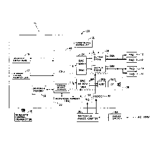
currents corresponding to a plurality of voltage waveforms at
different frequencies to an affected part has also been known. In
this case, for each of the voltage waveforms, the same waveform
is repeatedly used to apply a current for a given length of time.
[0004]
In such a conventional frequency therapy device, for each
frequency, a voltage waveform is formed each time, or waveform data
stored in a waveform memory is read, the data is converted to an
1
CA 03054634 2019-08-26
ZPF174PCICA
analog waveform by a D/A converter, and a predetermined waveform
is outputted.
[0005]
In this case, the voltage waveform or the waveform data is
a digital waveform generated by pulse width modulation (PWM) . As
compared to a case where an analog waveform is used as it is,
spike-shaped part in a rise portion and a fall portion in the digital
waveform depend on the number of quantization bits and the sampling
frequency thereof . However, in a shorter wavelength, in particular,
such spike-shaped part disappear.
[0006]
Since spike part have been conventionally regarded as noise,
no problem arises in that respect. In recent years, however, it
has been increasingly recognized that a higher voltage in a frequency
therapy device gives a greater impact on the human body and a greater
impact results in a larger effect of pain relief, for example.
[0007]
It can be readily envisaged that such a spike part can be formed
with a square wave having a narrow width. According to a result
(not publicly known) , however, when there are only spike part without
the presence of a subsequent high-level part or low-level part,
one feels that the pain relief effect is small (this fact has not
been known) . This can be considered that voltages (absolute values)
in the part (the high-level part and the low-level part) following
the spike part, an impact given by a top peak part or bottom peak
2
CA 03054634 2019-08-26
ZPF174PCTCA
part of such a spike part deforms diseased cells, for example, and
the high-level part and the low-level part keep the deformed state.
[0008]
In the case of using a digital waveform, on the other hand,
if a voltage is increased during use in a region of 2000 Hz or lower,
especially in a low-frequency region of 1000 Hz or lower, exceeding
about Level 3 causes electrified feeling even when the voltage can
be varied on a scale of 10 levels (from Level 1 to Level 10) , for
example. Thus, a shock or pain may be given to the human body.
[0009]
In this case, the frequency therapy device needs to be used
without exceeding Level 1 or 2, or Level 3 for some individuals.
Thus, voltages in the spike parts correspond to 1/3 or less of those
obtained when the level is raised to Level 10. This makes the user
feel that the pain relief effect is small. Similarly, it can be
considered that there is an appropriate range also for a pulse width
of the sharp-pointed top peak part.
[0010]
Furthermore, after therapy for a single code number (which
will be described later) is ended, a patient himself or herself,
or his or her assistance needs to perform an operation of newly
setting the next code number at the site of therapy. Thus, the process
is complicated, and a blank time is inadvantageously created before
setting the next code number.
Citation List
3
CA 03054634 2019-08-26
ZPF174PCTCA
Patent Literature
[0011] Patent Literature 1: U.S. Patent No. 5658322
Summary of Invention
Technical Problem
[0012]
An object of the present invention is to provide a frequency
therapy device capable of recording with a digital waveform so that
steep spike-shaped waveforms during a rise and a fall can be reliably
regenerated in a waveform memory referred to as a so-called sound
source chip, and capable of maintaining an impact given to a living
body by a sharp-pointed top peak part or a sharp-pointed bottom
peak part while reducing voltages (absolute values) in a high-level
part following the spike-shaped sharp-pointed top peak part and
a low-level part following the sharp-pointed bottom peak part, and
capable of passing a current while giving very little pain to the
patient's skin even in a low-frequency region.
[0013]
Another object of the present invention is to provide a
frequency therapy device having a low power consumption and suitable
for use as a portable frequency therapy device.
[0014]
A further object of the present invention is to provide a
frequency therapy device having no need to set a code number for
each therapy and thus placing less burden on a patient.
[0015]
4
The present invention provides a frequency therapy device
comprising: at least a pair of electrode pads capable of being in
contact with a human body with an affected part being interposed
therebetween; a main device unit that passes, between the pair of
electrode pads, a current corresponding to a voltage waveform in
which a direction thereof is reversed at regularly repeated time
intervals and a voltage increases and decreases alternately on a
positive side and a negative side; a display unit connected to the
main device unit for displaying a magnitude of a voltage applied
between the pair of electrode pads; and an operation/display panel
for operating the main device unit, wherein the main device unit
includes: a waveform memory that stores a plurality of voltage
waveforms at different frequencies; and a central control unit
configured to selectively read the plurality of voltage waveforms
stored in the waveform memory, and repeatedly and successively use
the read voltage waveform to pass a current between the pair of
electrode pads, the waveform memory stores the voltage waveform,
for each of the plurality of frequencies, as waveform data comprising
a square wave with a sampling frequency of 192 kHz or higher and
a number of quantization bits of 24 bits or more, and the central
control unit is configured to read the waveform data from the waveform
memory for each frequency, convert the waveform data to an analog
waveform by a D/A converter during a preset time for the frequency,
and pass a current corresponding to the voltage waveform between
the pair of electrode pads, the wavefoiln data stored in the waveform
5
Date Recue/Date Received 2021-04-28
memory has, within a single waveform period, a waveform ranging
from a rise part heading toward a positive region during a rise
transition period, through a sharp-pointed top peak part having
an overshoot shape at an end of the rise, a high-level part having
a smaller value than that of the sharp-pointed top peak part, a
fall part heading toward a negative region during a fall transition
period, a sharp-pointed bottom peak part having an undershoot shape
at an end of the fall, and a low-level part having a larger value
than that of the sharp-pointed bottom peak part, to a next rise
part, in a frequency range of at least 1000 Hz or lower, the waveform
data stored in the waveform memory has, within a single waveform
period, a waveform ranging from a rise part heading toward a positive
region from a O-V level during a rise transition period, through
a sharp-pointed top peak part having a spike shape at an end of
the rise and having a pulse width of 30 sec to 200 [isec, a high-level
part in which the voltage is larger than 0 V and smaller than or
equal to 5 V, a fall part heading toward a negative region during
a fall transition period, a sharp-pointed bottom peak part having
a spike shape at an end of the fall and having a pulse width of
30 [isec to 200 [isec, and a low-level part in which the voltage is
smaller than 0 V and larger than or equal to -5 V, to a next rise
part.
5a
Date Recue/Date Received 2021-04-28
, CA 03054634 2019-08-26
ZPF174PCTCA
[0016]
According to the present invention, spike part, i .e. , part
of a spike-shaped waveform, are referred to as the sharp-pointed
top peak part and the sharp-pointed bottom peak part. "Frequencies"
are defined to include low frequencies from 1 to 1000 Hz, medium
frequencies from 1000 to 10000 Hz, and high frequencies, which are
said to be 10000 Hz or higher but not clearly defined. The frequency
therapy device according to the present invention, however, involves
frequencies from 1 Hz to a high frequency of up to 30000 Hz, which
is considered to have influence on the human body. The numerical
values of a sampling frequency of 192 kHz and a number of quantization
bits of 24 bits come from the numerical values of an existing,
commercialized high-resolution uncompressed sound source. The
present invention also encompasses cases with sound source waveforms
having numerical values exceeding the aforementioned numerical
values.
Advantageous Effects of Invention
[0017]
The frequency therapy device according to the present invention
provides the advantageous effects that the spike part during the
rise and the spike part during the fall in the voltage waveform
to be appliedbetween the electrode pads can be accurately regenerated
at the same frequency and successively, and a shock on the human
body at portions where the electrode pads are attached can be reduced
and a power consumption can be significantly reduced by setting
6
CA 03054634 2019-08-26
ZPF174PCTCA
voltage values between the spike parts to a range of 0 to 5 V.
Brief Description of Drawings
[0018]
FIG. 1 is a block diagram showing a frequency therapy device
according to a first embodiment of the present invention.
FIG. 2 is a perspective view showing an external appearance
of the frequency therapy device.
FIG. 3 is a front view showing an operation/display panel of
the frequency therapy device.
FIG. 4 is a block diagram showing general configurations of
a central control unit and a waveform memory in the frequency therapy
device.
FIG. 5 is a chart showing an example of voltage waveforms stored
in the waveform memory.
FIG. 6 is a chart showing a relationship between a sampling
frequency and the number of quantization bits in a voltage waveform
stored in the waveform memory.
FIG. 7 is a flowchart showing a process of therapy performed
by the frequency therapy device.
FIG. 8 is a diagram showing examples of pad attachment positions
of the frequency therapy device.
FIG. 9 is a front view showing display examples of the operation
panel when a code is changed in the frequency therapy device.
FIG. 10 is a front view similarly showing display examples
of the operation panel when a code is newly registered.
7
CA 03054634 2019-08-26
ZPF174PCTCA
FIG. 11 is a front view similarly showing display examples
of the operation panel when a target code is deleted.
FIG. 12 is a front view similarly showing display examples
of the operation panel when all codes are deleted at once.
FIG. 13 is a plan view schematically showing a portable
frequency therapy device according to a second embodiment of the
present invention.
FIG. 14 is a front view showing an external appearance of the
frequency therapy device.
FIG. 15 is a block diagram showing general configurations of
a central control unit and a waveform memory in the frequency therapy
device.
FIG. 16 is a chart similar to FIG. 5, showing a state in which
voltage waveforms are stored in the waveform memory in a divided
manner for one minute each.
FIG. 17 is a chart showing a voltage waveform stored in a waveform
memory of a frequency therapy device according to a third embodiment
of the present invention.
Description of Embodiments
[0019]
Embodiments of the present invention will be described below
in detail with reference to the drawings.
First Embodiment
[0020]
As shown in FIG. 1 (a block diagram) and FIG. 2 (a perspective
8
CA 03054634 2019-08-26
ZPF174PCTCA
view showing an external appearance) , a frequency therapy device
according to a first embodiment of the present invention is
configured to include: two pairs of electrode pads 12, 12 and 14,
14, each pair being capable of being in contact with the human body
5 with an affected portion being interposed therebetween; a main device
unit 20 that passes, between the pair of electrode pads 12, 12 and/or
between the pair of electrode pads 14, 14 (hereinafter, referred
to as "between the electrode pads 12" for short) , a current
corresponding to a voltage waveform in which the direction thereof
10 is reversed at regularly repeated time intervals and a voltage
increases and decreases alternately on a positive side and a negative
side; an operation/display panel 16 connected to the main device
unit 20 for operating the main device unit 20 and providing various
kinds of display; an IR remote control reception unit 17 that performs
infrared transmission and reception, for example; an IR remote
control transmitter 18 for transmitting an operation signal to the
IR remote control reception unit 17; and a switching power adapter
28 for rectifying a 100 VAC input, which is inputted via a power
switch 16A included in the operation/display panel 16, and outputting
the rectified current to the main device unit 20.
[0021]
As shown in FIG. 3 in detail, the operation/display panel 16
includes: the power switch 16A; a group 16B of setting switches;
a code information display unit 160; a remaining therapy time display
unit 16D that displays, before therapy andduring a setting operation,
9
CA 03054634 2019-08-26
ZPF174PCTCA
a total time of set code numbers and displays, during therapy, a
remaining time of the therapy in a blinking manner; a current display
unit 16E that displays a current level during therapy; a START/PAUSE
switch 16F for starting/pausing/resuming therapy; an output increase
or decrease switch 16G for increasing or decreasing an output level
during therapy; an output display unit 16H that displays 32 levels
from 0 to 31 (0 = OFF) by means of bar representation, for example;
and an LED 161 for indicating that an output power (OUT) is on,
which has a yellow color, for example.
[0022]
The group 16B of setting switches includes: a SET switch 16B1
for setting a set value; an output channel (CH) selection switch
16B2 for selecting an output CH; a code setting dial 16B3 for setting
a code value; a RECORD switch 16B4 for storing a setting; and a
CLEAR switch 16B5 that, when being held down for three seconds or
more, for example, deletes all of set codes before therapy and deletes
the current code during a change.
[0023]
The code information display unit 160 includes: a number
up-down switch 1601 for selecting a code number; a code number display
unit 1602 that displays, before therapy, code numbers from 1 to
11, for example, which have been selected by the number up-down
switch 1601, and displays, during therapy, a code number of the
current therapy; an output CH display unit 1603 that displays, before
therapy, a CH setting for a number selected by the number up-down
. CA 03054634 2019-08-26
ZPF174PCTCA
switch 16C1, displays, during a change, an output CH selected by
the output channel selection switch 16B2 (the both are lit in the
case of the CH 1 and the CH 2 at the same time, and the CH 1 and
the CH 2 are both unlit in the case of an unregistered code "_ _
_ ") , and displays, during therapy, the selected CH of the current
_
code number; a code value display unit 16C4 that displays the code
value of a number selected by the number up-down switch 16C1; and
a code time display unit 16C5 that displays, before therapy, a code
time registered for each number by the number up-down switch 16C1
in minutes, for example, displays, during a code change, a time
registered in a code set by the code setting dial 16B3, and displays,
during therapy, a remaining time of the code of the current therapy,
for example, in a blinking manner.
[0024]
Alternatively, the entire operation/display panel 16 may be
configured as a single liquid crystal touch panel, for example.
[0025]
As shown in FIG. 1, the main device unit 20 includes: a waveform
memory 22 that stores a plurality of voltage waveforms at different
frequencies; and a central control unit (hereinafter, referred to
as a CPU) 40 that is configured to sequentially read the plurality
of voltage waveforms stored in the waveform memory 22 and pass a
current corresponding to the read voltage waveform between the pair
of electrode pads 12, 12.
[0026]
11
CA 03054634 2019-08-26
ZPF174PCTCA
The waveform memory 22 is what is called a sound source memory,
and stores a voltage waveform, for each of a plurality of frequencies,
as waveform data formed with a sampling frequency of 192 kHz or
higher and a number of quantization bits of 24 bits or more (which
will be described later in detail) .
[0027]
The CPU 40 is configured to read waveform data from the waveform
memory 22 for each frequency, output the waveform data to a D/A
converter 24 so as to be converted to an analog waveform during
a preset time for the frequency, and pass a current corresponding
to the voltage waveform between the electrode pads 12, 12.
[0028]
In addition to the waveform memory 22 and the D/A converter
24 described above, the main device unit 20 includes: an output
drive set 26 including a pair of output drives 26A and 26B; a DC/DC
converter 30; a regulator 32; a notification sound output system
36; and a minus voltage control unit 38.
[0029]
The D/A converter 24 is configured to perform a digital-analog
conversion on the waveform data read from the waveform memory 22
by the CPU 40 with a sampling frequency of 192 kHz or higher and
a number of quantization bits of 24 bits or more and output the
waveform data to the output drives 26A and 26B in an analog waveform.
[0030]
The output drives 26A and 26B are configured to change the
12
CA 03054634 2019-08-26
ZPF174PCTCA
outputs from the D/A converter 24 on the basis of the aforementioned
analog waveform and output the changed data to the electrode pads
12, 12 and the electrode pads 14, 14, respectively.
[0031]
The CPU 40 is configured to be able to output, to the output
drives 26A and 26B, a command signal to enable a mode in which the
output drives 26A and 26B are activated simultaneously, a mode in
which after the activation of one of the output drives 26A and 26B
is ended, the other one of the output drives 26A and 26B is successively
activated, or a mode in which the other one of the output drives
26A and 26B is continuously activated by repeating for a set number
of times under the same code in accordance with the setting of the
output CH selection switch 16B2 of the operation/display panel 16.
[0032]
The DC/DC converter 30 is configured to step down a
direct-current output from the switching power adapter 28 to a
predetermined voltage, and the regulator 32 is configured to turn
off the direct-current output when the output voltage and current
from the switching power adapter 28 unusually increase.
[0033]
A program memory 34 stores therein a program for operating
the CPU 40. The notification sound output system 36 plays, for
example, start-up sound when the power is turned on, therapy starting
sound at the start of therapy, therapy ending sound at the end of
therapy, error sound at the occurrence of an error (overcurrent,
13
CA 03054634 2019-08-26
ZPF174PCTCA
when started without the registration of a code, and the like),
output level operation sound at the time of operating an output
level, and the like. Specifically, the notification sound output
system 36 is configured to provide information to be notified, such
as "Ended" or "Will be paused," from a loudspeaker 36C by voice
when a condition to be notified to a patient occurs, including the
end of therapy.
[0034]
Such voice information is set in an extra storage region 22-A
( see FIG . 4) in the waveformmemory 22 . When a condition to be notified
occurs, the voice information is sent from the waveform memory 22
to a D/A converter 36A in the notification sound output system 36
on the basis of an instruction signal from the CPU 40, converted
to an analog signal in the D/A converter 36A, amplified by an amplifier
36B, and outputted as voice from the loudspeaker 36C.
[0035]
As will be described later, the minus voltage control unit
38 displaces the 0-V level in a voltage waveform toward the plus
side by 5% to 10% of the maximum voltage from the intermediate position
in the waveform chart so that an amount of electrons entering the
human body through the electrode pads 12, 12 becomes greater than
an amount of electrons escaping from the body. In this manner, the
minus voltage control unit 38 prevents the effects of deficiency
in electrons on the human body. Here, the reason for being set to
5% or more is because deficiency in electrons in the human body
14
CA 03054634 2019-08-26
ZPF174PCTCA
can be prevented from occurring even when a source voltage fluctuates.
The reason for being set to 10% or less is to prevent surplus in
electrons.
[0036]
As shown in FIG. 2, the IR remote control transmitter 18 is
provided with a remote control START/PAUSE switch 18F, which is
similar to the START/PAUSE switch 16F, and a remote control output
increase or decrease switch 18G, which is similar to the output
increase or decrease switch 16G. The IR remote control transmitter
18 is provided for each output CH (in the case of two channels,
two IR remote control transmitters 18 are provided in total). Note
that the remote control is not limited to an infrared remote control.
[0037]
The reference numerals 12A and 14A in FIG. 2 denote jacks for
receiving plugs 12B and 143 of the electrode pads 12 and 14. The
jacks 12A and 14A constitute a first output channel and a second
output channel, respectively.
[0038]
A configuration of the CPU 40 and the waveform memory 22 will
be described next.
[0039]
As shown in FIG. 4, the CPU 40 is configured to include: a
display signal outputting means 41; an operation switch signal
accepting means 42; an output channel selection signal accepting
means 43; a frequency set selection code signal accepting means
,
CA 03054634 2019-08-26
ZPF174POTCA
44; an operation signal accepting means 45; a frequency set selection
code output order and output mode (one of the pair, alternately,
or simultaneously) selection setting accepting means 46; a code
display signal outputting means 47; a code group voltage waveform
reading means 48; a voltage waveform outputting means 49; a DC/DC
converter driving means 50; a power ON/OFF means 51; a minus voltage
control means 52; an operation switch signal storing means 53; an
operation signal storing means 54; an output channel selection signal
storing means 55; a read voltage waveform storing means 56; a
code-associated frequency and order storing means 57; a frequency
set selection code signal storing means 58; a frequency set selection
code output order and output mode (one of the pair, alternately,
or simultaneously) selection setting storing means 59; and a
currently-outputted frequency storing means 60.
[0040]
The display signal outputtingmeans 41 is configuredto display,
at the output display unit 16H and the code number display unit
1602, output intensity and a code number operated by the output
increase or decrease switch 16G and the number up-down switch 1601
in the operation/display panel 16. The output channel selection
switch 16B2 itself is made as a touch panel. Each touch alternately
displays a number from "1" to "2" and from "2" to "1."
[0041]
The operation switch signal accepting means 42 is configured
to accept operation signals from the group 16B of setting switches
16
,
CA 03054634 2019-08-26
ZPF174PCTCA
in the operation/display panel 16. Moreover, the accepted signals
are stored in the operation switch signal storing means 53.
[0042]
The operation signal accepting means 45 is configured to accept
operation signals transmitted from the operation/display panel 16
and the IR remote control transmitter 18. The accepted operation
signals, specifically, an output intensity signal and a code number
signal to be described later, are stored in the operation signal
storing means 54.
[0043]
The output channel selection signal accepting means 43 is
configured to accept an output channel selection signal determined
by an operation of the output CH selection switch 16B2, and this
signal is stored in the output channel selection signal storing
means 55.
[0044]
The code display signal outputting means 47 is configured to
display information of an inputted code number at the code information
display unit 160 on the basis of a display signal stored in the
operation switch signal storing means 53.
[0045]
The code-associated frequency and order storingmeans 57 stores,
corresponding to a code, a plurality of frequencies predefined,
for each code, to be included in the code and their output order.
As shown in Table 1, for example, a frequency set selection code
17
CA 03054634 2019-08-26
ZPF174PCTCA
and the first to the n-th frequencies (n is a natural number greater
than or equal to two) are stored in combination. Specifically, for
the code number 1231, 20 Hz, 880 Hz, 5 kHz, ..., 10 kHz are stored
in this order.
[0046]
[Table 1]
NUMBER rUMENCY Maw), IMBENcy 11112E2122111
1231 20Hz 880Hz 5kHz 1 10kHz
1232 60Hz 125Hz 2128Hz 1111 5kHz
1467 72Hz 660Hz 2000Hz 10kHz
=
=
[0047]
The frequency set selection code output order and output mode
selection setting accepting means 46 is configured to accept
selection settings for frequency set selection code output order
and output mode (one of the pair, alternately, or simultaneously)
by the set order of the code setting dial 16B3 and an operation
of the output CH selection switch 16B2, and this signal is stored
in the frequency set selection code output order and output mode
selection setting storing means 59.
[0048]
On the basis of an inputted code signal and information stored
in the code-associated frequency and order storing means 57 and
18
CA 03054634 2019-08-26
ZPF174PCTCA
the frequency set selection code output order and output mode
selection setting storing means 59, the code group voltage waveform
readingmeans 48 is configured to sequentially read, from the waveform
memory 22, the voltage waveforms at the plurality of frequencies
included in the code in accordance with the output order and the
output mode (one of the pair, alternately, or simultaneously) stored
in the read voltage waveform storing means 56.
[0049]
The voltage waveform outputting means 49 is configured to
output, to the D/A converter 24, data on the voltage waveforms at
the frequencies read by the code group voltage waveform reading
means 48.
[0050]
The DC/DC converter driving means 50 is configured to drive
the DC/DC converter 30 in accordance with the output intensity
operated by the output increase or decrease switch 16G.
[0051]
The power ON/OFF means 51 is configured to turn on or off a
100 VAC input to the switching power adapter 28 in accordance with
an operation of the power switch 16A.
[0052]
The currently-outputted frequency storing means 60 is
configured to store the frequency of the waveform data being currently
outputted from the voltage waveform outputting means 49.
[0053]
19
CA 03054634 2019-08-26
ZPF174PCTCA
The operation switch signal accepting means 42 is configured
to turn off the DC/DC converter 30 by the regulator 32 so as to
interrupt current supply from the output drive set 26 when an
interruption signal for interrupting therapy is inputted by an
operation of the remote control START/PAUSE switch 18F in the IR
remote control transmitter 18 during therapy provided by the
frequency therapy device 10.
[0054]
The code group voltage waveform reading means 48 in this case
is configured to read frequency information at the time of the
interruption, which has been stored in the currently-outputted
frequency storing means 60, and read the voltage waveform at that
frequency when the therapy is resumed.
[0055]
The waveform memory 22 includes N (Nis a natural number greater
than or equal to two) waveform storage regions 22-1 to 22-N, and
the number of therapy frequencies used in the frequency therapy
device 10 in this embodiment is N. Voltage waveforms at the N
frequencies are stored in any of the waveform storage regions 22-1
to 22-N for each frequency.
[0056]
FIG. 5 shows an example of recorded states of voltage waveforms
in the waveform storage regions of the waveform memory 22. FIG.
5 schematically shows the states of the voltage waveforms, in the
case of the code number 1231, for example, at four frequencies of
CA 03054634 2019-08-26
ZPF174PCTCA
20 Hz, 880 Hz, 5 kHz, and 10 kHz belonging to this code number.
[0057]
In each of the waveform storage regions 22-1 to 22-N in the
waveform memory 22, a voltage waveform at the same frequency and
having the same waveform is successively and repeatedly stored for
three minutes. In the case of a frequency of 20 Hz, for example,
the same voltage waveform is repeatedly stored to have 3 (minutes)
x 60 (seconds) x 20 = 3600 voltage waveforms in total. A distance
between the voltage waveforms is constant, and there is no overlapping
or separation between adjacent ones of the waveforms.
[0058]
Each voltage waveform is basically in a state as shown in FIG.
6, has a number of quantization bits of 24 bits or more and a sampling
frequency of 192 kHz, and is formed by a digital signal divided
into a time corresponding to the inverse of the sampling frequency.
In the case of a frequency of 20 Hz, for example, a waveform for
1/20 second (the inverse of the frequency) is constituted of 192
kHz/20 Hz =9600 pulses.
[0059]
A voltage in a high-level part HL and a voltage in a low-level
part LL have a maximum value of +5 V and a minimum value of -5 V,
respectively.
[0060]
As shown in FIG. 6 in an enlarged manner, waveform data stored
in each of the waveform storage regions in the waveform memory 22
21
CA 03054634 2019-08-26
ZPF174PCTCA
has, within a single waveform period, a waveform Df ranging from
a rise part Up heading toward a positive region during a rise
transition period, through a sharp-pointed top peak part Tp having
a spike shape at the end of the rise, the high-level part HL having
a smaller value than that of the sharp-pointed top peak part Tp,
a fall part Dw heading toward a negative region during a fall
transition period, a sharp-pointed bottom peak part Bp having a
spike shape at the end of the fall, and the low-level part LL having
a larger value than that of the sharp-pointed bottom peak part Bp,
to the next rise part Up.
[0061]
A height (absolute value) between tips of the sharp-pointed
top peak part Tp and the sharp-pointed bottom peak part Bp represents
the maximum voltage, and each of a voltage at the sharp-pointed
top peak part Tp and a voltage at the sharp-pointed bottom peak
part Bp can be expressed by the maximum value corresponding to a
number of quantization bits of 24 bits on a plus side or a minus
side. In the waveform shown in FIG. 6, the sharp-pointed top peak
part Tp and the sharp-pointed bottom peak part Bp corresponded to
35 V and -35 V, respectively, and the maximum voltage was 1+351
+ 1-351 = 70 V. Each of the maximum pulse widths Wtp and Wbp of the
sharp-pointed top peak part Tp and the sharp-pointed bottom peak
part Bp was about 110 sec.
[0062]
Here, the pulse widths Wtp and Wbp of the sharp-pointed top
22
CA 03054634 2019-08-26
ZPF174PCTCA
peak part Tp and the sharp-pointed bottom peak part Bp in the
above-described waveform Df are defined to be 30 sec to 200 sec
in a frequency range of 1000 Hz or lower. The reason for being set
to 30 sec or more is because a pulse width smaller than 30 sec
results in a very small pain relief effect or gives a patient no
sense of undergoing therapy, for example.
[0063]
For a maximum width of 300 sec, for example, an impact given
to a patient became strong, thereby causing a sense of discomfort.
[0064]
In terms of a relationship with a frequency, a wavelength time
for one waveform is 0.001 sec = 1000 sec in the case of 1000 Hz,
for example. Of 1000 sec, 300 sec x 2 = 600 sec corresponds to
the pulse widths Wtp and Wbp of the sharp-pointed top peak part Tp
and the sharp-pointed bottom peak part Bp. Thus, a pulse width of
the part of 0 to 5 V between the sharp-pointed top peak part Tp
and the sharp-pointed bottom peak part Bp becomes smaller than the
sharp-pointed top peak part Tp and the sharp-pointed bottom peak
part Bp. This reduces the effect of reducing power consumption and
also reduces the effect of giving an accurate impact on an affected
part by the sharp-pointed top peak part Tp and the sharp-pointed
bottom peak part Bp.
[0065]
When each of the pulse widths Wtp and Wbp of the sharp-pointed
top peak part Tp and the sharp-pointed bottom peak part Bp is set
23
CA 03054634 2019-08-26
ZPF174PCTCA
to 60 sec or less, the above-described effect of reducing power
consumption can be obtained over 1000 Hz and even up to 2000 Hz.
[0066]
Moreover, the CPU 40 is configured so that two different
frequency set selection codes can be inputted via the frequency
set selection code signal accepting means 44 by switching the output
CH selection switch 16B2 in the operation/display panel 16, and
such a frequency set selection code is stored in the frequency set
selection code signal storing means 58. Pieces of waveform data
for a plurality of frequencies preset corresponding to an inputted
frequency set selection code are sequentially read from the waveform
storage regions 22-1 to 22-N of the waveform memory 22 that store
the pieces of waveform data in a predefined order during a set time
for each frequency, and then outputted.
[0067]
Furthermore, the CPU 40 is configured to include the
code-associated frequency and order storing means 57 that stores
a frequency set selection code, frequencies corresponding to this
frequency set selection code, and an output order of pieces of waveform
data for these frequencies; the code group voltage waveform reading
means 48 that reads, from the waveform memory 22, the pieces of
waveform data for the frequencies in accordance with the order stored
in the code-associated frequency and order storing means 57 and
the frequency set selection code output order and output mode
selection setting storing means 59; and the voltage waveform
24
CA 03054634 2019-08-26
ZPF174PCTCA
outputting means 49 that outputs the pieces of waveform data read
by the code group voltage waveform reading means 48 in the
aforementioned order.
[0068]
Two output drive sets 26 are provided in the first embodiment.
The CPU 40 is configured so that an output channel can be selected
by the output CH selection switch 16B2; for each of the first and
second output channels, a code different for each of the selected
11 code numbers from "01" to "11" can be set by the number up-down
switch 16C1; and a direct current can be first supplied only to
the output drive 26A, of the two output drives 26A and 26B, and
a direct current can be supplied to the other output drive 26B only
after the completion of the supply of the direct current by the
output drive 26A, for example. Alternatively, an output can be
provided alternately from the first output channel and the second
output channel, outputs can be provided simultaneously to treat
two persons, or two outputs outputted to a person can be caused
to interfere with each other.
[0069]
In the first embodiment, the output drive 26A of the first
channel and the output drive 26B of the second channel are independent
of each other to constitute fully parallel two channels. Thus, as
compared to a case where a single channel is simply split into two
channels, an increased amount of current flowing through one of
the channels causes no reduced amount of current flowing through
CA 03054634 2019-08-26
ZPF174PCTCA
the other one of the channels. Moreover, currents corresponding
to different codes can be caused to flow through the two channels.
[0070]
With reference to FIG. 7, a process of therapy performed by
the frequency therapy device 10 of the above-described embodiment
will be described next.
[0071]
In step S100, the electrode pads 12 (or 14) are first attached
to predetermined sites depending on a pain relief target as shown
in FIG. 8 as an example. FIG. 8A shows an example in which the pair
of electrode pads 12 are attached to the target right flank, and
FIG. 8B shows an example in which the pair of electrode pads 14
are attached to the target right and left flanks. Note that the
positions of the electrode pads 12 and 14 are not limited to the
above positions, but may be the soles of the feet, for example.
[0072]
To start therapy, the power switch 16A is first turned on in
step S101 to power up the device. After the respective parts are
all lit by lighting all LEDs once, pieces of code information (a
code, a time, an output CH, and a therapy time) are displayed. The
pieces of code information are the same as the previous settings
before the power is turned off. At the same time, start-up sound
is emitted.
[0073]
Next, in step S102, the operation/display panel 16 is turned
26
CA 03054634 2019-08-26
ZPF174PCTCA
on to obtain a state in which a therapy code can be set by the group
16B of setting switches.
[0074]
In step S103, the output drives 26A and 26B are sequentially
selected and an output mode is selected by operations of the output
channel selection switch 1 6B2 . Thereafter, for each of the selected
codes, a four-digit therapy code is set by the code setting dial
16B3 while viewing the code value display unit 1604 (a therapy code
may be set only for the output drive 26A).
[0075]
In the following step S104, the setting is registered by the
RECORD switch 16B4, and the change is ended. This activates the
code group voltage waveform reading means 48, thereby obtaining
a state in which data on a waveform for each frequency can be
sequentially read, as a voltage waveform at the first, second, ...,
or n-th frequency, on the basis of a signal from the code-associated
frequency and order storing means 57, from any of the waveform storage
regions 22-1 to 22-N in the waveform memory 22 in accordance with
the stored order.
[0076]
A case where the set code is changed is shown in FIG. 9 as
an example. The eleven code numbers from 01 to 11 can be set.
[0077]
First, as shown in FIG. 9A, the current code information (in
the figure, a code number of 01, an output CH of 2, a code value
27
,
,
CA 03054634 2019-08-26
ZPF174PCTCA
of 0005, and a time of 036 minutes used in the previous therapy,
for example) is still shown and this information is checked. If
there is no need to change the information, setting for the next
code number 02 is started.
[0078]
First, the code number is changed by the number up-down switch
16C1. In FIG. 9B, while the code number is changed from 01 to 02,
an output CH of CH 2, a code value of 0021, and a time of 027 used
in the previous therapy are still shown.
[0079]
Next, as shown in FIG. 90, pressing the SET switch 16B1 causes
the LEDs of NO, CODE, and TIME, and the output CH display unit 1603
to blink, and a state in which a change can be made is obtained.
At this time, the code value is changed by turning the code setting
dial 16B3.
[0080]
Next, the output CH is changed (the CH 1 or the CH 2, or the
CH 1 and the CH 2 at the same time) by the output CH selection switch
16B2 as shown in FIG. 9D. FIG. 9D shows an example in which the
code value has been changed to "0005" and the output CH has been
set to the CH 1 and the CH 2 at the same time. Since a time and
a code value are defined as a set, "036" corresponding to "0005"
is displayed.
[0081]
Next, as shown in FIG. 9E, the RECORD switch 16B4 is pressed
28
CA 03054634 2019-08-26
ZPF174PCTCA
to register the settings. This changes the blinking state to a lit
state, and ends the change.
[0082]
Next, a case where a code number of 03 is selected and an
unregistered code that has not been previously used is set will
be shown in FIG. 10.
[0083]
First, an unregistered number is displayed as " _ " as
_ _
shown in FIG. 10A. At this time, pressing the SET switch 1681 results
in a state in which a change can be made. Registration is performed
by the same operations as those at the time of the aforementioned
change.
[0084]
More specifically, the code value is changedby the code setting
dial 1683, and the CH output is changed (the CH 1 or the CH 2, or
the CH 1 and the CH 2 at the same time) by the output CH selection
switch 1682 as shown in FIG. 10B.
[0085]
FIG. 100 shows an example in which the code value "0017" has
been registered, and the output CH has been set to the CH1 and the
CH2 at the same time.
[0086]
Next, as shown in FIG. 10D, the RECORD switch 1684 is pressed
to register the settings. This changes the blinking state to the
lit state, and ends the registration.
29
CA 03054634 2019-08-26
ZPF174PCTCA
[0087]
A case where the registration of a single target code is deleted
is shown in FIG. 11.
[0088]
In this case, a code number (e.g.,"03") the user wishes to
delete is selected by the number up-down switch 16C1, and then the
SET switch 16B1 is pressed to obtain a state in which a change can
be made as shown in FIG. 11A.
[0089]
Next, in the state in which a change can be made (blinking),
the CLEAR switch 16B5 is held down for three seconds, for example,
to cancel the registration as shown in FIG. 11B.
[0090]
Next, the RECORD switch 16B4 is pressed to register the setting
and the deletion is ended as shown in FIG. 11C.
[0091]
The end state is shown in FIG. 11D. A new code can be immediately
inputted by the code setting dial 16B3.
[0092]
A case where the registration of all codes is deleted at once,
as in a case where codes are newly inputted from scratch, is shown
in FIG. 12.
[0093]
In this case, the CLEAR switch 16B5 is held down for three
seconds, for example, to cancel the registrations as shown in FIG.
-
CA 03054634 2019-08-26
ZPF174PCTCA
12A.
[0094]
This cancels all of the registered codes as shown in FIG. 12B.
[0095]
After the end of step S104 in FIG. 7, the START/PAUSE switch
16F is turned on in the following step S105. In the following step
S106, the voltage waveform at the first frequency is selected, and
the voltage waveform stored, for example, in the waveform storage
region 22-2 of the waveform memory 22 is read. Since the voltage
waveform for three minutes is successively stored in the waveform
storage region 22-2, an analog output corresponding to the voltage
waveform at the first frequency is generated from the output drive
26A in step S107.
[0096]
Here, when the present output mode stored in the frequency
set selection code output order and output mode selection setting
storing means 59 is the output channel 2, the analog output is
generated from the output drive 26B. When the alternate output mode
is stored, the output is generated alternately from the output drives
26A and 26B. When the simultaneous output mode is stored, outputs
are generated fromboth of the output drives 2 6A and 2 6B simultaneously.
When the outputs are generated simultaneously, the outputs can be
provided to two persons simultaneously, or the two outputs can be
applied to a person simultaneously and the two outputs can be caused
to interfere with each other by crossing, for example.
31
CA 03054634 2019-08-26
ZPF174PCTCA
[0097]
Immediately after a pulse is generated, output intensity
indicated in the output display unit 16H of the operation/display
panel 16 is adjusted in the following step S108 by an operation
of the output increase or decrease switch 16G also included in the
operation/display panel 16 to a level at which no pain is caused
at the portions of the electrode pads that are in contact with the
patient, for example.
[0098]
The analog output corresponding to the voltage waveform at
the first frequency continues for three minutes. To interrupt the
therapy halfway due to some problem, however, the remote control
START/PAUSE switch 18F is activated by the IR remote control
transmitter 18, and such activation serves as an interruption switch .
In step S109, "Yes" is selected, and the analog output returns to
zero at step S111. At the same time, notification sound such as
"Will be paused" is outputted from the loudspeaker 36C.
[0099]
If no interruption switch is turned on during these three
minutes, "No" is selected in step S109, and the process proceeds
to step 5110. After three minutes of the analog output generation
time, the output returns to zero.
[0100]
If the remote control START/PAUSE switch 18F is activated by
the IR remote control transmitter 18 after the output is returned
32
CA 03054634 2019-08-26
ZPF174PCTCA
to zero by turning the interruption switch on, on the other hand,
such activation serves to turn a restart switch on. In step 5112,
"Yes" is selected, and the process returns to step S107. If "No,"
the process returns to step S112.
[0101]
After the end of step S110, the next voltage waveform at the
second frequency is selected in the following step S113. In the
following step S114, an analog output corresponding to the voltage
waveform at the second frequency selected in step S113 is generated.
[0102]
As with the case of the voltage waveform at the first frequency,
output intensity is adjusted in step S115, and whether the
interruption switch is turned on is determined in step S116. If
"Yes," the process proceeds to step S117. After steps S111 and S112
are repeated, the process returns to step S113.
[0103]
If the determination on whether the interruption switch is
turned on is "No" in step S116, then the process proceeds to step
S118 where the output returns to zero after three minutes of the
generation of the analog output corresponding to the voltage waveform
at the second frequency. In the following step S119, the
above-described steps from S106 through S112 are repeated for each
of the subsequent third to the n-th frequencies. After three minutes
of the generation of the analog output for the n-th frequency, the
process proceeds to step S120.
33
CA 03054634 2019-08-26
ZPF174PCTCA
[0104]
In step 5120, whether the next therapy code has been set and
stored in the frequency set selection code output order and output
mode selection setting storing means 59 is determined. If "No,"
then the process proceeds to step S124 and an ending lamp and a
buzzer are turned on. More specifically, the end of the therapy
is notifiedto thepatient fromthe loudspeaker 36Cof thenotification
sound output system 36. The patient or his or her assistance then
turns off the power switch 16A, thereby ending the process at step
S125.
[0105]
If the output of the next therapy code for the output drive
26B has been set and stored by the output CH selection switch 16B2,
the determination result at step S120 is "Yes." Whether pad
attachment positions need to be changed is determined in step S121.
If the determination result is "Yes," the process proceeds to step
S122 to change the pad attachment positions.
[0106]
After the end of step S122, or if the determination result
in step S121 is "No," then the process proceeds to step S123 to
repeat the above-described steps from S106 through S119 for the
next therapy code. After the end of those steps, the process returns
to step S120.
Second Embodiment
[0107]
34
CA 03054634 2019-08-26
ZPF174PCTCA
A second embodiment of the present invention for a portable
type will be described next in detail with reference to the drawings.
[0108]
As shown in FIG. 13 (a block diagram) and FIG. 14 (a front
view showing an external appearance), a frequency therapy device
70 according to the second embodiment of the present invention is
configured to include: a pair of electrode pads 72 capable of being
in contact with the human body with an affected part being interposed
therebetween; a main device unit 80 that passes, between the pair
of electrode pads 72, a current corresponding to a voltage waveform
in which the direction thereof is reversed at regularly repeated
time intervals and a voltage increases and decreases alternately
on a positive side and a negative side; a display unit 76A connected
to the main device unit 80 for displaying a magnitude of a voltage
appliedbetween the electrode pads 72 and a code; an operation/display
panel 76 including a panel operation switch unit 76B for operating
the main device unit 80; and a battery 90 incorporated in the main
device unit 80.
[0109]
The main device unit 80 includes: a waveform memory 82 that
stores a plurality of voltage waveforms at different frequencies;
and a central control unit (hereinafter, referred to as a CPU) 100
that is configured to sequentially read the plurality of voltage
waveforms stored in the waveform memory 82 and pass a current
corresponding to the read voltage waveform between the pair of
CA 03054634 2019-08-26
ZPF174PCTCA
electrode pads 72.
[0110]
The waveform memory 82 is what is called a sound source memory,
and stores a voltage waveform, for each of a plurality of frequencies,
as waveform data formed with a sampling frequency of 192 kHz or
higher and a number of quantization bits of 24 bits or more as mentioned
above.
[0111]
The CPU 100 is configured to read waveformdata from the waveform
memory 82 for each frequency, output the waveform data to a D/A
converter 84 so as to be converted to an analog waveform during
a preset time for the frequency, and pass a current corresponding
to the voltage waveform between the electrode pads 72.
[0112]
In addition to the waveform memory 82 and the D/A converter
84 described above, the main device unit 80 includes: an output
drive 86; an alarm 96; and a minus voltage control unit 98.
[0113]
The D/A converter 84 is configured to perform a digital-analog
conversion on the waveform data read from the waveform memory 82
by the CPU 100 with a sampling frequency of 192 kHz or higher and
a number of quantization bits of 24 bits or more and output the
waveform data to the output drive 86 in an analog waveform.
[0114]
The output drive 86 is configured to change an output from
36
CA 03054634 2019-08-26
ZPF174PCTCA
the battery 90 on the basis of the aforementioned analog waveform
and provide the changed output to the respective electrode pads
72.
[0115]
The CPU 100 controls the output drive 86 to provide an output
in accordance with a command signal from the panel operation switch
unit 763.
[0116]
A program memory 94 stores therein a program for operating
the CPU 100. The alarm 96 is configured to emit an alarm when a
condition to be notified to a patient occurs, including the end
of therapy.
[0117]
As mentioned above, the minus voltage control unit 98 displaces
the 0-V level in a voltage waveform toward the plus side by 5% to
10% of the maximum voltage from the intermediate position in the
waveform chart, so that an amount of electrons entering the human
body through the electrode pads 72 becomes greater than an amount
of electrons escaping from the body. In this manner, the minus
voltage control unit 98 prevents the effects of deficiency in
electrons on the human body. Here, the reason for being set to 5%
or more is because deficiency in electrons in the human body can
be prevented from occurring even when a source voltage fluctuates.
The reason for being set to 10% or less is to prevent surplus in
electrons.
37
CA 03054634 2019-08-26
ZPF174PCTCA
[0118]
As shown in FIG. 14, the display unit 76A of the
operation/display panel 76 is configured to include: a numerical
value display section 77A that displays a code number or a code
value, and a remaining time of therapy; and a graph display section
77B that displays an output.
[0119]
A power switch 77D, a START/PAUSE switch 77E for
starting/pausing/resuming therapy, and an up-down setting switch
77F for increasing or decreasing output intensity from the output
drive 86 and setting a code number or a code value are disposed
in the panel operation switch unit 76B.
[0120]
The reference numeral 72A in FIG . 14 denotes a j ack for receiving
a plug 72B of the electrode pads 72.
[0121]
A configuration of the CPU 100 and the waveform memory 82 will
be described next.
[0122]
As shown in FIG. 15, the CPU 100 is configured to include:
a display signal outputting means 101; an operation switch signal
accepting means 102; a frequency set selection code signal accepting
means 104; an operation signal accepting means 105; a code display
signal outputting means 107; a code group voltage waveform reading
means 108; a voltage waveform outputting means 109; a power ON/OFF
38
,
CA 03054634 2019-08-26
ZPF174PCTCA
means 111; a minus voltage control means 112; an operation switch
signal storing means 113; an operation signal storing means 114;
a read voltage waveform storing means 116; a code-associated
frequency and order storing means 117; a frequency set selection
code signal storing means 118; and a currently-outputted frequency
storing means 120.
[0123]
The display signal outputting means 101 is configured to
display, at the numerical value display section 77A and the graph
display section 77B in the display unit 76A, output intensity, and
a code number or a code value operated by the up-down setting switch
77F in the operation/display panel 76.
[0124]
The operation switch signal accepting means 102 is configured
to accept operation signals from the panel operation switch unit
76B of the operation/display panel 76. Moreover, the accepted
signals are stored in the operation switch signal storing means
113.
[0125]
The operation signal accepting means 105 is configured to
accept operation signals transmitted from the panel operation switch
unit 76B. The accepted operation signals, specifically, an output
intensity signal and the aforementioned code number signal, are
stored in the operation signal storing means 114.
[0126]
39
CA 03054634 2019-08-26
ZPF174PCTCA
The code display signal outputting means 107 is configured
to display an inputted code number at the display unit 76A on the
basis of a display signal stored in the operation switch signal
storing means 113.
[0127]
The code-associated frequency and order storing means 117
stores, corresponding to a code, a plurality of frequencies
predefined, for each code, to be included in the code and their
output order. As shown in the aforementioned Table 1, for example,
a frequency set selection code and the first to the n-th frequencies
(n is a natural number greater than or equal to two) are stored
in combination. Specifically, for the code number 1231, 20 Hz, 880
Hz, 5 kHz, ..., 10 kHz are stored in this order.
[0128]
On the basis of an inputted code signal and information stored
in the code-associated frequency and order storing means 117, the
code group voltage waveform reading means 108 is configured to
sequentially read, from the waveformmemory 82, the voltage waveforms
at the plurality of frequencies included in the code.
[0129]
The voltage waveform outputting means 109 is configured to
output, to the D/A converter 84, data on the voltage waveforms at
the frequencies read by the code group voltage waveform reading
means 108.
[0130]
,
,
CA 03054634 2019-08-26
ZPF174PCTCA
The power ON/OFF means 111 is configured to turn on or off
the output of the battery 90 to the output drive 86 in accordance
with an operation of the power switch 77D.
[0131]
The currently-outputted frequency storing means 120 is
configured to store the frequency of the waveform data being currently
outputted from the voltage waveform outputting means 109.
[0132]
The operation switch signal accepting means 102 is configured
to turn off the output of the battery 90 to the output drive 86
so as to interrupt current supply from the output drive 86 when
an interruption signal for interrupting therapy is inputted during
therapy provided by the frequency therapy device 70.
[0133]
The code group voltage waveform reading means 108 in this case
is configured to read frequency information at the time of the
interruption, which has been stored in the currently-outputted
frequency storing means 120, and read the voltage waveform at that
frequency when the therapy is resumed.
[0134]
The waveform memory 82 includes N (N is a natural number greater
than or equal to two) waveform storage regions 82-1 to 82-N, and
the number of therapy frequencies used in the frequency therapy
device 70 in this embodiment is N. Voltage waveforms at the N
frequencies are stored in any of the waveform storage regions 82-1
41
CA 03054634 2019-08-26
ZPF174PCTCA
to 82-N for each frequency.
[0135]
The other elements are the same as those of the first embodiment,
and thus the detailed description thereof will be omitted.
[0136]
While a voltage waveform is successively stored for three
minutes in each of the waveform storage regions 22-1 to 22-N in
the waveform memory 22 in the above-described first embodiment,
the present invention is not limited thereto. When the voltage
waveform storage capacity of the waveform memory 22 is insufficient,
for example, voltage waveforms may be stored only fora time obtained
by dividing a set time (three minutes in the embodiment) by two
or three, and the voltage waveforms may be read twice or three times
for a single duration of the set time. FIG. 16 shows a case where
three minutes are divided into three, and voltage waveforms are
read three times for one minute each.
[0137]
In the above-described embodiments, the sampling frequency
is 192 kHz and the number of quantization bits is 24 bits. This
is because what is called a sound source chip is used as the waveform
memory and the upper limit of the sound chip corresponds to 192
kHz and 24 bits. The present invention can be also applied to cases
exceeding 192 kHz and 24 bits.
[0138]
As shown in FIG. 6, in the voltage waveform (waveform data)
42
CA 03054634 2019-08-26
ZPF174PCTCA
stored in the waveform memory in the above-described first embodiment,
a voltage in the high-level part HL has a maximum value of +5 V
and a voltage in the low-level part LL has a minimum value of -5
V. These values are set to be significantly smaller than those of
the sharp-pointed top peak part Tp and the sharp-pointed bottom
peak part Bp. For a patient less likely to feel pain for current,
voltages (absolute values) in the high-level part HL and the low-level
part LL can be set larger than the above-described values as in
a voltage waveform of a third embodiment shown in FIG. 17, for example .
[0139]
In this case, a deformed state of diseased cells that is caused
by an impact given to the human body by the sharp-pointed top peak
part Tp and the sharp-pointed bottom peak part Bp can be more reliably
kept until the start of deformation due to an impact in the reverse
direction.
Industrial Applicability
[0140]
The present invention can be applied to the field of frequency
therapy devices such as low-frequency therapy devices.
Reference Signs List
[0141]
10, 70 ... frequency therapy device
12, 14, 72 ... electrode pad
12A ... jack (first output channel)
14A ... jack (second output channel)
43
CA 03054634 2019-08-26
ZPF174PCTCA
16, 76 operation/display panel
16A, 77D power switch
16B group of setting switches
16B1 SET switch
16B2 output channel (CH) selection switch
16B3 code setting dial
16B4 RECORD switch
16B5 CLEAR switch
16C code information display unit
16C1 number up-down switch
16C2 code number display unit
16C3 output CH display unit
16C4 code value display unit
16C5 code time display unit
16D remaining therapy time display unit
16E current display unit
16F, 77E START/PAUSE switch
16G output increase or decrease switch
16H output display unit
161 LED for indicating that output power is on
17 IR remote control reception unit
18 IR remote control transmitter
18F remote control START/PAUSE switch
18G remote control output increase or decrease switch
20, 80 main device unit
44
CA 03054634 2019-08-26
ZPF174PCTCA
22, 82 _ waveform memory
21-1 to 22-N, 82-1 to 82-N _ waveform storage region
22-A _ extra storage region
24, 84 _ D/A converter
26 _ output drive set
26A, 26B, 86 _ output drive
28 _ switching power adapter
30 _ DC/DC converter
32 _ regulator
34, 94 _ program memory
36 _ notification sound output system
36A, 84 _ D/A converter
36B _ amplifier
36C _ loudspeaker
38, 98 _ minus voltage control unit
40, 100 _ central control unit (CPU)
41, 101 _ display signal outputting means
42, 102 _ operation switch signal accepting means
43 _ output channel selection signal accepting means
44, 104_ frequency set selection code signal accepting means
45, 105 _ operation signal accepting means
46 _ frequency set selection code output order and output
mode selection setting accepting means
47, 107 _ code display signal outputting means
48, 108 _ code group voltage waveform reading means
CA 03054634 2019-08-26
ZPF174PCTCA
49, 109 voltage waveform outputting means
50 DC/DC converter driving means
51, 111 power ON/OFF means
52, 112 minus voltage control means
53, 113 operation switch signal storing means
54, 114 operation signal storing means
55 output channel selection signal storing means
56, 116 read voltage waveform storing means
57, 117 code-associated frequency and order storing means
58, 118 frequency set selection code signal storing means
59 frequency set selection code output order and output
mode selection setting storing means
60, 120 currently-outputted frequency storing means
76A display unit
76B panel operation switch unit
77A numerical value display section
77B graph display section
77F up-down setting switch
90 battery
96 alarm
98 minus voltage control unit
46