Note : Les descriptions sont présentées dans la langue officielle dans laquelle elles ont été soumises.
CA 03056787 2019-09-16
WO 2018/175542 PCT/US2018/023505
METHOD AND SYSTEM FOR FIBER SCANNING PROJECTOR
CROSS-REFERENCES TO RELATED APPLICATIONS
[0001.1 This application claims priority to U.S. Provisional Patent
Application No.
62/474,461, filed on March 21, 2017, entitled "Method and System for Fiber
Scanning
Projector," the disclosure of which is hereby incorporated by reference in its
entirety for all
purposes.
BACKGROUND OF THE INVENTION
100021 Modern computing and display technologies have facilitated the
development of
systems for so called "virtual reality" or "augmented reality" experiences,
wherein digitally
reproduced images or portions thereof are presented to a viewer in a manner
wherein they
seem to be, or may be perceived as, real. A virtual reality, or "VR," scenario
typically
involves presentation of digital or virtual image information without
transparency to other
actual real-world visual input; an augmented reality, or "AR," scenario
typically involves
presentation of digital or virtual image information as an augmentation to
visualization of the
actual world around the viewer.
100031 Despite the progress made in these display technologies, there is a
need in the art for
improved methods and systems related to augmented reality systems,
particularly, display
systems.
SUMMARY OF THE INVENTION
[0004] The present invention relates generally to methods and systems related
to projection
display systems including wearable displays. More particularly, embodiments of
the present
invention provide methods and systems for volumetric displays, also referred
to as a light
field displays, that create volumetric sculptures of light at more than one
depth plane. The
invention is applicable to a variety of applications in computer vision and
image display
systems.
=
CA 03056787 2019-09-16
=
WO 2018/175542 PCT/US2018/023505
[0005] According to an embodiment of the present invention, a projector is
provided. The
projector includes a scanning light source defining a convex object surface
and an optical
assembly section operable to receive light from the scanning light source. The
optical
assembly section includes a prism element; a collimating element coupled to
the prism
element at an interface; a quarter wave plate; and a polarizing beam splitter
disposed at the
interface.
[00061 According to an embodiment of the present invention, a fiber scanning
projector is
provided. The fiber scanning projector includes a piezoelectric element, a
scanning fiber
mechanically coupled to the piezoelectric element, and an optical assembly
section operable
to receive light from the scanning fiber. The optical assembly section
includes a prism
element, a collimating element coupled to the prism element at an interface, a
quarter wave
plate, and a polarizing beam splitter disposed at the interface.
[0007] According to another embodiment of the present invention, a fiber
scanning
projector is provided. The fiber scanning projector includes a piezoelectric
element and a
scanning fiber passing through and mechanically coupled to the piezoelectric
element. The
scanning fiber emits light along an optical path. The fiber Scanning projector
also includes a
mirror including an aperture. The scanning fiber passes through the aperture.
The fiber
scanning projector further includes a collimating mirror disposed along the
optical path.
100081 According to a specific embodiment of the present invention, a fiber
scanning
projector is provided. The fiber scanning projector includes a piezoelectric
element and a
scanning fiber passing through and mechanically coupled to the piezoelectric
element. The
scanning fiber emits light along an optical path. The fiber scanning projector
also includes a
first polarization sensitive reflector disposed along the optical path, a
quarter wave plate
disposed adjacent the first polarization sensitive reflector, and a second
polarization sensitive
reflector disposed along the optical path.
[0009] Numerous benefits are achieved by way of the present invention over
conventional
techniques. For example, embodiments of the present invention provide methods
and
systems that can be used to display images to a user in a form factor
comparable to standard
eyeglasses. In some embodiments, image projectors integrated with a fiber
scanning light
source can fit within the frames of the eyeglasses. These and other
embodiments of the
invention along with many of its advantages and features are described in more
detail in
conjunction with the text below and attached .figures.
2
CA 03056787 2019-09-16
WO 2018/175542 PCT/US2018/023505
BRIEF DESCRIPTION OF THE DRAWINGS
100191 FIG, IA is a simplified perspective view illustrating a fiber scanning
projector
according to an embodiment of the present invention.
[0011] FIG. 1B is a simplified cutaway perspective view illustrating a fiber
scanning
projector according to an embodiment of the present invention.
[0012] FIG. 1C illustrates schematically the light paths in a viewing optics
assembly
(VOA) that may be used to present a digital or virtual image to a viewer,
according to an
embodiment of the present invention.
[0013] FIG. 1D shows a partial cross-sectional view of a waveguide scanning
system using
a silicon-based waveguide according to an embodiment of the present invention.
[0014] FIG. 1E is a partial cross-sectional view illustrating a structure of
an eyepiece
according to an embodiment of the present invention.
[0015] FIG. 2A is a ray tracing diagram illustrating propagation of light
through the optical
assembly section according to an embodiment of the present invention.
[0016] FIG. 213 is a side view of an alternative optical assembly section
according to an
alternative embodiment of the present invention.
[0017] FIG. 2C side view of a beam splitter cube based optical assembly
section according
to an embodiment of the present invention.
[0018] FIG. 21) is a side view of another alternative optical assembly section
according to
an alternative embodiment of the present invention.
[0019] FIG. 2F, is a side view of a multi-polarization tilted reflector
optical assembly
section according to an alternative embodiment of the present invention.
[0020] FIG. 2F is a side view of an optical assembly including a Mangin mirror
according
to an embodiment of the present invention.
[0021] FIG. 2G is a side view of an optical assembly including a Mangin mirror
according
to an alternative embodiment of the present invention.
[0022] FIG. 2H is a side view of an optical assembly including a 3D printed
lens according
to an embodiment of the present invention.
3
CA 03056787 2019-09-16
WO 2018/175542 PCT/US2018/023505
=
[0023] 1-11G. 3 is a simplified perspective view of an optical assembly
section of a. fiber
scanning projector according to an embodiment of the present invention.
[0024] FIG. 4 is a simplified perspective view of elements of the optical
assembly section
during fabrication according to an embodiment of the present invention.
[0025] FIG. 5 is a simplified schematic diagram illustrating a fiber scanning
projector 500
according to an alternative embodiment of the present invention.
[0026] FIG. 6A. illustrates a fiber scanning projector according to an
alternative
embodiment of the present invention.
[0027] FIG. 6B is an alternative fiber scanning projector according to an
embodiment of
the present invention.
[0028] FIG. 6C is another alternative fiber scanning projector according to an
embodiment
of the present invention.
[0029] FIG. 6D is yet another alternative fiber scanning projector according
to an
embodiment of the present in
[0030] FIG. 7A is a schematic diagram illustrating a lensed fiber tip
according to an
embodiment of the present invention.
[0031] FIG. 7B is a schematic diagram illustrating a lensed fiber tip
according to another
embodiment of the present invention.
[0032] FIG. 7C is a schematic diagram illustrating a lensed fiber tip
according to an
alternative embodiment of the present invention.
DETAILED DESCRIPTION OF SPECIFIC EMBODIMENTS
[0033] The present invention relates generally to methods and systems related
to projection
display systems including wearable displays. More particularly, embodiments of
the present
invention provide methods and systems for volumetric displays, also referred
to as a light
field displays, that create volumetric sculptures of light at more than one
depth plane. The
invention is applicable to a variety of applications in computer vision and
image display
systems.
4
CA 03056787 2019-09-16
WO 2018/175542 PCT/US2018/023505
[0034] FIG. 1 A is a simplified perspective view illustrating a fiber scanning
projector
according to an embodiment of the present invention. The fiber scanning
projector 100,
which can have dimensions on the order of 2 mm x 2 mm x 7 mm, includes a fiber
input 110,
a fiber oscillation region 120, and an optical assembly section 130. Driven by
piezoelectric
actuators (not illustrated), an optical fiber oscillates in the fiber
oscillation region 120, for
example, in a spiral configuration with an increasing angular deflection
during the projection
of light for a given frame time. Input light to the fiber scanning projector
is provided through
fiber input 110 and output light from the fiber scanning projector is provided
through one or
more of the surfaces of optical assembly section 130. The various elements of
the fiber
scanning projector are described more fully throughout the present
specification.
[0035] FIG. 1B is a simplified cutaway perspective view illustrating a fiber
scanning
projector according to an embodiment of the present invention. In the view
illustrated in
FIG: 1B, the fiber scanning projector 100 has been rotated horizontally. The
fiber input 110
is illustrated on the right hand side of the figure, providing an input to the
fiber oscillation
section 120, which includes a piezoelectric actuator 150 supported by a
retaining collar 152
(and driven by electric signals from wires that are not shown), and a scanning
fiber 154 is
disposed in a mechanical enclosure 156. The optical assembly section 130
receives light
from the scanning fiber 154 as described more fully herein.
[003611 During operation, the scanning fiber 154, which is mechanically
attached to the
piezoelectric actuator 150, oscillates in the fiber oscillation region 120. In
an embodiment,
the piezoelectric actuator 150 includes four electrodes distributed at
circumferential positions
that are shifted 90 with respect to each other. Accordingly, positive and
negative voltages
applied to opposing sides of the piezoelectric actuator can flex the actuator,
and the scanning
fiber, in the plane of the electrodes. By driving all four electrodes in
synchronization,
oscillation of the fiber can be accomplished. As the light exits the scanning
fiber 154, it is
coupled into optical assembly section 130, described more fully below.
[0037] As described more fully herein, small form factors comparable to
standard
eyeglasses are enabled by embodiments of the present invention. By utilizing
embodiments
of the present invention, displays with a desired field of view, depth of
resolution, integrated
inertial motion units (11\4Us), cameras, audio components, and the like are
provided. In some
embodiments, the fiber scanning projector 100 illustrated in FIG. lA and 1B is
mounted in
the temple or frame of the eyeglasses and works in combination with an
eyepiece disposed in
5
CA 03056787 2019-09-16
A
WO 2018/175542 PCT/US2018/023505
the frame to direct the projected light toward the eye of the user. The size
of the fiber
scanning projector 100 enables the integration of multiple fiber scanning
projectors that can
direct light toward each eye, increasing the field of view through tiling of
the display areas.
As an example, if two projectors are used per eye, a diagonal field of view of
89 can be
provided using two projectors. Using four projectors per eye, a diagonal field
of view of 134'
can be achieved. Additionally, in addition to increases in the field of view,
additional depth
planes can be provided through the use of multiple projectors. Additional
description related
to tiling of display areas and the use of multiple projectors to increase the
field of view is
provided in U.S. Patent Application No. (Attorney Docket No. 101782-
1.075069(003410US)), filed on March 21, 2018, the disclosure of which is
hereby
incorporated by reference in its entirety for all purposes.
[0038] In an embodiment, the fiber scanning projector 100 is fed by fiber
input 110 and the
fiber oscillation region 120 and the optical assembly section 130 are mounted
in the outside
edge of the frame as illustrated in FIG. 2 of U.S. Patent Application No. --
(Attorney Docket
No. 101782-1075223(003510US)), filed on March 21, 2018, the disclosure of
which is
hereby incorporated by reference in its entirety for all purposes. The output
of the optical
assembly section 430 is oriented to emit light toward the input coupling
elements of the
eyepiece mounted in the frame. As an example, light from the output of the
optical assembly
section could be directed toward the user before it couples into the eyepiece,
which can
include a world-side cover glass and an eye-side cover glass.
[0039] FIG. 1C illustrates schematically the light paths in a viewing optics
assembly
(VOA) that may be used to present a digital or virtual image to a viewer,
according to an
embodiment of the present invention. The VOA includes a projector 100 and an
eyepiece
160 that may be worn around or in front of a viewer's eye. As discussed,
herein the VOA
can be integrated with the frames of a pair of glasses to present the digital
or virtual image to
a viewer wearing these glasses.
[0040] Referring to FIG. 1C, a fiber scanning projector 100 is illustrated.
However, it will
be appreciated that other scanned light systems or scanned beam systems, which
can be
implemented, for example, as a scanned waveguide system, which includes a
scanning
waveguide source, can be utilized in conjunction with embodiments of the
present invention.
Thus, although an optical fiber as one implementation for waveguiding light is
illustrated in
some embodiments, the present invention is not limited to fiber scanning
systems and other
6
CA 03056787 2019-09-16
A
WO 2018/175542 PCT/US2018/023505
waveguide scanning systems can be utilized according to other embodiments.
Examples of
other waveguiding systems include microelectromechanical systems (MEMS) that
integrate
waveguide features, for example, a silicon waveguide integrated with a
cantilevered beam,
into light scanning systems. Moreover, a scanning mirror system in which a
converging
beam of light is scanned by the projector to create a curved object surface,
can be utilized
with embodiments of the present invention as described herein. Furthermore, a
scanning
point source, for instance a light emitting diode (LED) or an organic LED
(OLED) can be
utilized in conjunction with the optics described herein. As an example, one
implementation
of a MEMS-based waveguide scanner is illustrated in FIG. ID.
[0041] Although riot illustrated in FIG. IC, optional projector relay optics
can be used to
direct light from the fiber scanning projector 100 into eyepiece 160. Since
these projector
relay optics are optional, they are not required by the present invention and
other optical
configurations can be utilized according to embodiments of the present
invention. In the
illustrated embodiment, light exits the optical assembly section in a
direction generally
perpendicular to the longitudinal axis of the mechanical enclosure 156 of the
fiber scanning
projector 100 and is collimated, which provides a suitable input for
incoupling gratings 167.
[0042] During operation, the optical fiber 154, which is mechanically attached
to the
piezoelectric actuator 150, oscillates in the fiber oscillation region 120. In
an embodiment,
the piezoelectric actuator '150 includes four electrodes distributed at
circumferential positions
that are shifted 90" with respect to each other. Accordingly, positive and
negative voltages
= applied to opposing sides of the piezoelectric actuator can flex the
actuator, and the scanning
fiber, in the plane of the electrodes. By driving all four electrodes in
synchronization,
oscillation of the fiber can be accomplished. As the light exits the optical
fiber 154 as it
scans, it is coupled into optical assembly section 130, which redirects the
light toward the
eyepiece 160.
[0043] The fiber scanning projector 100 can provide multiple colors, including
the three
primary colors, red, green, and blue (RGB) to form a full-color display.
Accordingly, the
eyepiece 160 may include one or more eyepiece layers. In one embodiment, the
eyepiece
160 includes three eyepiece layers, one eyepiece layer for each of the three
primary colors,
red, green, and blue. In another embodiment, the eyepiece 160 may include six
eyepiece
layers, i.e., one set of eyepiece layers for each of the three primary colors
configured to form
a virtual image at one depth plane, and another set of eyepiece layers for
each of the three
7
CA 03056787 2019-09-16
a
WO 2018/175542 PCT/US2018/023505
primary colors configured to form a virtual image at another depth plane. In
other
embodiments, the eyepiece 160 may include three or more eyepiece layers for
each of the
three primary colors for three or more different depth planes. Each eyepiece
layer comprises
a planar waveguide and may include an incoupling grating 167, an orthogonal
pupil expander
(OPE) region 168, and an exit pupil expander (EPE) region 169.
[0044] Still referring to FIG. IC, the projector 1.00 projects image light
onto the incoupling
grating 167 in an eyepiece layer 160. The incoupling grating 167 couples the
image light
from the projector 100 into the planar waveguide propagating in a direction
toward the OPE
region 168. The waveguide propagates the image light in the horizontal
direction by total
internal reflection (TM). The OPE region 168 of the eyepiece layer 160 also
includes a
diffractive element that couples and redirects a portion of the image light
propagating in the
waveguide toward the EPE region 169. The EPE region 169 includes an
diffractive element
that couples and directs a portion of the image light propagating in the
waveguide in a
direction approximately perpendicular to the plane of the eyepiece layer 160
toward a
viewer's eye 162. In this fashion, an image projected by projector 101 may be
viewed by the
viewer's eye 162.
[0045] As described above, image light generated by the projector tri.ay
include light in the
three primary colors, namely blue (13), green (G), and red (R). Such image
light can be
separated into the constituent colors, for example, temporally or spatially,
so that image light
in each constituent color may be coupled to a respective waveguide in the
eyepiece.
[0046] FIG. 1D shows a partial cross-sectional view of a waveguide scanning
system using
a silicon-based waveguide according to an embodiment of the present invention.
In this
embodiment, rather than using a tapered optical fiber as the light scanning
element, a MENIS
scanner 170 incorporating a cantilevered beam including a silicon-based,
cantilevered
waveguide is utilized.
[0047] In the embodiment illustrated in FIG. 1D, light for display through the
eyepiece is
provided using an optical fiber (not shown) that is optically coupled to
waveguide 174
supported by cantilevered beam 172. Cantilevered beam 172 extends from support
structure
176, which is mechanically attached to mechanical enclosure 156. Accordingly,
light from
the optical fiber is able to propagate down waveguide 174, be emitted, and
received by
optical assembly section 130. As described more fully in relation to FIG. 2A,
optical
assembly section 130 includes a prism element 210 and a collimation. element
220 coupled at
8
CA 03056787 2019-09-16
a A
WO 2018/175542 PCT/US2018/023505
an interface, defining beam splitter 214. As illustrated in FIG. 1D, light
emitted from
waveguide 174 can pass through beam splitter 214, pass through a quarter wave
plate (not
shown), and impinge on the collimating surface 224, After reflection, the
light passes
through the quarter wave plate a second time and reflects off of beam splitter
214 as
illustrated by optical ray 180.
[0048] in order to actuate the cantilevered beam 172, the optical scanner
illustrated in FIG.
ID includes a transducer that includes a frame 180 and a hub 182 driven by
piezoelectric
strips 184. ,Piezoelectric strips are coupled to both frame 180 and hub 182 to
cooperatively.
induce oscillation of cantilevered beam 172 in a predefined pattern. Bracket
186 can be
configured to position cantilevered beam 172, frame 180, and hub 182 relative
to optical
assembly section 130. Moreover, bracket 186 can be mechanically coupled to
mechanical
enclosure 156.
[0049] As illustrated in FIG. ID, hub 182 can be configured to rotate in place
to achieve a
desired scan pattern of cantilevered beam 172. For example, sequential
actuation of
piezoelectric strips 184 can result in longitudinal extension and contraction
of the
piezoelectric strips such that the hub is maneuvered in a pattern that
oscillates cantilevered
beam 172, particularly the waveguide tip, in a spiral scan pattern. In other
embodiments, hub
182 can be configured to shift laterally and/or vertically to induce the
desired scan pattern, for
example, a raster scan pattern. While hub 182 is depicted having a circular
shape, it should
be appreciated that many other shapes such as elliptical, rectangular, and
other polygonal gap
geometries are also possible.
[0050] Cantilevered beam 172 can be formed from a length of silicon or silicon
carbide.
The waveguide 174, which can be a single mode waveguide, can be formed using
semiconductor processing steps that define an index of refraction difference
to support
waveguiding. Although cantilevered beam 172 is illustrated as including a
single waveguide
174, other embodiments can implement multiple waveguides supported by the
cantilevered
beam. It should be appreciated that cantilevered beam 172 could also be
utilized in
conjunction with other actuators, for example, piezoelectric actuator 150
described more fully
herein. Thus, the frame and hub implementation illustrated. in FIG. ID is
merely exemplary
of structures that can be used to actuate the cantilevered beam.
[0051] FIG. lE is a partial cross-sectional view illustrating a structure of
an eyepiece
according to an embodiment of the present invention. The region shown in the
cross-
9
CA 03056787 2019-09-16
WO 2018/175542 PCT/US2018/023505
sectional view includes the region of the incoupling diffractive optical
element (e.g.,
incoupling grating) of the eyepiece 800. As shown in FIG. 1E, the eyepiece 800
includes a
stack of waveguide plates 820, 830, and 840 that receive input light from the
fiber scanning
projector and output image information to the eye 802 of a viewer. The
eyepiece 800
illustrated in FIG. lE includes an eye-side cover layer 810 positioned on the
side of the
eyepiece adjacent the viewer's eye, and a world-side cover layer 850
positioned on the side of
the eyepiece facing toward the world.
[0052] In some embodiments, the waveguide plates 820, 830, and 840 include
respective
planar waveguides 822, 832, or 842, for propagating light in the planes of
their respective
waveguide plates 820, 830, and 840. Each planar waveguide 822, 832, or 842 has
a back
surface facing the viewer's eye, and a front surface facing the world. In the
embodiment
illustrated in FIG. 1E, the waveguide plates 820, 830, and 840 also include
respective
gratings 824, 834, or 844 disposed on the back surfaces of their respective
waveguides 822,
832, or 842, for coupling and redirecting a portion of the light propagating
in their respective
waveguides 822, 832, or 842..
[0053] in the illustrated embodiment, each waveguide 822, 832, or 842 , as
well as each
grating 824, 834, or 844, may be wavelength selective, such that it
selectively propagates or
redirects light in a given wavelength range. in some embodiments, each of the
waveguide
plates 820, 830, and 840 may be configured for a respective primary color. For
example, the
waveguide plate 820 is configured for red (R) light, the waveguide plate 830
is configured for
green (G) light, and the waveguide plate 840 is configured for blue (B) light.
It will be
appreciated that the eyepiece 800 may include two or more waveguide plates for
red light,
two or more waveguide plates for green light, and two or more waveguide plates
for blue
light, for different depth planes, as described above. in some other
embodiments, other
colors, including magenta and cyan, may be used in addition to or may replace
one or more
of red, green, or blue.
[0054] In order to improve the optical efficiency, some embodiments utilize a
reflective
surface, for example, metallization of the surface, on one of the surfaces,
for example, the
front surface, of the eye-side cover layer to provide a highly reflective
surface (e.g., ¨100%
reflective coating) that forms a reflective structure behind the input
coupling elements (e.g.,
vertically aligned incoupling gratings) to reflect the input light, which can
be RGB light, that
passes through the input coupling elements and produce a second pass through
the input
= CA 03056787 2019-09-16
WO 2018/175542 PCT/US2018/023505
coupling elements to improve the image brightness. As illustrated in FIG. 1E,
reflector 812
reflects input light 801 incident from the fiber scanning projector that is
not coupled into the
waveguides. After reflection from reflector 812, the input light is able to
make a second pass
through the input coupling elements and increase the amount of light coupled
into the
.. waveguides.
[0055] In an alternative embodiment, an annular reflector 852, for example,
fabricated
using 100% reflective metal coatings, can be placed on the world-side cover
glass. Although
this annular reflector 852 is shown on the back side of the world-side cover
layer 850, this is
not required by the present invention and it may alternatively be mounted on
the front side.
One of ordinary skill in the art would recognize many variations,
modifications, and
alternatives. In this alternative embodiment, the input light 801 from the
fiber scanning
projector passes through the center of the annular reflector 852 after it is
output from the
optical assembly section of the fiber scanning projector. Since the input
light is diverging,
the beam spreads as it passes through the eyepiece and reflects from the
reflector 812 behind
the input coupling elements. This reflected light 804 propagates back through
the eyepiece,
with. the cone of light expanding during propagation. In some embodiments,
reflected light
804 is also coupled into the incoupling gratings during the return path, being
characterized by
the same orientation as the input beams for display to the viewer since,
although reflected
light 804 is the mirror image of input light 801, entry through the opposing
side of the
incoupling grating results in the same orientation. A substantial portion,
which can be the
majority, of the light, reflects from the annular reflector 852 on the world-
side cover layer as
illustrated by doubly reflected light 806 and is able to make a third pass
through the input
coupling elements, resulting in additional coupling of light into the
waveguide plates. As will.
be evident to one of skill in the art, a Hall of Mirrors effect can be
achieved that results in
.. increased brightness correlated with the increased number of rays passing
through the
eyepiece, improving the fill factor and image quality.
[0056] A channel can be cut in the temple and the frames to accommodate the
fiber and
electrical wiring. As the fiber/wires pass over the spring hinge, the design
dimensions enable
the fiber to not be bent past is minimum bend radius of curvature as the
temples are folded.
[0057] In addition to reflective structures associated with the input coupling
elements
discussed in relation to FIG. 1E, some embodiments utilize a partially
reflective (e.g., 50% =
aluminized) surface on the inside surface of world-side cover glass so that a
portion (e.g.,
11
CA 03056787 2019-09-16
WO 2018/175542 PCT/US2018/023505
half) of the light that is propagating toward the world from the eyepiece is
reflected and
directed back toward the eye of the user, which increases the overall
brightness and increases
the beam density as a result of the slight lateral offset to the beams, which
contributes to an
improved fill factor.
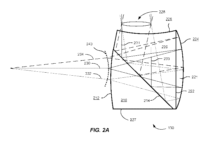
100581 FIG. 2A is a ray tracing diagram illustrating propagation of light
through the optical
assembly section according to an embodiment of the present invention. The
optical assembly
section 130 includes a prism element 210 and a collimation element 220 coupled
at an
interface. In an embodiment, the prims element and the collimation element are
optically
bonded at the interface. As described more fully herein, one or more of the
surfaces of the
optical assembly section 130 can include optical power. Thus, although
collimation of light
in terms of collimating surface 224 is discussed herein, it will be
appreciated that surfaces
other than collimating surface 224 can contribute to collimation of light by
the system. The
scanning fiber 154 in the fiber oscillation region 120 is illustrated at three
scanning positions:
on axis 230 (solid lines), off axis to the right 23.2 (dashed lines), and off
axis to the left 234
(dashed lines). As illustrated in FIG. 2A, the tip of the scanning fiber
sweeps through a
substantially spherical surface, illustrated by curve 240 in FIG. 2A, as it
oscillates, resulting
in a convex surface to be imaged, such that curve 240 can be referred to as a
convex object
surface. Conventional lenses are typically designed for flat object planes or
concave object
surfaces. Embodiments of the present invention utilize designs in which the
convex object
surface 240 associated with the tip of the scanning fiber 152 is matched with
the concave
collimating surface 224, which, at a high level, can be a substantially
spherical mirror having
twice the radius of curvature of the radius of curvature of the convex object
surface 240.
Accordingly, in some embodiments, the majority of focusing is achieved using
convex
collimating surface 224, which can be implemented as a curved mirror with an
aspheric
.. correction term. Although refractive and reflective elements are
illustrated in FIG. 2A,
embodiments of the present invention are not limited to these implementations
and diffractive
surfaces, meta-surfaces, and the like can be utilized in accordance with
embodiments of the
present invention. For example, collimating surface 224, rather than be a
reflective surface,
could be a diffractive surface, a meta-surface, or the like. One of more of
the other surfaces
illustrated in FIG. 2A can also be implemented using diffractive structures or
combinations of
diffractive and/or refractive structures. An example would be a diffractive
structure to
compensate for chromatic aberration and a refractive structure to
focus/defocus the beam.
12
CA 03056787 2019-09-16
WO 2018/175542 PCT/US2018/023505
One of ordinary skill in the art would recognize many variations,
modifications, and
alternatives.
[0059] in addition to scanning fibers, other optical systems can be utilized
to form the
convex object surface 240. Examples of these optical systems include other
waveguide
scanning systems including MEMS-based scanning systems, a scanning mirror
system with a
converging beam, a scanning point source, a flat panel display combined with
optics to create
the curved object surface, or the like.
[0060] Embodiments of the present invention enable the optical prescriptions
of the various
optical surfaces to be varied to optimize size, exit pupil diameter, combined
optical power,
linear magnification, angular magnification, distance between the exit pupil
and the output
surface, and the like. Control of the curvature of the input surface 212,
collimating surface
224 and output surface 226 enables various properties of the output beam to be
controlled,
including beam diameter, angular magnification of the angle associated with
the fiber
deflection (i.e., angle between scanning positions 232 and 234), and the like.
It should be
noted that in some implementations, beam splitter 214 can include curvature
such that it is
not a planar surface, thereby providing additional design freedom. This non-
planar shape
(i.e., non-planar curvature) can include curvature (e.g., concave or convex)
to introduce
optical power, compensate for aberrations, or the like. Additionally, the
index of refraction
of the materials used to fabricate optical assembly section 130 can be
adjusted to modify the
optical properties discussed above. Moreover, the beam splitter 214 can be a
partially
reflective (50/50 split) surface, polarizing beam splitter, a wavelength
selective beam splitter,
or the like.
[0061] Referring to FIG. 2A, a multiplexing functionality could be implemented
if the
polarizing beam splitter 214 has varying polarization, for example, as a
function of time,
alternately passing and reflecting incident light. Shutters integrated into
the optical path
between the partially reflective surface/polarizing beam splitter and the
collimating surface
224/surface 227 could be utilized to multiplex between the two optical paths.
Accordingly,
some embodiments provide a multiplexed display with a high resolution, narrow
field of view
image surrounded by a lower resolution, wide field of view image. in some
embodiments,
surface 227 could be absorbing, providing a shutter effect when light is
reflected from the
polarizing beam splitter 214 toward surface 227. One of ordinary skill in the
art would
recognize many variations, modifications, and alternatives.
13
CA 03056787 2019-09-16
= =
WO 2018/175542
PCT/US2018/023505
[00621 'Referring once again to FIG. 2A, the scanning fiber 154 acts as a
point source of
light, emitting a cone of light. These cones of light as illustrated as they
propagate from the
convex object surface 240 through the optical assembly section 130. As the
scanning fiber
sweeps through the oscillatory pattern, different pixels are illuminated to
form the desired
image. In the embodiment illustrated in FIG. 2A, the light from the scanning
fiber is
polarized so that after it enters the optical assembly section 130 though
input surface 212, it
will pass through the polarizing beam splitter 214 with little reflection,
passes through quarter
wave plate 222, and impinges on the collimating surface 224. After reflection,
the light
passes through quarter wave plate 222 a second time and reflects off of
polarizing beam
splitter 214 toward output surface 226. Exit pupil 228 is formed outside the
optical assembly
section 130 for delivery to the eyepiece. As will be evident to one of skill
in the art, for many
optical systems, alignment between the exit pupil and the input plane of
another optical
system is preferable. Accordingly, the working distance between output surface
226 and exit
pupil 228 enables embodiments of the present invention to be utilized in
conjunction with a
wide variety of optical systems. As an example, if the light emitted by the
fiber scanning
projector is utilized by a waveguide-based optical system, the input coupling
element of the
waveguide-based optical system could be placed coincident, for example,
coplanar, with the
exit pupil 228. In an embodiment, the exit pupil 228, which provides a
location at which a.
small diameter beam is formed, can enable efficient coupling into a small
input coupling
element, which can be matched in size to the exit pupil, thereby efficiently
utilizing the area
of the waveguide-ba.sed optical system. As illustrated in FIG. 2A, the three
cones of light
emitted at each of the three illustrated positions 230, 232, and 234 of the
scanning fiber 154,
are collimated as they exit the optical assembly section as shown, for
example, by collimated
rays 231 and 233, which define the edges of the cone of light emitted at on
axis position 230.
[00631 In another particular embodiment, the polarizing beam splitter can be
replaced with
a wavelength selective beam splitter such that one or more colors would pass
through the
beam splitter while other color(s) are reflected toward surface 227, which can
be
implemented as a surface with optical power. This wavelength selectivity will
enable
focusing through the use of diffractive elements or meta-surfaces as
diffractive optics are
used as an alternative to refractive optics. Thus, embodiments of the present
invention can
integrate meta-surfaces on one or more of the input surface 212, collimating
surface 224,
surface 227, and/or output surface 226 to encode multiple lens functions into
a meta-surface
for wavelength selective optical processing, other diffractive optical
functions, dispersion
14
CA 03056787 2019-09-16
WO 2018/175542 PCT/US2018/023505
compensation, or the like. In some designs, dispersion correction is provided
by the various
surfaces, for example, dispersion compensation can be implemented by
correcting aberrations
occurring at the input surface by aberration correction provided on the output
surface.
[0064] As discussed in additional detail in relation to FIG. 2B, the quarter
wave plate can
also be fabricated by vacuum forming on the collimated surface 224. In this
implementation,
after formation of the quarter wave plate on the curved surface, a metallized
or other suitable
reflective surface could be formed to complete the fabrication of collimating
surface.
[0065] In an embodiment, the input surface 212, the collimating surface 224,
and the output
surface 226 of the optical assembly section 130 can have optical power to
compensate for
spherical aberration as well as to provide for magnification of the field of
view in some
embodiments. Accordingly, using a smaller deflection of optical fiber in the
fiber oscillation
region leads to larger field of view. As an example, the input suiface 212 can
be convex with
respect to the input light to provide positive optical power, the collimating
surface 224 can be
concave with respect to the light from the input surface to provide negative
optical power,
and the output surface can be convex with respect to light from the beam
splitter to provide
negative optical power. The collimating surface 224 is substantially
spherical, but includes
an aspheric curvature in some implementations. The aspherical curvature can
correct
spherical aberration and the overall curvature can result in collimation of
the light by the
collimating surface. The collimating surface 224 can be fabricated as a
reflective element
through the deposition of one or more reflective coatings, a metalized
coating, or the like.
[0066] It should be noted that although collimating surface 224 can have
approximately
twice the radius of curvature of convex object surface 240, which can also be
referred to as a
curved object surface, in some embodiments, this is not required by the
present invention and
the input surface 212 and the output surface 226 can incorporate optical power
in addition to
the optical power present in collimating surface 224. Thus, as additional
optical power is
implemented through input surface 212 and output surface 226, the curvature of
collimating
surface 224 can deviate from twice the curvature of convex object surface 240.
Additionally,
as discussed herein, aspherical components can be integrated into the optical
surfaces
including input surface 212, collimating surface 224, and output surface 226.
[0067] In an exemplary fabrication process, the optical assembly section 130
is fabricated
by bonding three elements together. In this process, the first element is a
prism element 210
and the second element is a collimating optic section 220 that is bonded to
the prism element.
CA 03056787 2019-09-16
=
WO 2018/175542 PCT/US2018/023505
The prism element 220 receives light through input surface 212. A polarizing
beam splitter
214 is formed at the interface of the prism element 210 and the collimating
optic section 220.
In some embodiments, a polarization selective coating is applied to the
longest surface of the
prisin prior to bonding to form the polarizing beam splitter. A quarter wave
plate 222 is
formed on the back surface of the collimating optic section 220 and a third
element
comprising a curved reflective optic 221 is bonded to the quarter wave plate.
As described
herein, the curved reflective optic 221 includes collimating surface 224,
which can be
metalized or otherwise coated to provide high reflectivity.
100681 During operation, using polarized light at the input, the majority of
the polarized
input light will pass through polarizing beam splitter 214 on a first pass,
pass through a
quarter wave plate 222, reflect and be collimated by the collimating surface
224, pass a
second time through the quarter wave plate 222 (now with an orthogonal
polarization state)
and substantially reflect from the polarizing beam splitter toward the output
surface 226.
100691 FIG. 2B is a side view of an alternative optical assembly section
according to an
alternative embodiment of the present invention. Referring to FIGS. 2A and 2B,
collimating
optic section 220 and curved reflective optic 221 illustrated in FIG. 2A have
been combined
into a single (i.e., monolithic) collimating reflector 251 to form alternative
optical section
250.. Reflective surface 252 includes a wave plate that introduces a half wave
of phase shift
upon reflection. In one implementation, a quarter wave plate is formed on the
right edge of
the collimating reflector 251 before reflective surface 252 is formed, for
example, by
depositing a metal film, a dielectric film, or the like. In other embodiments,
a microstructure
can be utilized to introduce the half wave of phase shift upon reflection.
Thus, the alternative
optical section 250 is not limited to a specific manner of implementing phase
retardation and
reflection. One of ordinary skill in the art would recognize many variations,
modifications,
and alternatives.
[0070] FIG. 2C side view of a beam splitter cube based optical assembly
section according
to an embodiment of the present invention. Beam splitter cube 261 is utilized
as the basis of
the beam splitter cube based optical assembly section 260 and additional
optical elements
262;263, and 264 are cast onto the outer surfaces of the beam splitter cube
261 to form the
input surface, the collimating surface, and the output surface, respectively.
In this
embodiment, a quarter wave plate can be implemented at the intersection of the
beam splitter
cube 261 and the optical element 263 forming the collimating surface. In an
alternative
16
CA 03056787 2019-09-16
=
WO 2018/175542
PCT/US2018/023505
embodiment, a surface 266 can be used to define the collimating surface of the
optical
element 263, resulting in alignment between the edge of optical element 263
and the surface
267 of optical element 264. In this alternative embodiment, it can be noted
that the optical
element 263 can be trimmed at the periphery to form elements with non-circular
plan views,
including rectangular plan views. Accordingly, optical element 263 has a
trimmed surface or
edge that is aligned with surface 268 of beam splitter cube 261. This
alignment between
edges of the various elements can facilitate registration during
manufacturing, including
bonding of the various elements. The use of a glass beam splitter cube 261
provides
advantages including the selection of the polarization selective coatings used
to fabricate the
beam splitter surface 265. Additionally, manufacturability is enhanced by this
design due to
the wide availability of glass beam splitter cubes, including small beam
splitters. In other
embodiments, beam splitters of materials other than glass, including plastic,
are utilized. In
addition to formation of the optical elements (e.g., refractive and reflective
optical elements)
through casting, other techniques can be utilized to achieve optical effects,
including molded
elements, traditionally fabricated optics, the use of diffractive surfaces,
and/or meta-surfaces,
and the like.
100711 FIG. 21) is a side view of another alternative optical assembly section
according to
an alternative embodiment of the present invention. In the alternative
embodiment of the
optical assembly section 270 illustrated in FIG. 2D, the polarization
selective coating utilized
for the polarizing beam splitter is removed along with the quarter wave plate.
In this
alternative embodiment, a partially reflective surface 271 (e.g., 50/50
reflector) joins the
prism element 272 to the collimating element 273. Half of the light incident
from input
surface 212 passes to collimating surface 224 and reflects back toward the
partially reflective
surface 271 joining the prism element 272 and the collimating element 273. The
other half of
the light is reflected toward reflective surface 274, which can have the same
curvature as
collimating surface 224 in this alternative embodiment. As a result, light
reflected from
collimating surface, as well as light reflected from reflective surface 274 is
collimated (given
the optical power of output surface 226). The embodiment illustrated in FIG.
21) can
improve optical efficiency since light that is reflected from reflective
surface 274 is available
for output from the optical assembly section. In an embodiment, a single exit
pupil is shared
by the light reflecting from collimating surface 224 as well as the light
reflecting from
reflective surface 274, discussed as superimposed exit pupils in relation to
FIG. 2E.
17
CA 03056787 2019-09-16
= =
=
WO 2018/175542
PCT/US2018/023505
[0072] Utilizing this design, different optical power can be achieved using
the collimating
surface 224 and reflective surface 274, which can have different curvatures,
resulting in a
zoomed in/out view, -wide/narrow field of view, and the like as light is
directed to each of
these surfaces in a multiplexed manner. As an example, the reflectivity of the
partially
reflective surface 271 could be varied to provide time-base multiplexing.
[0073] A multiplexing functionality could be implemented since the partially
reflective
surface 271 could have varying reflectivity, alternately passing and
reflecting incident light.
Shutters integrated into the optical path between the partially reflective
surface 271 and the
collimating surface 224/reflective surface 274 could be utilized to multiplex
between the two
optical paths. Accordingly, some embodiments provide a multiplexed display
with a high
resolution, narrow field of view image surrounded by a lower resolution, wide
field of view
image. One of ordinary skill in the art would recognize many variations,
modifications, and
alternatives.
[0074] In another implementation, a tiled image can be formed by tilting
partially reflective
surface 271 at an angle other than 45" with respect to the incoming light.
Light passing
through the partially reflective surface 271 will reflect from collimating
surface 224 and be
directed in a first direction after passing through output surface 226. Light
reflecting from
the partially reflective surface 271 will reflect from reflecting surface 274
and be directed in a
second direction after passing through output surface 226. Accordingly, light
reflected from
collimating surface 224 could be tilted to the left after passing through
output surface 226 and
light reflected from reflecting surface 274 could be tilted to the right after
passing through
output surface 226, thus providing inputs directed to different portions of
the image field for
tiled display implementations.
[0075] FIG. 2E is a side view of a multi-polarization tilted reflector optical
assembly
section according to an alternative embodiment of the present invention. In
this
implementation in which a polarization sensitive material forms a polarizing
beam splitter
283 at the interface of the prism element 284 and the collimating element 285,
similar to
polarizing beam splitter 214 in FIG. 2A, the input light from the fiber
scanning projector
could have two signals encoded with different polarizations. A first input
beam 286 encoded
with a first polarization could pass through the polarization sensitive
material of the
polarizing beam splitter 283 to reflect off of collimating surface 224. This
beam will form an
exit pupil 281. The second input beam 287 encoded with the second polarization
will reflect
18
CA 03056787 2019-09-16
= =
WO 2018/175542 PCT/US2018/023505
from the polarization sensitive material of the polarizing beam splitter 283
to reflect off of
reflecting surface 289. This beam will form an exit pupil 282. Because the
interface of the
prism element 284 and the collimating element 285 are tilted at an angle other
than 45' with
respect to the input beams, the exit pupils 281 and 282 can be spatially
offset. As an example
if polarizing beam splitter 283 is color selective, an exit pupil associated
with a first color
(e.g., green) can be positioned adjacent an exit pupil associated with a
second color (e.g., red)
so that the exit pupils can provide spatially separated beams for input to the
eyepiece. In
addition to the spatial separation in the z-direction as illustrated in FIG.
2E, the exit pupils
can. be spatially separated in the x-direction or the y-direction.
[0076] Accordingly, two overla.ppin.g images could be produced or, using a
tilted surface at
the interface of the prism element 284 and the collimating element 285 as
illustrated in FIG.
2E, two spatially separated images could be formed in the image field. Thus,
two laterally
separated exit pupils could be provided, which could provide input for two
input coupling
elements on waveguide displays. As discussed herein, the curvatures of
collimating surface
224 and reflecting surface 289 can be different. For example, in a wavelength
selective
implementation, a wavelength selective beam splitter could be used that would
pass a first
color to reflect from collimating surface 224. A second color would reflect
from the
polarizing beam splitter and then reflect from reflective surface 289, thereby
producing a
beam having the second color that either diverges or converges after
reflection from
reflective surface 289. This could allow, for example for spatial separation
between two
different color channels for subsequent coupling into two different incoupling
gratings, each
associated with a different waveguide layer of the eyepiece. Additionally,
these designs can
be extended to multi-depth plane implementations in which multiple beams at
each color are
utilized to provide, for example, M beams at N colors for coupling into MxN
waveguides.
The integration of quarter wave plates can be implemented in polarization
sensitive
implementations. As a result, polarization selective reflectors can be
implemented in
conjunction with spatial separation of the pupils to enable routing of one
color to a first depth
plane and routing of a second color to a second depth plane. Thus, both
wavelength
separation as well as polarization separation are included within the scope of
the present
invention.
[0077] In other embodiments, the exit pupils can be disposed at the same
location (i.e.,
superimposed). Thus, the illustration of the spatially separated pupils in
FIG. 2E is merely
one example and should not be understood to limit embodiments of the present
invention.
19
CA 03056787 2019-09-16
=
WO 2018/175542 PCT/US2018/023505
One of ordinary skill in the art would recognize many variations,
modifications, and
alternatives.
[0078] One of more of the optical surface discussed in relation to FIGS. 2A -
2E can be
variable focus and their focus can be controlled in conjunction with the input
from the fiber
scanning projector. Accordingly, rays injected into the optical assembly
section at different
angles can experience different optical powers. in this embodiment, a multi-
focal display can
be implemented as a function of field angle. Moreover, additional optical
elements can be
integrated with the structures described herein, for example, between the
output surface and
the one or more exit pupils or optically downstream of the one or more exit
pupils. These
additional optical elements, which can include relay optics, can have variable
optical power,
for example, a variable focus lens positioned between the output surface and
the one or more
exit pupils. Accordingly, collimated beams can be focused, aberration can be
corrected, other
=
optical effects can be implemented, or the like. In some embodiments, the
shape of convex
object surface 240 can vary from spherical and variable focus surfaces or
additional optical
elements can be utilized as appropriate for the curvature of the convex object
surface.
Various materials can be utilized to fabricate the structures illustrated
herein, including
materials that vary their index of refraction as a function of an applied
bias, including liquid
crystal lenses, electro-optic polymers, lithium niobate, and the like. Since
the fiber scanning
projector can be scanned at high frequencies, optical materials that can vary
their optical
properties at high frequencies are suitable for use in various embodiments. As
an example,
an optical structure that can modulate focal length rapidly can work with a
fiber scanning
projector to vary the focus on a line-by-line basis or on a pixel-by-pixel
basis. These
materials can be utilized in conjunction with the input surface and/or the
output surface of the
optical assembly section as well as in conjunction with collimating surface
224. As an
example, a deformable mirror could be integrated as an element of collimating
surface 224 or
as a replacement for reflective surface 224. Such a deformable mirror,
operating at kilohertz
rates and above, can provide variable focus operation on a line-by-line basis
or on a pixel-by-
pixel basis as appropriate to the particular application.
[0079] The maximum distance to which prism element 284 extends in the z-
direction,
marked at point A in FIG. 2E, can vary according to the particular
implementation. As
illustrated in FIG. 2E, point A is the intersection of the right side of the
collimating element
285 and the bottom of the prism element 284. The design illustrated in FIG. 2E
enables a
wide field of view as the tip of the scanning fiber sweeps through the
substantially spherical
CA 03056787 2019-09-16
= = =
WO 2018/175542 PCT/US2018/023505
surface, illustrated by curve 240 in FIG. 2A. In other embodiments, the
surface of prism
element 284 forming the right upper side of the prism element is tilted such
that point A is
moved to a reduced value in the z-direction. in a similar manner, point B can
be moved to
larger values in the x-direction as the left side of the prism element 284 is
extended and the
left side of the collimating element 285 is reduced. One of ordinary skill in
the art would
recognize many variations, modifications, and alternatives.
100801 FIG. 2F is a side view of an optical assembly including a Mangin mirror
according
to an embodiment of the present invention. Similar to one or more of the
designs discussed
above, beam splitter cube 261 is utilized as the basis of the beam splitter
cube based optical
assembly section 290. Quarter wave plate 291 is implemented at the
intersection of the beam
splitter cube 261 and the Mangin mirror 292, which provides for collimation of
the input
beam. In the illustrated embodiment, output lens 293 is implemented as an
achromatic
doublet, although other lens configurations can be utilized according to
embodiments of the
present invention.
[0081] FIG. 2G is a side view of an optical assembly including a Mangin mirror
according
to an alternative embodiment of the present invention. In the embodiment
illustrated in FIG.
2G, beam splitter cube 261 is utilized as the basis of the beam splitter cube
based optical
assembly section 294. Quarter wave plate 291 is implemented at the
intersection of the beam
splitter cube 261 and the Mangin mirror 292, which provides for collimation of
the input
beam. In the illustrated embodiment, output lens 295 is implemented as a
molded glass lens,
although other lens configurations can be utilized according to embodiments of
the present
in
100821 FIG. 2H is a side view of an optical assembly including a 31) printed
lens according
to an embodiment of the present invention. Similar to one or more of the
designs discussed
above, beam splitter cube 261 and quarter wave plate 291 are utilized in
optical assembly
section 296. An input lens 299 and an output lens 295, which can be molded
glass lenses, are
utilized in this embodiment. The collimating optic, also referred to as a
printed lens, is
formed using 3D printing, also referred to as additive manufacturing. This
collimating optic
includes a substrate 297 that supports printed lens 298, for example, a
polymer lens formed
with curvatures associated with a Mangin lens. The substrate 297 is joined to
quarter wave
plate 297, for example, using an optical adhesive.
21
CA 03056787 2019-09-16
=
WO 2018/175542 PCT/US2018/023505
[0083] it should be noted that any of the characteristics of any of the
elements and surfaces
discussed or illustrated in reference to FIGS. 2A - 2H are applicable to the
implementations
provided in any of the other implementations illustrated in FIGS. 2A - 211 as
appropriate.
Merely by way of example, curvatures of surfaces, reflective or diffractive
properties of
surfaces, polarization properties, and the like are applicable to any of the
implementations as
appropriate.
[0084] FIG. 3 is a simplified perspective view of an optical assembly section
of a fiber
scanning projector according to an embodiment of the present invention, The
optical
assembly section 130 includes prism element 210 to the collimating element
220. Light is
incident on the input surface (not shown, but facing the back left) and
propagates toward
polarizing beam splitter '214. The edge of quarter wave plate 222, collimating
surface 224,
and output surface 226 are also illustrated in this view.
[0085] In some embodiments, the fiber scanning projector can achieve a 3
arcminute
angular resolution and a 4 x 3 aspect ratio with a 500 diagonal field of view
although these
particular parameters are not required by the present invention. In some
implementations, a
60' x 30' elliptical field of view is achieved. In another embodiment, the
fiber scanning
projector can achieve a 2 arcminute angular resolution and a 4 x 3 aspect
ratio with a 50"
diagonal field of view. In yet another embodiment, the fiber scanning
projector can achieve a
1 arcminute angular resolution or less. One of ordinary skill in the art would
recognize many
variations, modifications, and alternatives.
[0086] In order to reduce the size and weight of the fiber scanning projector,
portions
which do not support light can be trimmed, forming a wedge shaped structure
that also
increasing packaging flexibility, particularly for integration with eyeglasses
with curved
frames.
[0087] FIG. 4 is a simplified perspective view of elements of the optical
assembly section
during fabrication according to an embodiment of the present invention. As
illustrated in
FIG. 4, first element 410 of the optical assembly section includes a
collimating optic section
412 that includes the propagation path of light after passing through the beam
splitter, the
collimating surface 2.24, and the output surface 226. Second element 420 of
the optical
assembly section includes the surface 412 of the prism on which the polarizing
beam splitter
can be formed. In this perspective view, the input surface not shown as it is
facing to the
22
=
=
CA 03056787 2019-09-16
= =
WO 2018/175542 PCT/US2018/023505
back left. Alignment features 430 are integrated into the materials and are
designed to match
corresponding alignment features (not shown) on the bottom left surface of the
first element.
[0088] In some embodiments, the second element 420 is fabricated from glass
materials to
facilitate the formation of the polarizing beam splitter at the interface of
the first element and
the second element since glass materials can be more suitable for deposition
of polarization
selective coatings than some plastic materials.
[0089] FIG. 5 is a simplified schematic diagram illustrating a fiber scanning
projector 500
according to an alternative embodiment of the present invention. As
illustrated in FIG. 5, a
scanning fiber 510 passes through an aperture 522 in mirror 520. The scanning
fiber is
illustrated at the ends of the range of motion. A collimating mirror 530
reflects light emitted
by the scanning fiber, which is then reflected from mirror 520 to provide
output beam 540.
In some embodiments, the radius of curvature of collimating mirror 530 is
twice the radius of
curvature of spherical object surface 512.
[0090] As discussed in relation to the fiber scanning projector, as the
scanning fiber 510 is
actuated by piezoelectric element 514, it sweeps out a substantially spherical
surface 512,
also referred to as a spherical object surface. Accordingly, after reflection
off of a
substantially spherical reflector having twice the radius of curvature of the
surface swept out
by the scanning fiber, light emitted from any point along the surface swept
out by the
scanning fiber will be well collimated after reflection from the substantially
spherical
reflector.
[0091] Because the base of the fiber scanner is adjacent piezoelectric element
514, the
deflection of the scanning fiber 510 at aperture 522 is small although the
deflection at the tip
of the scanning fiber is large (e.g., on the order of 20 degrees). As the beam
is emitted from
the tip of the scanning fiber, it fans out to form cone 516 of light as
illustrated in FIG. 5. The
collimation of the cone by substantially spherical reflector 530 provides a
beam with a much
larger diameter than the diameter of the scanning fiber so that the majority
of the reflected
light is reflected from mirror 520 with little light passing through aperture
522 in the return
path.
100921 In some implementations, the field of view of the fiber scanning
projector 500 is a.
function of the section of arc that scanning fiber 510 subtends during
oscillation. As an
example, if the scanning fiber sweeps through 20 degrees, the field of view of
the projector is
on the order of 20 degrees. Increases in the field of view can be accomplished
by increasing
23
CA 03056787 2019-09-16
WO 2018/175542 PCT/US2018/023505
the range of fiber oscillation. In other embodiments, magnification of the
effective field of
view is available to increase the field of view independent of the range of
fiber oscillation.
Comparing the fiber scanning projectors in FIGS. 2 and 5, whereas the field of
view
associated with fiber scanning projector 500 is maintained as a result of the
collimation -
.. resulting from reflection from reflector 530, optical assembly section 130
provides the
illustrated optical surfaces that can be used to introduce magnification that
can increase the
field of view produced by the projector. As an example, modification of the
curvature of
output surface 226 can be utilized to magnify the field of view.
[9093] As illustrated herein, embodiments of the present invention utilize
designs that are
.. related through the use of a spherical object plane and a corresponding
reflector having a
curvature on the order of twice the curvature of the spherical object plane.
[0094] FIG. 6A illustrates a fiber scanning projector according to an
alternative
embodiment of the present invention. The fiber scanning projector 600 in FIG.
6A includes a
scanning fiber 610 passing through and mechanically coupled to a piezoelectric
element 605,
.. a first polarization sensitive reflector 6.20, arid a second polarization
sensitive reflector 630.
A quarter wave plate 622 is integrated with the first polarization sensitive
reflector.
[0095] In operation, light emitted by the scanning fiber 610 has a
polarization that passes
through the first polarization sensitive reflector 620 and the quarter wave
plate 622. The
second polarization sensitive reflector 630 reflects the incident light, which
makes a second
pass through the quarter wave plate 622 and, as a result, is reflected from
the first polarization
sensitive reflector 620 since the polarization of the light is now oriented in
the orthogonal
direction. After reflection from the first polarization sensitive reflector
620, the light passes
through second polarization sensitive reflector 630 as an output beam 640. .As
illustrated in
FIG: 6A, the second polarization sensitive reflector 630 is curved with a
curvature that
collimates the light emitted by the scanning fiber 610. As a result, the input
beam, which was
diverging, is converted to an output beam that is collimated.
[0096] Although the optical elements illustrated in FIG. GA are illustrated as
separated by
air gaps, for example, the first polarization sensitive reflector 620 and the
second polarization
sensitive reflector 63.0 separated by air gap G, this is not required by the
present invention.
.. As an example, a solid laminated component can be utilized that includes
the first
polarization selective reflector, the quarter wave plate, and the second
polarization selective
reflector and receives light from the scanning fiber, transmits the light to a
laminated curved
24
CA 03056787 2019-09-16
=
WO 2018/175542 PCT/US2018/023505
reflector, performs polarization rotation, and then reflects light from the
first polarization
selective reflector. Thus, solid elements that can also include optical power
can be utilized to
provide for focusing/defocusing, of light as well as aberration correction.
[0097] FIG. 6B is an alternative fiber scanning projector according to an
embodiment of
the present invention. The fiber scanning projector 601 illustrated in FIG. 6A
shares some
similarities with the fiber scanning projector 600 illustrated in FIG. 6A and
the description
provided in relation to FIG. 6A is applicable to the fiber scanning projector
601 illustrated in
FIG. 6B as appropriate.
[0098] Referring to FIG. 613, the fiber scanning projector 601 includes a
scanning fiber
610,. a first polarization sensitive reflector 621 that is curved to provide
for collimation and a
second polarization sensitive reflector 631 that is substantially planar. A
quarter wave plate
is integrated with the first polarization sensitive reflector.
[0099] In operation, light emitted by the scanning fiber 610 has a
polarization that passes
through the first polarization sensitive reflector 621 and the quarter wave
plate. The second
polarization sensitive reflector 631 reflects the incident light, which makes
a second pass
through the quarter wave plate and, as a result, is reflected from the first
polarization
sensitive reflector 621 since the polarization of the light is now oriented in
the orthogonal
direction. After reflection from the first polarization sensitive reflector
621, which collimates
the light during reflection, the light passes through second polarization
sensitive reflector 631
as an output beam 640. Comparing FIGS. 6A and 6B, the folded optical path
illustrated in
FIG, 6A can be replaced with a potentially shorter optical path as illustrated
in FIG. 613, but
with common features of collimation.
[0100] FIG. 6C is another alternative fiber scanning projector according to an
embodiment
of the present invention. The fiber scanning projector 602 illustrated in FIG.
6C shares some
similarities with the fiber scannin.g projector 500 illustrated in FIG. 5 and
the fiber scanning
projector illustrated 600 in FIG. 6A and the description provided in relation
to FIGS. 5 and
6A is applicable to the fiber scanning projector 602 illustrated in FIG. 6C as
appropriate.
[0101] In the embodiment illustrated in FIG. 6C, scanning fiber 610 passes
through an
aperture 652 in curved mirror 650. A polarization selective reflector 654
reflects light during
a first pass toward the curved mirror 650. By integrating a quarter wave plate
in the optical
path, light, after reflection and collimation from curved mirror 650 passes
through the
CA 03056787 2019-09-16
= =
WO 2018/175542 PCT/US2018/023505
polarization selective reflector 654 during the second pass. The embodiment
illustrated in
FIG. 6C enables a compact configuration in a hybrid design.
[0102] As illustrated by optional lens 656, embodiments of the present
invention enable
additional optical elements to be placed a significant distance from the
elements making up
the fiber scanning projector. In this example, the distance D between the
surface of the
polarization selective reflector 654 and the lens 656 provides a working
distance that is
suitable, for example, to insert a field of view magnifier. In addition, a
spherical aberration
corrector could be inserted given the suitable, extended working distance
provided by this
embodiment.
[0103] FIG. 6D is yet another alternative fiber scanning projector according
to an
embodiment of the present invention. The fiber scanning projector illustrated
in FIG. 61)
shares some similarities with the fiber scanning projector 500 illustrated in
FIG. 5 and the
fiber scanning projector illustrated in .FIG. 6A and the description provided
in relation to
FIGS. 5 and GA is applicable to the fiber scanning projector 603 illustrated
in FIG. 6D as
appropriate.
[0104] Referring to FIG. 6D, scanning fiber 610 passes through an aperture 662
in a planar
mirror 660. A curved polarization selective reflector 664 reflects light
during a first pass
toward the planar mirror 660. By integrating a quarter wave plate in the
optical path, light,
after reflection from and collimation by the curved polarization selective
reflector 664 and
planar mirror 660, passes through curved polarization selective reflector 664
during the
second pass. The embodiment illustrated in FIG. 6D also enables a compact
configuration in
a hybrid design.
[0105] FIG. 7A is a schematic diagram illustrating a lensed fiber tip
according to an
embodiment of the present invention. As illustrated in FIG. 7A, the optical
fiber 710 includes
cladding 712 and fiber core 714. The optical fiber can be considered as a
point light source
emitting rays along an emission cone 716. In the embodiment illustrated in
FIG. 7A, the
point light source is illustrated as recessed within the core in the
longitudinal direction. A
shallow lens surface 718 can be applied to the end of optical fiber as
illustrated. The lens
surface 718 can be fabricated in a variety of different manners. As an
example, a process
utilizing focused ion beam (FIB) milling can be used to make a low stroke lens
that provides
for aberration correction as illustrated in FIG. 7A. In some embodiments, the
lens surface
718 is formed directly on the fiber tip, whereas, in other embodiments, a mold
is fabricated
26
CA 03056787 2019-09-16
=
WO 2018/175542 PCT/US2018/023505
and the lens is formed separately from the fiber tip and then bonded to the
fiber tip. One of
ordinary skill in the art would recognize many variations, modifications, and
alternatives.
[0106] The curvature of the lens surface 718 can be selected to remove
spherical aberration
resulting from optical surfaces in the system, including spherical aberration
associated with
collimating surface 224 illustrated in FIG. 2A, as well as with other
surfaces. Accordingly,
through the combination of aberration correction provided by lens surface 718
and other
surfaces, high image quality is provided by embodiments of the present
invention. Utilizing
scanning fiber designs as discussed herein, it is possible to perform optical
correction on per
pixel basis in addition to performing optical correction on a display wide
scale.
101071 FIG. 7B is a schematic diagram illustrating a lensed fiber tip
according to another
embodiment of the present invention. in addition to aberration correction,
embodiments of
the present invention enable focusing of light emitted from the fiber tip as
illustrated through
the use of positive lens 720 illustrated in FIG. 713. Lens 720 can be
fabricated directly on the
fiber tip, for example, using an FIB milling process or can be molded
separately from the
fiber tip and then bonded to the fiber tip. Emission cone 722 is focused by
lens 720 to form
focused cone 724 in this example. The strength of lens 720 may be such that
light is not
focused, but the spread of the rays associated with emission cone 722 is
reduced.
[0108] FIG. 7C is a schematic diagram illustrating a lensed fiber tip
according to an
alternative embodiment of the present invention. In addition to aberration
correction and
focusing, embodiments of the present invention enable defocusing of light
emitted from the
fiber tip as illustrated through the use of negative lens 730 illustrated in
FIG. 7C. Lens 730
can be fabricated directly on the fiber tip, for example, using an FIB milling
process or can be
molded separately from the fiber tip and then bonded to the fiber tip.
Emission cone 732 is
defocused by lens 730 to form diverging cone 734 in this example. Thus, some
embodiments
enable the numerical aperture to be increased via the use of a diverging lens
on the fiber tip.
[0109] in contrast with conventional optical systems, for example, imaging a.n
LCD into an
image plane, which are constrained by the Lagrange invariant that maintains
the optical
invariant as a constant throughout the system, fiber scanning systems can
modify the
characteristics of the pixel and change the spot size emitted by the fiber. By
use of the lenses
illustrated in FIGS. 7B and 7C, modification of the pixel size can be
accomplished, for
example, effectively reducing the mode field diameter by increasing the
numerical aperture,
decreasing the pixel size, and decreasing the imaged spot size.
27
CA 03056787 2019-09-16
WO 2018/175542 PCT/US2018/023505
[01101 The optical effects illustrated in FIGS. 7A - 7C can be combined, for
example, to
provide a lens tip that corrects spherical aberration and focuses emitted
light, corrects
spherical aberration and defocuses emitted light, corrects spherical
aberration while providing
a lens with a convex region near the fiber core and a concave re0on near the
periphery of the
fiber, and the like. One of ordinary skill in the art would recognize many
variations,
modifications, and alternatives.
101111 It is also understood that the examples and embodiments described
herein are for
illustrative purposes only and that various modifications or changes in light
thereof will be
suggested to persons skilled in the art and are to be included within the
spirit and purview of
this application and scope of the appended claims.
28