Note : Les descriptions sont présentées dans la langue officielle dans laquelle elles ont été soumises.
CA 03058293 2019-09-27
WO 2018/202774 PCT/EP2018/061343
SMART CARDS WITH METAL LAYER(S) AND METHODS OF MANUFACTURE
TECHNICAL FIELD
The disclosure relates broadly to RFID devices including "Smartcards" or
"Payment Objects" (or
"payment devices") such as plastic bank cards, plastic metal hybrid cards,
metal embedded cards,
metal veneer cards, full metal cards, RFID enabled SIM cards (or payment
cards, electronic tickets,
electronic identification cards, chip cards and the like), wearable devices
(activity trackers, watches,
smart jewelry, wristbands, bangles, cuffs, bracelets, talisman charms,
lockets, rings and the like) and
accessories (payment sliders, key-fobs, money clips, wallets and the like)
having RFID (radio
frequency identification) chips or chip modules (CM) capable of operating in a
"contactless" mode
(ISO 14443 or NFC/ISO 15693), including dual interface (DI) smartcards and
payment objects (or
payment devices) which can also operate in "contact" mode (ISO 7816-2). Some
of the disclosure(s)
herein may relate to smartcards having only a contact interface.
The disclosure may relate to coupling frames that are tuned to resonant at a
certain ISM frequency.
The disclosure relates to Antenna Modules (AM), Transponder Chip Modules
(TCMs), Coupling
Frames (CFs), Stacks of Coupling Frames (SCFs), Coupling Frame Antennas
(CFAs), including
Transponders in general and Transponder Chip Modules with integrated Coupling
Frame (CF),
suitable for implanting, embedding, insertion or placement in smartcards,
metal housings, metal
casing, metal plates, jewelry pieces, tokens, tags or for mechanical and
electrical connection to a
loop(s) of wire or spiral of wire such as a charm bracelet for use in all
payment and identification
applications.
The techniques disclosed herein may also be applicable to RFID devices
including "non-secure
smartcards and tags" such as contactless cards in the form of keycards, medic-
alert tags, access control
cards, security badges, key-fobs, wearables, mobile phones, tokens, small form
factor tags, data
carriers and the like operating in close proximity with a contactless reader.
This disclosure may also relate to the design and use of laser or chemically
etched planar antennas in
transponders, tags, transponder chip modules (TCMs) or antenna chip modules
(AM).
This disclosure may also relate to Inductive Coupling (IC) between a
Transponder Chip Module
(TCM) or an RFID chip connected to an antenna (e.g. in general a Tag,
Transponder, Transponder
Chip Module) and a Coupling Frame (CF), a Stack of Coupling Frames (SCFs), or
Overlapping
Coupling Frames (0CFs) when in the presence of an electromagnetic field
generated by a contactless
reader or terminal, with the antenna structure of the transponder device
overlapping a slit or slits (or
CA 03058293 2019-09-27
WO 2018/202774 PCT/EP2018/061343
discontinuities) provided in the Coupling Frame (CF), a Stack of Coupling
Frames (SCFs) or
Overlapping Coupling Frames (0CFs). The Coupling Frame(s) may be made of a
solid metal
structure, a metal foil, or a conductive layer which is not electromagnetic
transparent. The slit or a
combination of slits which overlap the antenna structure of the transponder
device concentrates surface
eddy (Foucault) current density, to provide power delivery to the RFID chip.
This disclosure may also relate to the use of an inductive or capacitive
device (inductor or capacitor)
connected to a coupling frame in order to effect a controlled change in the
resonance characteristics of
a coupling frame.
The disclosure may also be applicable to coupling frames in card bodies,
wearables, jewelry and
accessories.
The disclosure may further relate to pre-laminated metal (aka "Metal Prelam"),
pre-laminated plastic-
metal or plastic-metal-plastic inlays having an array of card body positions.
The disclosure may also relate to contactless metal smartcards comprising
metal laminated layers with
a print enhancement coating disposed on the outer surfaces for direct digital
printing on metal.
BACKGROUND
A smartcard is an example of an RFID device that has a transponder chip module
(TCM) or an
antenna module (AM) disposed in a card body (CB) or an inlay substrate.
The antenna module (AM) or antenna chip module, which may be referred to as a
transponder chip
module (TCM) may generally comprise:
= a module tape (MT) or chip carrier tape (CCT), more generally, simply a
support "substrate";
= an RFID chip (CM, IC) which may be a bare, unpackaged silicon die or a
chip module (a die
with leadframe, interposer, carrier or the like), typically disposed on a
"face-down side" or
"bond side" or "chip side" (or surface) of the module tape (MT);
= the RFID chip may have an antenna integrated therein, but generally a
module antenna (MA)
is typically required to effect contactless communication between the RFID
chip and another
RFID device such as an external contactless reader;
= a module antenna (MA) or antenna structure (AS), typically disposed on
the same face-down
side of the module tape (MT) as the RFID chip (IC), and connected therewith,
for
implementing a contactless interface, such as ISO 14443 and NFC/ISO 15693 with
a
contactless reader or other RFID device.
2
CA 03058293 2019-09-27
WO 2018/202774 PCT/EP2018/061343
When operating in a contactless mode, a passive antenna module (AM) or
transponder chip module
(TCM) may be powered by RF from an external RFID reader, and may also
communicate by RF with
the external RFID reader.
A dual-interface antenna module (AM) or transponder chip module (TCM) may also
have a contact
pad array (CPA), typically comprising 6 or 8 contact pads (CP, or "ISO pads")
disposed on a "face-up
side" or "contact side" (or surface) of the module tape (MT), for interfacing
with a contact reader in a
contact mode (ISO 7816). A connection bridge (CBR) may be disposed on the face-
up side of the
tape for effecting a connection between two components such as the module
antenna and the RFID
chip on the other face-down side of the module tape.
A conventional antenna module (AM) or transponder chip module (TCM) may be
generally
rectangular, having four sides, and measuring approximately 8.2 mm x 10.8 mm
for a 6-contact
module and 11.8 mm x 13.0 mm for an 8-contact module. As disclosed herein, a
generally rectangular
transponder chip module (TCM) may have a larger or smaller form factor than a
conventional
transponder chip module (TCM). Alternatively, the transponder chip module
(TCM) may be round,
elliptical, or other non-rectangular shape.
A module antenna (MA) may be disposed on the module tape (MT) for implementing
a contactless
interface, such as ISO 14443 and NFC/ISO 15693. Contact pads (CP) may be
disposed on the module
tape (MT) for implementing a contact interface, such as ISO 7816.
A planar antenna (PA) structure, or simply "planar antenna (PA)", whether
chemically-etched (CES)
or laser-etched (LES), is a type of antenna structure (AS) and may comprise a
long conductive trace or
track having two ends, in the form of a planar, rectangular spiral, disposed
in an outer area of a module
tape (MT), surrounding the RFID chip on the face-down side of the module tape.
This will result in a
number of traces or tracks (actually, one long spiraling trace or track),
separated by spaces (actually,
one long spiraling space). The track (or trace) width may be approximately 100
m. The planar
antenna may be fabricated on other than the module tape, such as on a separate
substrate, and joined to
the module tape.
US 8,672,232 discloses a card which includes a first assembly comprised of
multiple plastic layers
attached via an adhesive to a metal layer. The multiple plastic layers forming
the first assembly are
laminated under a first selected temperature and pressure conditions to
preshrink the multiple plastic
layers, stress relieve the first assembly and render the first assembly
dimensionally stable. The
laminated first assembly is then attached to a metal layer via an adhesive
layer to form a second
assembly which is then laminated at a temperature below the first selected
temperature to form a card
which is not subjected to warpage and delamination. Claim 1 therein describes:
3
CA 03058293 2019-09-27
WO 2018/202774 PCT/EP2018/061343
A method of making a card comprising the steps of:
forming a first assembly of a first predetermined thickness, said first
assembly including at
least two layers of plastic material;
firstly laminating the at least two layers of different plastic material at a
first predetermined
temperature and pressure for forming said first assembly;
wherein said first lamination step comprises preshrinking the at least two
layers of plastic
material and reducing subsequent dimensional changes of the layers forming the
first
assembly;
secondly forming a second assembly including said first assembly and a metal
layer with an
adhesive layer between the first assembly and the metal layer; and
laminating the second assembly at a temperature which is lower than the first
predetermined
temperature.
Claim 11 therein describes:
A card comprising:
a first assembly comprised of multiple plastic layers which wherein the
multiple plastic
layers have been laminated at a first temperature and pressure to preshrink
the layers and
reduce their subsequent dimensional changes;
said first assembly having an inner surface and an outer surface; the outer
surface defining
one of the top and bottom side of the card;
a layer of metal material and an adhesive layer; the layer of metal material
having an inner
surface and an outer surface;
the inner surface of the layer of metal material being attached to the inner
surface of the first
assembly via said adhesive layer, the combination of said first assembly,
adhesive layer and
the metal layer forming a second assembly which is laminated at a temperature
which is less
than the first temperature, and wherein the outer surface of the layer of
metal material defines
the other one of the top and bottom side of the card.
Smartcard Construction
A typical smartcard includes multiple layers of white plastic made from
polyvinyl chloride (PVC) with
a clear PVC layer on top. Standard PVC films (homo-polymer) have a VICAT
softening point at 76 C.
The top transparent layer is referred to as an overlay and can be made of a
different material film to
PVC, such as a polycarbonate-based material (laser engravable). The overlay
film usually has a
backside coating of polyamide hotmelt, but the overlay can also be uncoated.
The overlay protects the
surface artwork and increases the card's shelf life. An overlay is required
for cards with security
4
CA 03058293 2019-09-27
WO 2018/202774 PCT/EP2018/061343
features and/or magnetic stripes, and must be used with full-face foil cards.
The card construction may
comprise synthetic plastic materials such as ABS, PC, PVC, PETG, polyester,
etc.
Observations Concerning US 8,672,232
In the teachings of US 8,672,232, there is no mention made that the first
plastic assembly could be a
single layer. Wherein the single plastic layer is laminated at a temperature
and pressure to preshrink
the layer and reduce its subsequent dimensional change. This preshrinking
procedure of the single
plastic layer could be performed prior to printing of the artwork.
In the teachings of US 8,672,232, there is no mention made of having multiple
metal layers, for
example two metal layers, in which the first plastic assembly is laminated to
a first metal layer, and
separately, a second plastic assembly is laminated to a second metal layer. In
a final step, the first
plastic metal layer is adhesively attached to the second plastic metal layer.
In the teachings of US 8,672,232, there is no mention made that a single
plastic layer or two plastic
layers with opposing grain direction could be laminated to a metal layer to
facilitate the preshrinking
process, before laminating or adhesively attaching the artwork layer und
overlay layer to the metal
plastic assembly.
In the teachings of US 8,672,232, there is no mention made that the degree of
shrinkage of the
polymer layer(s) is directly related to the size of the sheets being
laminated. In other words, the
smaller the sheet size the lesser the effect of shrinkage. Equally, the size
and thickness of the metal
layer being laminated to the plastic layer has an influence on the transfer of
heat and the ultimate
shrinkage of the plastic layer, conversely, the smaller the metal layer the
greater the control over the
shrinkage of the plastic layer.
In the teachings of US 8,672,232, there is no mention made that the first
assembly layer shrinks
greater in the grain direction than the other direction.
In the teachings of US 8,672,232, there is no mention made that the plastic
assembly layer(s) could be
dimensionally different to the size of the metal sheet.
In the teachings of US 8,672,232, there is no mention made that the metal
sheet with the upper and
lower plastic assemblies used to form cards could be punched out from the
laminated stack-up.
Instead, "the first assembly is then attached via an appropriate adhesive to a
sheet of metal material to
form a second assembly. The second assembly is then laminated at a second
temperature which is
lower than the first temperature to form a laminated 'metal plastic" sheet
which can then be cut to
form individual cards. The individual cards may be subsequently personalized.
CA 03058293 2019-09-27
WO 2018/202774 PCT/EP2018/061343
In the teachings of US 8,672,232, there is no mention made that the final
lamination process to
assembly the card body could be performed on a single card stack-up
construction, instead of a "metal-
plastic" sheet.
In the teachings of US 8,672,232, there is no mention made that the final
lamination process to
assembly the card body could be performed on a single card stack-up
construction, using a slightly
oversized card format, instead of a "metal-plastic" sheet. In a subsequent
process the edges of the
laminated oversized card stack-up could be milled, trimmed or otherwise
adjusted to bring the
dimensions of the laminated oversized card stack-up to the desired value.
In short, US 8,672,232 describes two plastic layers laminated at a first
temperature, then laminated
with an adhesive layer to a metal layer at a second temperature (lower than
the first).
Some options (alternatives, different constructions) proposed in the
embodiments of this invention
may include the following:
1. One plastic layer, other layers could be made of a metal foil (holofoil),
paper, fleece, etc.
2. Only one laminating step
3. There are two laminating steps, but the second step (overlays) may have the
same or a higher
temperature than the first laminating step
4. Laminate at least one plastic layer to at least one metal layer to create a
clad ("prelam", or
"core", or subassembly "SAS") then laminate outer layers to at least one of
the front and back
of the clad. The outer layers may comprise a printed layer and an overlay.
Outer layers
disposed on the front of the clad may be referred to as "front (face)
subassembly", outer layers
disposed on the rear of the clad may be referred to as "back
(face)subassembly". The outer
layers (front and/or rear face subassemblies) are typically card-size (having
outer dimensions
the same as the overall card). Some inner metal layers of the card may have
outer dimensions
smaller than those of the overall card.
In a one laminating step, the front clear overlay layer, the front printed
plastic layer, an adhesive layer,
the core metal layer, an adhesive layer, the rear printed plastic layer and
the rear clear overlay layer
(with magnetic stripe) are laminated together in one step at a defined
temperature and pressure. The
core metal may consist of two metal layers adhesively attached together prior
to the one step
lamination process with the plastic layers.
Other considerations are larger graphics to compensate for shrinkage, revised
lamination processes to
control cold and hot lamination cycles with modified duration times and
pressure, and the type of
lamination plates.
6
CA 03058293 2019-09-27
WO 2018/202774 PCT/EP2018/061343
Some alternate constructions may be described hereinbelow, with reference to
alternate embodiments,
examples or constructions (methods for manufacturing) of smartcards, according
to the invention.
General Comment
In their various embodiments disclosed herein, a smartcard may comprise
various layers of synthetic
plastic material and metal foil. Typically, these layers have the same overall
size (54 mm x 86 mm) as
the card, with some variations as disclosed herein (some layers may be smaller
than the overall card,
some layers may initially be larger than the overall card, etc.). Each layer
may have a front surface
and a back surface. In the drawings, the front surface is typically
illustrated as the top (as viewed)
surface, and the back surface is typically illustrated as the bottom (as
viewed surface). The individual
layers may each have a thickness. Some layers may have an opening for
accepting a transponder chip
module (TCM).
SUMMARY
It is a general object of the invention to provide improved techniques for
manufacturing smartcards.
These techniques may be applicable to various sorts of smartcards, including
plastic-metal or plastic-
metal-plastic smartcards.
Generally, the invention builds upon "slit technology" wherein a metal layer
(ML) in a smartcard has a
slit (S) or non-conductive stripe (NCS) extending to or overlapping at least a
portion of a module
antenna (MA, PA) of a transponder chip module (TCM). The slit (S) enables the
metal layer (ML) to
function as a coupling frame (CF), enhancing (rather than attenuating)
contactless communication
between the card and an external reader. This is described, for example, in US
9475086, US 9798968,
US 15939282, US 9489613, and US 9390364.
Some metal layers may have a slit (S) or non-conductive stripe (NCS) extending
from its periphery
(outer edge) to an inner position thereof, with the slit (or NCS) arranged to
overlap at least a portion of
a module antenna of the transponder chip module, so as to function as a
coupling frame (CF).
Typically, the slit (S) will extend to an opening (MO) for the transponder
chip module (TCM).
In some instances, an edge profile of a metal layer may be such that an outer
edge of the metal layer
overlaps a module antenna, and the metal layer may function as a coupling
frame, without requiring a
slit (or module opening).
According to the invention, generally, smartcards with metal layers may be
manufactured according to
various techniques disclosed herein. One or more metal layers (ML) of a
smartcard stackup may be
provided with slits (S) overlapping at least a portion of a module antenna
(MA) in an associated
7
CA 03058293 2019-09-27
WO 2018/202774 PCT/EP2018/061343
transponder chip module (TCM) disposed in the smartcard so that the metal
layer functions as a
coupling frame (CF). One or more metal layers (ML, CF1, CF2, 605, 609) may be
pre-laminated with
plastic layers (AL, 608) to form a metal core or clad subassembly (SAS, 615)
for a smartcard, and
outer printed and/or overlay plastic layers may be laminated to the front
and/or back of the metal core.
Front and back overlays (OL, 602, 614) may be provided. Various constructions
of and manufacturing
techniques (including temperature, time, and pressure regimes for laminating)
for smartcards are
disclosed herein.
According to some embodiments (examples) of the invention, a method of
manufacturing a smartcard
having a card body may be characterized by: providing a portion of the card
body as a subassembly
having two metal layers and a dielectric layer disposed between and joined by
laminating to the two
metal layers. The method may further comprise providing front and back
overlays for the
subassembly; and laminating the overlays to the subassembly to form a card
body for the smartcard.
In the method,
in a first laminating step, the subassembly of two metal layers and a
dielectric layer may be
laminated at a first temperature; and
in a second laminating step, the front and back overlays may be laminated to
the subassembly at
the same or at a higher temperature than the first laminating step.
Alternatively, in the method, the subassembly and front and back overlays may
all be laminated in a
single process step.
Front and back printed core layers (PCL) may be provided between the front and
back overlays,
respectively, and the subassembly; and laminating the front and back printed
core layers may be
laminated together with the front and back overlays.
At least one of the metal layers may have a slit (S) or non-conductive stripe
(NCS) extending from an
outer edge of the metal layer to an inner position thereof, and the slit (S)
may be disposed to overlap at
least a portion of a module antenna (MA) of a transponder chip module (TCM)
disposed in the
smartcard.
According to some embodiments (examples) of the invention, a smartcard may
comprise: a
subassembly (SAS) comprising at least one metal layer (ML) having a slit (S)
or non-conductive stripe
(NCS) extending from an outer edge of the metal layer to an inner position
thereof, and the slit (S)
may be disposed to overlap at least a portion of a module antenna (MA) of a
transponder chip module
(TCM) disposed in the smartcard; and may be characterized by: at least one
plastic layer (OL)
8
CA 03058293 2019-09-27
WO 2018/202774 PCT/EP2018/061343
including an adhesive layer (AL) laminated to at least one side of the metal
layer to form a card body
for a smart card capable of contactless communication.
The subassembly (SAS) may comprise: two metal layers (ML, CF1, CF2); and a
dielectric layer (AL)
disposed (sandwiched) between and joined to the two metal layers. Inner
plastic layers (IPL) may be
disposed on outer surfaces of the metal layers.
There may be only one metal layer, and it may be disposed at the front surface
of the card.
In some of the embodiments disclosed herein, a capacitor (CAP) may be
connected across the slit (S).
According to some embodiments (examples) of the invention, a smartcard may
comprise: a metal layer
(ML2) formed as a single turn closed loop antenna having an edge feature so
that a module antenna of
a transponder chip module (TCM) disposed in the smartcard overlaps one or more
inner or outer edge
positions on the continuous closed circuit loop antenna.
According to an embodiment (example) of the invention, a method of
manufacturing metal hybrid
smartcards from pre-laminated metal core inlays may comprise: providing a
front subassembly by
joining (or collating) a front clear overlay layer and a front printed layer
having a conventional sheet
format of 2 x 8 card body sites; providing a rear subassembly by joining (or
collating) a rear clear
overlay layer and a rear printed layer with the same sheet format; providing a
metal layer having
openings at each site in an identical format ( 2 x 8) for accepting a portion
of a chip module; providing
synthetic plastic layers with adhesive backing or adhesive layers and
synthetic plastic layers on both
sides of the metal layer, and in a first process step laminating the synthetic
plastic layers and adhesive
layers (front and back) to the metal core to form a pre-laminated metal inlay,
with the synthetic plastic
layers on both sides of the metal core shrinking under the influence of
pressure and temperature; And
in a second process step laminating the front and rear subassemblies against
the pre-laminated metal
inlay to form the complete card stack-up construction, with minimum shrinkage
of the front and rear
printed layers. A slit (S) or a non-conductive stripe (NCS) may be provided
extending from the
opening in the metal layer at each inlay site to a position beyond the
periphery edge of each card body
in the 2 x 8 array, so that the metal layer in the final card body functions
as a coupling frame for a
contactless interface. A plastic slug may be disposed in the recess opening at
each site in the metal
inlay prior to pre-lamination. In a third process step, a card body from each
site is mechanically
removed (milling, wire eroding, punching, etc.) from the final laminated sheet
with metal core. A
recess area may be milled through the front subassembly and into the plastic
slug for accepting the
chip module. A magnetic strip may be included in the rear plastic subassembly.
The smart card may
be a "Plastic-Metal-Plastic" Hybrid Card.
9
CA 03058293 2019-09-27
WO 2018/202774 PCT/EP2018/061343
According to an embodiment (example) of the invention, a method of
manufacturing metal hybrid
smartcards also known as metal embedded smartcards from a metal core inlay
having a single or
multiple metal layers may comprise: providing a front subassembly by joining
(or collating) a front
clear overlay layer and a front printed layer having a conventional sheet
format of 2 x 8 card body
sites; providing a rear subassembly by joining (or collating) a rear clear
overlay layer and a rear
printed layer with the same sheet format; providing a metal core inlay having
as option openings at
each site in an identical format ( 2 x 8) for accepting a portion of a dual
interface chip module;
providing an adhesive layer on both sides of the metal core inlay, and in a
one laminating step: the
synthetic plastic layers and adhesive layers (front and back) to the metal
core inlay are laminated
together to form the complete card stack-up construction, with minimum
shrinkage of the front and
rear printed layers. A slit (S) or a non-conductive stripe (NCS) may be
provided extending from the
intended position of the dual interface chip module at each inlay site, or
from an opening in the metal
layer at each inlay site, to a position beyond the periphery edge of each card
body in the 2 x 8 array, so
that the metal core in the final card body functions as a coupling frame for a
contactless interface. In a
final process step, a card body from each site is mechanically removed
(milling, wire eroding,
punching, etc.) from the plastic laminated layers with metal core. A recess
area may be milled through
the front subassembly for accepting the dual interface chip module. A magnetic
strip may be included
in the rear plastic subassembly. The metal core inlay may comprise of two
metal layers with slits
separated by an adhesive coated dielectric layer. The adhesive coated layer
may be sprayed or silk
screen printed to minimize its thickness. The smartcard may be a "Plastic-
Metal-Plastic" Hybrid Card
or Metal Embedded Card.
According to an embodiment (example) of the invention, method of making
plastic-metal-plastic
smartcards having a metal core or metal face laminated to one or more layers
of plastic may comprise:
performing a cycle of heating one or more of the plastic layers to a value Tla
above their Tg or Vicat
temperatures, and then cooling the plastic layers; and repeating the cycle at
alternate temperatures
T lb, Tic, etc. The cycle of heating and cooling may be performed under
pressure with the plastic
layers in sheet form, roll-to-roll, or on coils of plastic material bearing
optional spacer layers to
prevent sticking of layers to each other. Following thermal cycling, the
plastic layers may be trimmed
to a required shape or size. Following thermal cycling, the plastic layers may
be printed. The plastic
layers may comprise Polyvinyl Chloride (PVC), Polycarbonate (PC), Polyethylene
terephthalate (PET)
or Polyethylene Terephthalate Glycol-modified (PET-G). Different layers may
comprise different
plastic materials.
According to an embodiment (example) of the invention, a method of
manufacturing metal veneer
smartcards from pre-laminated metal inlays may comprise: providing a metal
sheet with a thickness of
550 [tin in an inlay format, 2 x 8, 4 x 8, 2 x 7, 4 x 7, etc., having an array
of card body positions with
CA 03058293 2019-09-27
WO 2018/202774 PCT/EP2018/061343
each site prepared with: a window (13.1 mm x 11.9 mm, depth ¨ 250 [tin and a
lip of 1.3 mm) to
accept the implant of a chip module and an opening (9.5 mm x 8.5 mm) in the
metal to accommodate
the mold mass of the chip module, a laser defined slit (with a width of ¨100
[tin or less at the front
face) extending from each opening to an area beyond the periphery edge of each
card site, a recess
area (mechanically milled, eroded or chemically etched) with a depth of ¨200
[tin at each site on the
underside of the metal sheet around the area of the opening and slit leaving a
stepped frame around the
perimeter edge of the opening to enhance the mechanical strength, and stuffing
the recess area with an
adhesive backed plastic insert or non-conductive insert to re-stabilize the
area around the slit;
providing a rear adhesive layer (-75 [tin) and a synthetic plastic layer (-50
[Lin) to the underside of the
mechanically prepared metal sheet and in a first production step laminating
the sandwich to create a
pre-laminated metal inlay for metal veneer smartcards. A Mylar plastic sheet
may be attached to the
front face of the metal sheet to protect against scratches during handling and
processing. A plastic slug
may be disposed in the opening to accept a chip module at each site in the
metal inlay sheet prior to
pre-lamination. In a second production step, a rear clear overlay layer (-50
[tin) and a rear printed
layer (-125 [tin) are laminated to the pre-laminated metal inlay. Card bodies
are extracted from the
final laminated sheet and personalized.
According to another embodiment of the invention, a method of manufacturing
metal veneer
smartcards from pre-laminated metal inlays with integrated metal slugs may
comprise: providing a
front face metal sheet with a thickness of ¨200 [Lin in a suitable inlay
format having an array of card
body positions with each site prepared with: a window to accept the implant of
a chip module, a laser
defined slit extending from each window to an area beyond the periphery edge
of each card site;
providing a first adhesive layer (75 [tin) to support the attachment of a
metal slug (250 [tin) having a
defined weight at each site in the inlay format to act as a coupling frame
with a slit and module
opening; providing a plastic layer (optionally colored) with openings to
accept each metal slug to act
as a supporting frame: providing a second adhesive layer (75 [tin) and a
synthetic plastic layer (50 [tin)
to complete the inlay stack-up construction, in preparation for pre-
lamination. In a final lamination
step, an overlay layer and the printed graphics layer are laminated to the pre-
laminated metal inlay
with integrated metal slugs. The metal slug acting as a coupling frame may
have a capacitor connected
across its slit to regulate the frequency response and bandwidth of the
system.
In another embodiment of the invention, the slit in the front metal layer may
be eliminated and a
coupling frame antenna (a replacement for a booster antenna), optionally with
shielding material, is
introduced into the inlay stack- up construction to support the contactless
interface. Optionally a
capacitor can be connected across the slit (which may also be referred to as a
void or separation gap)
of the coupling frame antenna to optimize RF performance. Optionally, the
front metal layer may be
electrically connected or form an integral part of the coupling frame antenna
to create a folded
11
CA 03058293 2019-09-27
WO 2018/202774 PCT/EP2018/061343
coupling frame or 3 dimensional coupling frame. The pre-laminated metal inlay
may comprise a metal
layer with windows to accept a chip module, a recess area or areas in the
metal layer to accept the
strategic location of ferrite shielding material attached thereto with a
suitable adhesive. The inlay is
completed by addition of adhesive layers and plastic substrate layers to
create the inlay stack-up for
pre-lamination.
The coupling frame antenna in the above configurations may be referred to as a
"single loop horseshoe
antenna" with a slit/void and opening to accommodate the transponder chip
module. The slit/void may
be eliminated by changing the form of the single turn closed loop antenna
having the module antenna
of the transponder chip module overlapping one or more positions on the
continuous closed circuit
loop. In essence, the shape of the antenna may not be rectangular.
Capacitive struts running parallel to the single track or interdigitated array
may be integrated
therewith.
Alternatively, the coupling frame antenna (CFA) may be substituted (replaced)
by a metal slug
coupling frame with a recess area or areas to accept the strategic positioning
of ferrite material or
Sendust powder. In this configuration, the contactless interface operates from
the non-metal side of the
metal veneer smartcard.
In their various embodiments, the invention(s) described herein may relate to
industrial and
commercial industries, such RFID applications, payment smartcards, secure
identity cards, access
control cards, payment objects, wearable devices, smart jewelry and the like.
Other objects, features and advantages of the invention(s) disclosed herein,
and their various
embodiments, may become apparent in light of the descriptions of some
exemplary embodiments that
follows.
BRIEF DESCRIPTION OF THE DRAWINGS
Reference will be made in detail to embodiments of the disclosure, non-
limiting examples of which
may be illustrated in the accompanying drawing figures (FIGs). Some figures
may be in the form of
diagrams. Some elements in the figures may be exaggerated, others may be
omitted, for illustrative
clarity.
Any text (legends, notes, reference numerals and the like) appearing on the
drawings are incorporated
by reference herein.
12
CA 03058293 2019-09-27
WO 2018/202774 PCT/EP2018/061343
Some elements may be referred to with letters ("AM", "CES", "CF", "CM", "IPL",
"LES", "MA",
"MT", "ML", "MO", "NCS", "OL", "PCL", "S", "SAS", "TCM", etc.) rather than or
in addition to
numerals. Some similar (including substantially identical) elements in various
embodiments may be
similarly numbered, with a given numeral such as "2020", followed by different
letters such as "A",
"B", "C", etc. (resulting in "2020A", "2020B", "2020C"), and variations
thereof, and may be
collectively (all of them at once) or individually (one at a time) referred to
simply by the numeral
("2020").
The figures presented herein may show different embodiments of RFID devices,
such as metal hybrid
or metal veneer smartcards or payment objects such as wearable devices. Some
of the drawings may
omit components such as the transponder chip module or module antenna, for
illustrative clarity.
Some of the figures may show only components of an RFID device, such as
coupling frames or
plastic-metal-plastic inlays.
FIG. lA is a diagram (exploded perspective view) of a DIF "Plastic-Metal-
Plastic" Hybrid Card,
before lamination. A chip module is shown for insertion into the card.
FIG. 1B is a diagram (exploded perspective view) of an alternate construction
for a DIF "Plastic-
Metal-Plastic" Hybrid Card, before lamination. The metal core may have two
metal layers, each
with a slit emanating in opposing directions from the intended position of the
chip module.
FIG. 1C is a diagram (perspective view) of a slug for fitting in the stepped
recess of the "Plastic-
Metal-Plastic" Hybrid Cards.
FIG. 1D is a more detailed view of a chip module.
FIG. 2A is a diagrammatic view of the layers of a plastic-metal-plastic hybrid
smartcard featuring one
metal layer as part of a lamination subassembly (SAS).
FIG. 2B is a partially exploded edge-on diagrammatic view of the layers of a
plastic-metal-plastic
hybrid smartcard featuring one metal layer as part of a lamination subassembly
(SAS).
FIG. 3A is a diagrammatic view of the layers of a plastic-metal-plastic hybrid
smartcard featuring a
coupling frame (CF) with slit (S) and support panel (S) and as part of a
lamination subassembly
(SAS).
FIG. 3B is a partially exploded rear diagrammatic view of the layers of a
plastic-metal-plastic hybrid
smartcard featuring a coupling frame (CF) with slit (S) and support panel (S)
and as part of a
lamination subassembly (SAS).
FIG. 4A is a diagrammatic view of the layers of a plastic-metal-plastic hybrid
smartcard featuring a
metal core having two coupling frames (CFs) with slit (S) and module openings
(MOs) as part of a
lamination subassembly (SAS).
13
CA 03058293 2019-09-27
WO 2018/202774 PCT/EP2018/061343
FIG. 4B is a partially exploded diagrammatic view of the layers of a plastic-
metal-plastic hybrid
smartcard featuring a metal core having two coupling frames (CFs) with slit
(S) and module
openings (MOs) as part of a lamination subassembly (SAS).
FIG. 5A is a diagrammatic view of the layers of a plastic-metal-plastic hybrid
smartcard featuring a
metal core having two coupling frames (CFs), one coupling frame (CF1) with
slit (S) and module
opening (MO) and the second coupling frame (CF2) with an extended slit (S2) as
part of a
lamination subassembly (SAS).
FIG. 5B is a partially exploded close-up diagrammatic view of a plastic-metal-
plastic hybrid
smartcard featuring a metal core having two coupling frames (CFs), one
coupling frame (CFI) with
slit (S) and module opening (MO) and the second coupling frame (CF2) with an
extended slit (S2)
as part of a lamination subassembly (SAS).
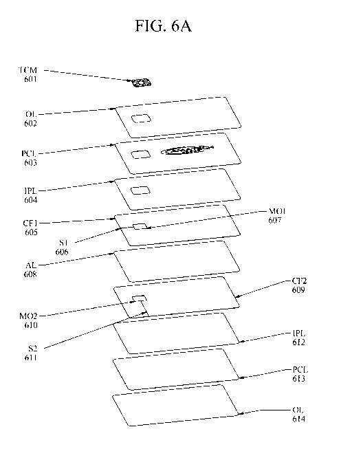
FIG. 6A is a diagrammatic view of the layers of a plastic-metal-plastic hybrid
smartcard featuring a
metal core having two coupling frames (CFs) with slit (S) and module openings
(MOs) as part of a
lamination subassembly (SAS).
FIG. 6B is a partially exploded diagrammatic view of the layers of a plastic-
metal-plastic hybrid
smartcard featuring a metal core having two coupling frames (CFs) with slit
(S) and module
openings (MOs) as part of a lamination subassembly (SAS).
FIG. 7 is a cross sectional view of a metal layer (ML) with slit (S) which has
been laminated to
adjacent layers of a smartcard stack using adhesive layers, showing a
magnified view of the region
near the slit (S).
FIG. 8A is an exploded view of a metal veneer smartcard with slit (S) on the
front metal layer (ML).
FIG. 8B is a close up of the rear side of a metal layer (ML) used in a
smartcard showing a raised
profile about the module opening designed to prevent metal warpage in the area
of a recess to
accommodate a transponder chip module (TCM).
FIG. 9 is an exploded view of a metal veneer smartcard with two metal layers
(ML) to form the core,
each functioning as a coupling frame (ML).
FIG. 10 is an exploded view of a metal veneer smartcard with two metal layers
(ML) wherein an inner
metal layer (ML) features a slit (S) and functions as a coupling frame (CF),
being
electromagnetically shielded from the first metal layer (ML) with suitably
shaped shielding
material.
FIG. 11 is an exploded diagrammatic view of a metal prelam (2 x 8 format),
with two metal layers but
no opening for the transponder chip module (TCM) at each card site.
FIG. 12 is an exploded diagrammatic view of a metal prelam (2 x 8 format),
with two metal layers and
openings for the transponder chip module (TCM) at each card site with
corresponding slugs filling
the openings.
14
CA 03058293 2019-09-27
WO 2018/202774 PCT/EP2018/061343
FIG. 13 is an exploded diagrammatic view of a laminated construction of
plastic-metal-plastic
smartcards (2 x 8 format), with two metal layers and printed graphics layers
(PGL) laminated to the
metal core layers.
FIG. 14 is an exploded diagrammatic view of a laminated construction of
plastic-metal-plastic
smartcards (2 x 8 format), comprising two metal layers and suitable plastic
layers primed to accept
direct printing of graphics onto the metal prelam.
FIG. 15 is a an exploded diagrammatic view of a metal prelam (2 x 8 format)
with three metal layers
each bearing slit arrays (SA) offset from each other, without opening for the
transponder chip
module (TCM), that may be used to produce a predominantly metal smartcard.
DETAILED DESCRIPTION
Various embodiments (or examples) may be described to illustrate teachings of
the invention(s), and
should be construed as illustrative rather than limiting. It should be
understood that it is not intended
to limit the invention(s) to these particular embodiments. It should be
understood that some individual
features of various embodiments may be combined in different ways than shown,
with one another.
Reference herein to "one embodiment", "an embodiment", or similar
formulations, may mean that a
particular feature, structure, operation, or characteristic described in
connection with the embodiment
is included in at least one embodiment of the present invention. Some
embodiments may not be
explicitly designated as such ("an embodiment").
The embodiments and aspects thereof may be described and illustrated in
conjunction with systems,
devices and methods which are meant to be exemplary and illustrative, not
limiting in scope. Specific
configurations and details may be set forth in order to provide an
understanding of the invention(s).
However, it should be apparent to one skilled in the art that the invention(s)
may be practiced without
some of the specific details being presented herein. Furthermore, some well-
known steps or
components may be described only generally, or even omitted, for the sake of
illustrative clarity.
Elements referred to in the singular (e.g., "a widget") may be interpreted to
include the possibility of
plural instances of the element (e.g., "at least one widget"), unless
explicitly otherwise stated (e.g.,
"one and only one widget").
In some figures, abbreviations (e.g., CF, S, etc.) which have been established
for devices and
components thereof may be used without accompanying reference numbers to
identify various
elements in the figures, for illustrative clarity.
In the following descriptions, some specific details may be set forth in order
to provide an
understanding of the invention(s) disclosed herein. It should be apparent to
those skilled in the art that
these invention(s) may be practiced without these specific details. In some
descriptions, parameters
CA 03058293 2019-09-27
WO 2018/202774 PCT/EP2018/061343
such as dimensions, activation distance, frequency of operation, mode of
operation and the like may be
discussed, and these should be regarded as exemplary. Any dimensions and
materials or processes set
forth herein should be considered to be approximate and exemplary, unless
otherwise indicated.
Headings (typically underlined) may be provided as an aid to the reader, and
should not be construed
as limiting.
Some processes may be presented and described in a series (sequence) of steps.
It should be
understood that the sequence of steps is exemplary, and that the steps may be
performed in a different
order than presented, some steps which are described may be omitted, and some
additional steps may
be omitted from the sequence and may be described elsewhere.
Reference may be made to disclosures of some prior patents, publications and
applications. Some text
and drawings from those sources may be presented herein, but may be modified,
edited or commented
to blend more smoothly with the disclosure of the present application.
Citation or identification of
any reference should not be construed as an admission that such reference is
available as prior art to
the disclosure.
In the descriptions that follow, metal hybrid and metal veneer smartcards (or
"metal smart cards")
operating in both contactless and contact modes may be described. It should be
understood that the
teachings set forth herein may be applicable to metal smartcards having only a
contact interface. Also,
the teachings set forth herein may be applicable to RFID devices (which may
operate only in a
contactless mode) other than metal smart cards, such as jewelry, etc.
A Production Method For Manufacturing DIF "Plastic-Metal-Plastic" Hybrid Cards
A typical smartcard may measure approximately 54 mm x 86 mm. An overall sheet
from which the
plastic layers for the cards are manufactured may comprise a plurality, such
as a 4 x 8 of card-size
areas for manufacturing a plurality (such as 32 total) of plastic layers for
the cards.
Pre-lamination may be used to offset the problem of shrinkage during final
lamination, but this may
depend on the size of the printed sheets used, i.e. the greater the sheet size
(such 4 x 8 ¨ 299 mm x
489.7mm) the greater the amount of shrinkage (e.g., in the y- and x- axes).
Also, the material plays a
pivotal role - for example, PVC shrinks more than PET or PETG.
Conventionally for a contact-only metal card, two layers of plastic material,
such as (i) an anti-scratch
overlay and (ii) a printed graphic layer may be laminated together, i.e. "pre-
laminated", before final
lamination to either side (or to both sides) of a metal core.
("Contact-only" refers to a smartcard
16
CA 03058293 2019-09-27
WO 2018/202774 PCT/EP2018/061343
having only a contact interface, and lacking a contactless interface. "Dual
interface" cards have both a
contact interface and a contactless interface.)
Card-size Lamination
As disclosed herein, at least two plastic layers, such as an overlay and a
graphic layer, may be joined
together by other than laminating, and may be referred to as a "sub-assembly"
or a "plastic layer
assembly"). A metal foil may be incorporated into the sub-assembly. These
layers (and foil) may be
different plastic materials (optionally, plus a metal foil), and may be joined
together while in sheet
form (multiple card areas). The printed plastic layer (or sheet) may be joined
to an anti-scratch overlay
film with an adhesive backing, or the layers may be collated or tacked
together with one another
(preferably outside of an area that will be printed) using an ultrasonic probe
or heat element. By
avoiding pre-lamination, there may be no pre-shrinking of the plastic layers
involved. Ultimately, the
sub-assemblies of joined plastic layers may be singulated (separated, reduced)
into several card-size
subassemblies (or plastic layer assemblies), and may be joined with a metal
layer in card size format,
and the resulting assembly (of subassemblies and metal layer) may be pre-
pressed laminated together,
before final lamination in a conventional press.
The metal core may comprise two metal layers separated by an adhesive coated
dielectric layer which
are pre-laminated together - before lamination with the plastic layers - to
produce a "Metal- Prelam".
Each metal layer in the "Prelam" may have a slit (so that the metal layer
functions as a coupling
frame) to enable contactless communication, and may have an opening to accept
the mold mass
contour of a chip module.
To avoid the problem of shrinkage, final lamination with the metal layer
(which may be a coupling
frame) will be a "card size" lamination step and not a sheet lamination
process. Therefore, there will
be no significant reduction on the overall dimensions of the plastic layers.
The techniques disclosed herein may be applicable to either (i) single
interface (i.e., contact interface)
cards, or to (ii) dual interface (i.e., contact and contactless interfaces)
cards. The metal layer (ML)
may have an opening to accommodate the mold mass of a chip module. In the case
of dual interface
cards, the metal layer may also be provided with a slit (S) extending from the
opening to an outer edge
of the metal layer so that the metal layer may function as a coupling frame
(CF).
The metal layer or coupling frame may have a stepped opening (or recess) to
accept a chip module. A
larger portion of the opening may accommodate a module tape of a chip module,
and the smaller
opening may accommodate the mold mass of a chip module.
17
CA 03058293 2019-09-27
WO 2018/202774 PCT/EP2018/061343
The opening in the metal layer may be filled with a plastic slug, plug, or the
like, for two reasons.
Firstly, during final lamination the plastic layers (printed stock and
overlays, etc.) without the slug
could (undesirably) flow into the area of the opening. Secondly, during
milling of the recess area for
the chip module, the milling tool should only touch plastic and not metal.
Since the plastic plug will
ultimately be removed or partially removed (by milling), and may not appear in
the final product, it
may be considered to be a "sacrificial" element.
To assemble the sub-assemblies and metal layer, a dry film adhesive may be
placed on both sides of
the metal layer or coupling frame. The card-size front and rear face
subassemblies (or plastic layer
assemblies) may then be pre-pressed against the adhesive layers and the metal
core or coupling frame
to form a card blank.
The resulting card blanks may be placed in a holding template (fixture) having
a format such as 3 x 8,
before final lamination in a conventional press. The cycle time for hot and
cold lamination may be
about 45 minutes.
The laminated card blanks may then be provided with a recess through the top
subassembly of two or
more plastic layers, and extending into the opening of the metal layer to
accept a chip module. As
mentioned above, the milling procedure should only be performed in the area of
the plastic slug.
After implantation of the chip module, the card blank can be personalized.
The above treatment of card-size lamination in producing dual interface metal
cards and the teachings
thereof may also be applicable to sheet format lamination. The following
diagrams of the various card
stack-up constructions may also relate to sheet lamination in a typical 2 x 8
format with the metal core
inlay (having a 2 x 8 array of card body sites) consisting of a single metal
layer or two metal layers
pre-laminated to form a "Metal-Prelam".
FIG. lA is a diagrammatic view of a DIF "Plastic-Metal-Plastic" Hybrid Card
(RFID device) 100A,
before lamination, generally comprising (from top-to-bottom, as viewed):
- an 8 pin chip module 101 which may be a transponder chip module (TCM).
The chip module may
be single interface (contact only), or dual-interface (contact and
contactless). In the latter case
(dual interface), the chip module may be a transponder chip module having a
module antenna. (A
module antenna is not required in a contact only module.) In the main, a chip
module which is a
transponder chip module will be described, as exemplary.
- a front clear overlay (plastic) layer 102 which may have a thickness of
approximately 501am. A
recess or opening (shown in dashed lines "module recess") for accepting the
module may be milled
in this layer, after final lamination.
18
CA 03058293 2019-09-27
WO 2018/202774 PCT/EP2018/061343
- a front (plastic) printed core layer 103 (displaying the logo "AMATECH")
which may have a
thickness of approximately 125 m. A recess or opening (shown in dashed lines)
for accepting the
module may be milled in this layer, after final lamination.
- the front clear overlay film with adhesive backing and front printed core
may be adhesively
attached together in sheet format and may constitute a front (plastic)
subassembly (or plastic layer
assembly, "PLA") 104.
- a layer of adhesive 106 which may have a thickness of approximately 201am
- a metal layer (ML) (or metal core) 107 which may have a thickness of
approximately 4001am and
which may be provided with an opening (MO) 109 which may be a stepped recess
extending
through the metal layer. The metal layer may have a slit S (or a non-
conductive stripe NCS) 110
extending from the opening to an outer edge thereof so that the metal layer
may function as a
coupling frame (for a contactless interface). The metal layer or core may
consist of several metal
layers with slits. The slit is not necessary for a contact only chip module.
The recess may be
stepped, having a larger portion extending 100 [tin into the metal layer, for
a module tape of the
chip module, and a smaller portion extending the rest of the way (additional
30011m) through the
metal layer for a mold mass of the chip module. This may ensure (in the case
of contactless
functionality) that the coupling frame appropriately overlaps the module
antenna of the transponder
chip module. The metal layer (ML) may comprise two metal layers, each having a
thickness of
approximately 20011m. See FIG. 1B).
- The opening MO 109 in the metal layer ML 107 may be filled with a plastic
slug 108.
- a layer of adhesive 111 which may have a thickness of approximately 201am
- a rear printed core 112 which may have a thickness of approximately 125
m. An opening or
recess for the chip module may not be required in this layer.
- a rear clear overlay 113 which may have a thickness of approximately
501am. An opening or recess
for the chip module may not be required in this layer.
- a magnetic stripe may be disposed on the bottom (as viewed) surface of
the rear clear overlay.
- the rear clear overlay film with adhesive backing and rear printed core
(including magnetic stripe)
may be attached together and may constitute a rear (plastic) subassembly (or
plastic layer
assembly, "PLA") 115.
Card-size front and rear face subassemblies (plastic layer assemblies) may be
pre-pressed against the
adhesive layers and the metal core or coupling frame to form a card blank.
Generally, the module openings (MO) of the various embodiments described
herein can be formed
(such as milled) in a final step, after lamination (pre-lam).
19
CA 03058293 2019-09-27
WO 2018/202774 PCT/EP2018/061343
FIG. 1B is a diagrammatic view of an alternate construction of a DIF "Plastic-
Metal-Plastic" Hybrid
Card (RFID device) 100B, before lamination. Generally, this embodiment differs
from that of FIG.
lA in that the single metal layer (ML) 107 having a thickness of approximately
4001am is replaced by
two metal layers (ML1, ML2) 107A, 107B each having a thickness of
approximately 20011m. There
is a layer 111 of adhesive (a dielectric medium) between the two metal layers
ML1 and ML2. More
particularly, the card may comprise (from top-to-bottom, as viewed):
- a front clear overlay (plastic) layer 102 which may have a thickness of
approximately 501am. A
recess or opening (shown in dashed lines "module recess") for accepting the
module may be milled
in this layer, after final lamination.
- a front (plastic) printed core layer 103 (displaying the logo "AMATECH")
which may have a
thickness of approximately 125 m. A recess or opening (shown in dashed lines)
for accepting the
module may be milled in this layer, after final lamination.
- the front clear overlay film with adhesive backing and front printed core
may be adhesively
attached together in sheet format and may constitute a front (plastic)
subassembly (or plastic layer
assembly) 104.
- a layer of adhesive 106 which may have a thickness of approximately 201am
- a first metal layer (ML1) 107A which may have a thickness of
approximately 2001am and which
may be provided with an opening (MO) 109A extending through the metal layer.
The metal layer
may have a slit S (or a non-conductive stripe NCS) 110A extending from the
opening to an outer
edge thereof so that the metal layer may function as a coupling frame (for a
contactless interface).
- a layer of adhesive 111 which may have a thickness of approximately 201am
- a second metal layer (ML1) 107B which may have a thickness of
approximately 2001am and which
may be provided with an opening (MO) 109B extending through the metal layer.
The metal layer
may have a slit S (or a non-conductive stripe NCS) 110B extending from the
opening to an outer
edge thereof so that the metal layer may function as a coupling frame (for a
contactless interface).
- The openings MO 109A and 109b in the metal layers ML1 107A and ML2 107B
may be aligned
with one another, and may be filled with a plastic slug 108.
- a layer of adhesive 111 which may have a thickness of approximately 201am
- a rear printed core 112 which may have a thickness of approximately 125
m. An opening or
recess for the chip module may not be required in this layer.
- a rear clear overlay 113 which may have a thickness of approximately
501am. An opening or recess
for the chip module may not be required in this layer.
- a magnetic stripe may be disposed on the bottom (as viewed) surface of
the rear clear overlay.
- the rear clear overlay film with adhesive backing and rear printed core
(including magnetic stripe)
may be attached together and may constitute a rear (plastic) subassembly (or
plastic layer assembly)
115.
CA 03058293 2019-09-27
WO 2018/202774 PCT/EP2018/061343
A sub-assembly with two metal layers and a dielectric medium (or layer)
therebetween may be
referred to as a metal "inlay". If there is one metal layer, this may be
referred to as a metal "core".
FIG. IC shows an exemplary slug 108 for fitting in the stepped recess (MO,
109). Note that the plug
resembles (but may be shorter/shallower than) a chip module, having an upper
wider portion 116
(corresponding to the module tape of a chip module) and a lower narrower
portion 117 (corresponding
to the mold mass of a chip module).
FIG. ID shows an exemplary chip module 101, which may be an antenna module
(AM) or a
transponder chip module (TCM), comprising a module tape and mold mass
encapsulating a chip. In
the case of a dual-interface (contact and contactless) chip module, which may
be referred to herein as a
transponder chip module, a module antenna may be incorporated into the chip
module.
Manufacturing a Plastic-Metal-Plastic Card
Smartcards bearing a metal core or metal face may be laminated to one or more
layers of plastic. The
layers of plastic in the card stack may comprise one or more materials
including, but not limited to,
Polyvinyl Chloride (PVC), Polycarbonate (PC), Polyethylene terephthalate (PET)
or Polyethylene
Terephthalate Glycol-modified (PET-G). The construction of such a card
typically requires the use of
thermally activated adhesives at the interfaces between the plastic layers and
metal and, optionally,
between one or more plastic layers.
A smartcard with a metal core, together with plastic or other layers, may be
assembled in a stack-up
including one or more metal layers, for lamination at a required temperature.
A challenge with this
process is that typical plastic layers used in a smartcard construction are
prone to shrinkage, plastic
egress and other dimensional changes when heated above their glass transition
temperature (Tg) or
Vicat softening temperature (e.g. Vicat B standard). For example, PET-G may
have a Vicat B
temperature of approximately 82 C. The dimensional changes that occur during
typical lamination
conditions (e.g. 120 C, 45 minutes) can result in significant distortion of
the card stack-up at the edges
of the finished card and at the locations of any cavities or voids. In
addition, in order to construct a
smartcard one or more of the plastic layers of the card may bear printed
graphics. Dimensional
changes in a printed layer of the card can result in visible distortion of the
printed graphics.
Under this aspect of the invention one or more of the plastic layers used for
smartcard construction
may be heated to a value Tla above their Tg or Vicat temperatures, and then
cooled. This process may
be repeated at alternate temperatures T lb, Tic, etc., forming a cycle. The
heating of the plastic layer(s)
may be carried out under pressure in sheet form, roll-to-roll, or on coils of
plastic material bearing
optional spacer layers to prevent sticking of layers to each other.
21
CA 03058293 2019-09-27
WO 2018/202774 PCT/EP2018/061343
The thermal cycling process results in dimensional changes in the plastic
layer(s). Following thermal
cycling the material may be trimmed back to required shape or size, the use of
thermal cycling may
ensure dimensional stability of the plastic layers during further processing
steps. At this stage one or
more layers of plastic may be printed with the graphics required for the given
smartcard design.
The dimensionally stable plastic layers can be laminated to each other and to
the metal core or face of
the smartcard. The use of adhesives with low activation temperature ensures
that the lamination
process to produce a final smartcard can be carried out a temperature T2 < Tl.
In practical terms, the pre-shrinking of the thermoplastic layers before
printing may ensure that the
plastic does not further shrink or expand during final lamination of the card
stack-up with the metal
core in a conventional press.
Selecting a front and rear plastic layer with a higher glass transition
temperature than the adhesive
layers has a significant advantage in avoiding further shrinkage or expansion
of the plastic layer
assemblies during the final lamination process.
And, contrary to the teachings of US 8,672,232, the plastic layers of the
first and second assembly can
be of the same material, for example, the printed plastic layer can be made of
polycarbonate, while the
overlay film can also be polycarbonate (laser engravable). As noted in US
8,672,232 ...
A method of making a card comprising the steps of: forming a first assembly of
a first
predetermined thickness, said first assembly including at least two layers of
plastic material;
firstly laminating the at least two layers of different plastic material at a
first predetermined
temperature and pressure for forming said first assembly; wherein said first
lamination step
comprises preshrinking the at least two layers of plastic material and
reducing subsequent
dimensional changes of the layers forming the first assembly; secondly forming
a second
assembly including said first assembly and a metal layer with an adhesive
layer between the
first assembly and the metal layer; and laminating the second assembly at a
temperature which
is lower than the first predetermined temperature.
Pre-shrinking is conventionally done in a conventional lamination press,
subjecting the plastic layers
to hot and cold cycles under extreme pressure (>20 bar). As disclosed herein,
the plastic layers may
be pre-shrunk in a belt laminator under insignificant pressure and merely
tempering the material.
Instead of a belt laminator to pre-shrink the plastic layers before printing,
a conventional lamination
press can be used.
The following materials and manufacturing steps may be utilized.
22
CA 03058293 2019-09-27
WO 2018/202774 PCT/EP2018/061343
Pre-shrinking of the Front and Rear Plastic Layer prior to Printing:
Materials
Material Layer for Printing: Polycarbonate White
Manufacturer: Bayer
Product Code: ID 4-4
Thickness: 150 microns
Material Layer for Anti-scratch Overlay Film: Polycarbonate Clear
Manufacturer: Bayer
Product Code: ID 6-2
Thickness: 50 microns
Production Step 1- Temperature Cycling
Belt Laminator Parameters for Temperature Cycling the Plastic Layers:
Temperature 125 degrees C
Pressure: 10 PSI/CM3
Speed 1.5 cm/sec
Production Step 2
Print features onto the pre-shrunk white polycarbonate (PC) to produce the
front and rear face
graphic layers
Production Step 4 -1
Lightly tack or bond the printed 150 micron PC to the back of the Clear 50
micron overlay
film with enough force from the back side of the printed layer that no imprint
on the overlay
film is visible.
Production Step 4 -2
Punch the pre-shrunk PC layers into card size plastic layer assemblies (ID1
size)
Production Step 5
Tack the adhesive layers to the back side of the front and rear plastic layer
assemblies (two
layers: Printed layer and Overlay Film).
Production Step 6 ¨ Final Lamination
Place the "card size" stack-up containing the front and rear plastic layers
assemblies, the
intermediate adhesive layers and the metal core (400 [tin) into a laminator
Lamination Parameters:
Laminate using Standard PVC setting parameters
Temperature & Pressure Settings: 140 C and 160 Bar pressure for 30 minutes.
23
CA 03058293 2019-09-27
WO 2018/202774 PCT/EP2018/061343
Use of laminated metal-plastic subassemblies (SAS)
In an alternative manufacturing process for plastic-metal-plastic smartcards a
laminated subassembly
(SAS) containing one or more sheet metal layers (MLs) may be considered. The
general concept of the
invention is the creation of a subassembly (SAS) constructed from laminated
layers of one or more
metal sheets and plastic, with appropriate adhesives where required. The
subassembly (SAS) may be
in the format of a single card or multiple cards separated from each other in
a given array. One or more
of the plastic layers of the subassembly (SAS) may be considered sacrificial
layers that may be
subjected to shrinkage and distortion during lamination to the metal layer(s).
In subsequent lamination
steps the printed core layer(s) and outer layer(s) of the cards may be applied
to the subassembly (SAS)
using optimum lamination conditions including temperature, time and pressure
and, optionally,
without the use of additional adhesive layers; i.e. the outermost plastic
layer of the subassembly (SAS)
may be the same material type as the next adjacent plastic layer or be
compatible for direct adhesive-
less lamination. In this manner the printed core layer(s) and outer layer(s)
may be laminated under
their optimum conditions and avoid suffering dimensional distortion during
lamination to form a
plastic-metal-plastic smartcard. It is noted that by forming the outer layers
of the subassembly (SAS)
in plastic the subassembly may be considered in a manner similar to a
conventional inlay for a
smartcard and may be used with similar lamination processes and conditions
thereby improving
manufacturing yield.
This technique may be applied to cards laminated in single card units as
described previously or to
appropriate sheet formats containing multiple cards which are subsequently
milled, punched or
otherwise cut and isolated from the sheet format (e.g. 2 card units by 4 card
units). The sheet format
may take into consideration the shrinkage characteristics of a given plastic
and be may be designed to
minimize distortion during lamination along a particular direction; e.g. along
a grain direction of a
given plastic material.
Below are some general descriptions of components and processes applicable to
the inventions
disclosed herein:
- Front and rear clear plastic overlays (OLs) which may have a thickness of
approximately 50 m.
This layer serves as a protection layer for the plastic-faced smartcard and is
typically placed on top
of and laminated to the layer(s) bearing printed graphics of the card. The
overlay layers may bear
card features such as magnetic stripes, holograms or signature panels on top
or under them and
these may be applied pre or post lamination.
24
CA 03058293 2019-09-27
WO 2018/202774 PCT/EP2018/061343
- Front and rear plastic printed core layers (PCLs) which may have
thickness typically in the range
75 [tin to 125 m. These layers bear the visible graphics, logos and artwork
of the card. The
graphics of the printed core layers (PCLs) may be optionally oversized to
account for any
dimensional changes during lamination.
- Inner plastic layers (IPLs) which may be a plastic layer with thickness
typically in the range 20
[tin to 100 m. This layer may not necessarily feature graphics or other
features that could be
subject to visible distortion in the final card assembly. This layer may be
optically transparent.
This layer may bear a coating such as a RF transparent thin metal foil or
metallic micro-particle
coating for decorative effect. The inner plastic layers (IPLs) may be
subjected to thermal stress
during lamination to metal layers (MLs) by exposure to elevated temperatures
exceeding their
glass transition temperature (Tg) and/or Vicat softening temperatures. An
inner plastic layer (IPL)
may suffer dimensional shrinkage following lamination to a metal layer (ML)
during the
formation of a subassembly (SAS). For example, use of a thermoset adhesive
requiring exposure
to 150 C temperature would significantly exceed the Vicat B temperature of a
PET-G inner
plastic layer (IPL) of 82 C and thus may cause shrinkage or distortion during
lamination. In this
manner the distortion caused by exposure to elevated temperatures during
lamination of the
subassembly (SAS) may be tolerated and in this manner the inner plastic layer
(IPL) may be
considered a sacrificial layer. The inner plastic layer (IPL) may be composed
of the same plastic
material as a printed core layer (PCL) to permit adhesive-less lamination
under optimum
conditions and so avoid issues of shrinkage of the printed core layer (PCL)
and in turn avoid
issues of distortion of graphics or other artwork in the final card assembly.
To aid lamination of an
inner plastic layer (IPL) to a printed core layer (PCL) or metal layer (ML)
the IPL may be treated
in some manner to promote adhesion. Examples of suitable treatments include
but are not limited
to the following:
o Lamination using textured, rough or matt lamination plates in order to
provide a textured outer
surface for subsequent lamination steps
o Immersion or spray treatment with a suitable solvent to alter the surface
chemical properties of the
plastic and promote adhesion
o Application of a primer
o Mechanical roughening by sandpaper, brushing or sandblasting
- Adhesive layers which may be any class of suitable adhesive including but
not limited to epoxy,
thermoset, UV-cured, hot-melt and pressure-sensitive types. The adhesive may
be typically of
thickness 10 [tin to 75 [tin prior to lamination and allowance may be made for
shrinkage during
curing and lamination. The adhesive may be supported by a plastic membrane or
film which may
be coated on two sides: e.g. 25 [tin PET bearing 25 [tin of adhesive on each
side. Alternatively the
adhesive may be directly deposited onto any of the layers of the card stack-up
by spraying, silk
CA 03058293 2019-09-27
WO 2018/202774 PCT/EP2018/061343
screen printing or other means. The adhesive layers (AL) shown or described
herein may be
distinct from one another in terms of adhesive type, thickness and/or curing
conditions for a given
exemplary card construction.
- Metal layer(s) (MLs) comprising typically free-standing metal foils or
sheets with thickness
typically in the range 50 [tin to 400 m. A metal layer (ML) may optionally
feature a slit (S)
and/or a module opening (MO) to enable it to function as a coupling frame
(CF). A metal layer
(ML) may be composed of any metal or metal alloy including but not limited to
steel, aluminum,
copper/zinc, titanium and tungsten. The metal layer (ML) itself may be a
laminate of multiple
metals or a laminate of metals with non-metals such as carbon fiber or wood.
The metal layer may
feature a dielectric coating or decorative coating or may be electroplated.
The metal layer may be
finished or treated to promote adhesion to adjacent layers in the card stack-
up.
- Features such as slits (S), module openings (MOs) and/or index marks may
be formed in one or
more of the metal layers prior to lamination to form a given subassembly
(SAS). These features
may be formed by a variety of techniques including laser cutting, wire
electrical discharge
machining, chemical etching, etc. The metal layers (MLs) may be any metal type
or metal alloy
and may have a variety of treatments or finishes including brushing,
polishing, chemical priming,
anodizing or other coating for any purpose including, for example, decorative
effect, adhesion
improvement, electrical isolation or corrosion resistance.
- A metal layer (ML) may be laminated to adjacent layers including other
metal layers and/or inner
plastic layers (IPLs) using processing conditions that are optimum for the
chosen adhesive and IPL
material.
- In the case of multiple card-sized areas being laminated together in a
sheet format, the cards may
be punched out from the format into individual units using a punching press
and appropriate
tooling. Individual cards may be also be formed by milling, laser cutting,
water jet cutting or any
other suitable means. The process used to isolate the final laminated cards
may distort the edges of
the cards or leave sharp edges between layers or at the outer edges of the
card. In an aspect of the
invention the card edges may be beveled, filed or chamfered in a subsequent
step to provide
appropriately shaped card edges.
- The transponder chip module (TCM) may be in either 8-pin or 6-pin format
and be matched to a
suitably sized module opening (MO) as appropriate. In addition the position,
shape and size of the
slit (S) may be adjusted to accommodate either an 8-pin or 6-pin module size.
In the case of a 6-
pin transponder chip module (TCM) the corresponding module antenna (MA) may
require the
connection of a capacitor across the antenna ends and across the chip (IC) in
order to adjust the
resonance frequency of the (TCM) and to enable suitable operational
performance of the smartcard
when communicating with a reader. A capacitor may also be connected across one
or more of the
slits (S) of any of the coupling frames (CFs) within a given card.
26
CA 03058293 2019-09-27
WO 2018/202774 PCT/EP2018/061343
The techniques disclosed herein may be applicable to either (i) single
interface (i.e., contact interface)
cards, or to (ii) dual interface (i.e., contact and contactless interfaces)
cards. The metal layer (ML)
may have an opening to accommodate the mold mass of a chip module. In the case
of dual interface
cards, the metal layer(s) may also be provided with a slit (S) extending from
the opening to an outer
edge of the metal layer(s) (MLs) so that the metal layer(s) (MLs) may function
as a coupling frame
(CF). The metal layer(s) or coupling frame(s) (CFs) may have a stepped opening
(or recess) to accept
a chip module. A larger portion of the opening may accommodate a module tape
of a chip module, and
the smaller opening may accommodate the mold mass of a chip module.
The opening in the metal layer may be filled with a plastic slug that may not
appear in the final
product and may be considered to be a "sacrificial" element.
Laminated subassemblies (SAS) comprising one metal layer (ML)
FIG. 2A is an exploded view of the card assembly with the following
characteristics from top to
bottom (as viewed):
- A chip module (CM) 201 shown as 8-pin type which may also be of 6-pin
format of single
interface (contact-only) type.
- A front clear plastic overlay (OL), or outer layer, 202 which may have a
thickness of
approximately 50 lam.
- A front plastic printed core layer (PCL) 203 displaying the logo
"AMATECH" which may have
thickness typically in the range 75 lam to 125 lam.
- The front outer layer 202 and core layer 203 are disposed on the front
surface of the card.
- An inner plastic layer (IPL) 204 which may be a plastic layer with
thickness typically in the range
20 ilm to 100 lam.
- An adhesive layer (AL) 205 for bonding the inner plastic layer (IPL) 204
to the metal layer (ML)
206. The metal layer (ML) 206 may feature a module opening (MO) 207. A second
adhesive layer
(AL) 208 may be used to bond the metal layer (ML) 206 to a second inner
plastic layer (IPL) 209.
These layers may be laminated in one lamination step to form a subassembly
(SAS) 212.
- A recess or opening may be milled in any or all of the layers 202, 204,
205 and 206 to
accommodate the chip module (CM) after lamination of the complete card stack.
This recess or
opening may also be formed in any of the layers before lamination.
- A second printed core layer (PCL) 210 followed by a second outer layer
(OL) 211 on the back
surface of the card.
In various embodiments disclosed herein, subassemblies (e.g., 212) are
described which are
components which will be used in a card body and which comprise at least one
metal layer and an
27
CA 03058293 2019-09-27
WO 2018/202774 PCT/EP2018/061343
insulating layer which are joined (such as laminated) together. Eventually,
front and back plastic
printed layers including protective clear overlay and adhesive layers may be
laminated to the
subassembly to form a card body stack-up.
FIG. 2B illustrates an exploded side-view of the card stack-up shown in FIG.
2A. The subassembly
(SAS) 212 may be formed in a first lamination step by combining the layers IPL
(204), AL (205), ML
(206), AL (208) and IPL (209). The layers OL (202), PCL (203), PCL (210) and
OL (211) may be
laminated to the subassembly (SAS) in a second lamination process using
different conditions to the
first lamination process in order to avoid distortion of the card graphics.
The printed core layers (PCL)
203 and 210 may be of the same material to the outermost layers of the
subassembly (SAS); i.e. inner
plastic layers (IPL) 204 and 209.
The card in FIGs. 2A and 2B is exemplary of a card that may be a contact-only
card (not contactless),
so the metal layer 206 does not need a slit (S) to function as a coupling
frame (CF).
FIG. 3A illustrates an exploded view of a "Plastic-Metal-Plastic" smartcard
with a single metal layer
(ML) 306, a transponder chip module (TCM) 301 enabling dual interface (DIF)
operation in contact
and contactless modes. In this case the metal layer (ML) 306 features a slit
(S) 307 and module
opening (MO) 308 enabling the metal layer (ML) to function as a coupling frame
(CF).
The coupling frame (CF) 306 features a recess on one side which accommodates
an insert referred to,
in this instance, as a support panel (SP) 310. The support panel (SP) 310 may
be a metal and may be
coated in a dielectric or other material to prevent electrical short-
circuiting across the slit (S) 307 of
the coupling frame (CF) 306. The support panel (SP) 310 may be a non-metal.
The primary function of
the support panel (SP) 310 is to provide mechanical stability to the coupling
frame (CF) 306 across the
slit (S) 307 under bending stresses during use of the card. The support panel
(SP) 310 is attached to the
coupling frame (CF) 306 using an adhesive layer (AL) 309. In this case the
layers IPL (304), AL (305)
CF (306), AL (309), SP (310), AL (311) and IPL (312) may comprise a
subassembly (SAS) 315 which
may be laminated together in one or more steps.
The layers OL (302), PCL (303), PCL (313) and OL (314) may be laminated to the
subassembly
(SAS) during a subsequent lamination step. Alternatively, the support panel SP
(310) and associated
adhesive layer (309) may be excluded from the subassembly (SAS) and inserted
at a later stage before
final lamination; in this case the support panel may have a surface finish
permitting adhesive-less
bonding to a printed core layer (PCL) or an appropriate adhesive layer (AL)
may be used.
FIG. 3B illustrates an exploded view of the subassembly (SAS) related to FIG.
3A as seen from the
rear side of the card. An exemplary shape and size of support panel (SP) 310
is shown along with
28
CA 03058293 2019-09-27
WO 2018/202774 PCT/EP2018/061343
corresponding support panel recess (SPR) 315 in the coupling frame (CF) 306.
The support panel
recess (SPR) 315 may be somewhat larger than the support panel (SP) 310 to
allow for manufacturing
variation in the support panel (SP) 310 and to allow for a given thickness of
adhesive layer (AL) 309
or other bonding agent.
Laminated subassemblies (SAS) comprising two metal layers (MLs)
FIG. 4A illustrates an exploded view of an alternate construction of a DIF
"Plastic-Metal-Plastic"
Hybrid Card (RFID device). In this case the design features two metal layers
(ML) with corresponding
slits (Si) 407 and (S2) 412 along with module openings (M01) 408 and (M02) 411
enabling the
metal layers (ML) to perform as coupling frames (CF1) 406 and (CF2) 410. Also
shown is a
transponder chip module (TCM) 401 which is of 8-pin type which may also be of
6-pin format of dual
interface (contact and contactless) type.
The two metal layers (CF1 (406) and CF2 (410) may be laminated together using
the adhesive layer
(AL (409)) to form a "Metal- Prelam", before laminating the plastic layers
thereto. In a final step, the
overlay layers, adhesive layers, inner plastic layers and printed core layers
are laminated to this metal
pre-laminated inlay.
Alternatively, the first lamination step may comprise of the following plastic
and metal layers: IPL
(404), AL (405), CF1 (406), AL (409), CF2 (410), AL (413) and IPL (414) which
are all laminated
together to form a plastic metal plastic pre-laminated inlay ("Plastic-Metal-
Plastic-Prelam"). In a final
step, the overlay layers and printed core layers are laminated to this plastic
metal plastic pre-laminated
inlay.
FIG. 4B is a partially exploded side-on (cross-sectional) view of the
construction shown in FIG. 4A
showing the following features:
- A front clear plastic overlay (OL) 402 which may have a thickness of
approximately 50 m.
- A front plastic printed core layer (PCL) 403 which may have thickness
typically in the range 75
lam to 125 m.
- An inner plastic layer (IPL) 404 which may be a plastic layer with
thickness typically in the range
20 lam to 100 lam. An adhesive layer (AL) 405 for bonding the inner plastic
layer (IPL) 404 to the
coupling frame (CF) 406. A second adhesive layer (AL) 409 bonding the coupling
frames (CF1)
406 and (CF2) 410. A third adhesive layer (AL) 413 bonding the coupling frame
(CF2) 410 to the
second inner plastic layer (IPL) 414. These layers may be laminated in one
lamination step to form
a subassembly (SAS) 417.
- A rear plastic printed core layer (PCL) 415 which may have thickness
typically in the range 75 lam
to 125 lam.
29
CA 03058293 2019-09-27
WO 2018/202774 PCT/EP2018/061343
- A rear clear plastic overlay (OL) 416 which may have a thickness of
approximately 50 m.
Depending on the printing method (digital, offset or screen printing), the
material thickness of the
printed core layer (PCL) may vary from 75 [un to 150 m. The thickness of the
front clear plastic
overlay layer (OL) may vary from 50 [un to 75 [un, if the material requires
lasing for personalization.
FIG. 5A illustrates an exploded view of an alternate construction of a DIF
"Plastic-Metal-Plastic"
Hybrid Card (RFID device). In this case the design features two metal layers
(MLs) with
corresponding slits (Si) 507 and (S2) 511. The coupling frame (CF1) 506
features a module opening
(M01) 508. The second coupling frame (CF2) 510 features an extended slit (S2)
511 and does not
feature a module opening (MO). Also shown is a transponder chip module (TCM)
501 which is of 8-
pin type which may also be of 6-pin format of dual interface (contact and
contactless) type. In
particular the design features:
- A transponder chip module (TCM) 501 shown as 8-pin type which may also be
of 6-pin format of
single interface (contact-only) or dual interface (contact or contactless)
type.
- A front clear plastic overlay (OL) 502 which may have a thickness of
approximately 50 m.
- A front plastic printed core layer (PCL) 503 displaying the logo
"AMATECH" which may have
thickness typically in the range 75 [un to 125 m.
- An inner plastic layer (IPL) 504 which may be a plastic layer with
thickness typically in the range
20 [unto 100 m.
- An adhesive layer (AL) 505 for bonding the inner plastic layer (IPL) 504
to the first coupling
frame (CFI) 506. The coupling frame (CF2) 506 may have thickness of 200 [un
and feature a slit
(Si) 507 and a module opening (M01) 508. A second adhesive layer (AL) 509 may
be used to
bond the first coupling frame (CF1) 506 to a second coupling frame (CF2) 510
whose thickness
may also be approximately 200 m. The second coupling frame (CF2) 510 features
an extended
slit (S2) 511 which is offset in position from the first slit (Si) 507 such
that each coupling frame
(CFI, CF2) mutually support one another after lamination, particularly in the
regions of the card
near the slits Si (507) and S2 (511). A third adhesive layer (AL) 512 is used
to bond the second
coupling frame (CF2) 510 to a second inner plastic layer (IPL) 513. These
layers may be
laminated in one lamination step to form a subassembly (SAS) 518.
- A recess or opening may be milled fully through or partially into in any
or all of the layers 502,
503, 504, 505, 506, 509 and 510 to accommodate the transponder chip module
(TCM) 3501 after
lamination of the complete card stack. This recess or opening may also be
formed in any of the
layers before lamination.
- A second printed core layer (PCL) 514 followed by a second outer layer
(OL) 515.
CA 03058293 2019-09-27
WO 2018/202774 PCT/EP2018/061343
FIG. 5B is a close-up partially exploded diagram of the construction shown in
FIG. 5A. It is noted
that the opening for the transponder chip module (TCM) 501 typically requires
two recesses. The
depth of the recess P1 (516) may be typically set to the total substrate
thickness of the transponder
chip module (TCM) 501 plus an allowance for an adhesive layer (not shown).
Consequently the depth
of the recess P1(516) may be in the range 100 [tin to 200 [tin. In this case
the recess P1(516) may
penetrate some or all of the layers OL (502), PCL (503), IPL (504), AL (505)
and CF2 (510). A
second recess P2 (517) is provided to accommodate the chip (IC), wire bonds
and mold mass of the
transponder chip module (TCM) 501. This second recess P2 (517) may partially
or completely
penetrate the second coupling frame (CF2) 510 as shown and may be formed at
any stage including
prior to lamination of the subassembly (SAS), after lamination of the
subassembly (SAS) or after
lamination of the printed core layers (PCLs) and outer layers (OLs) to the
SAS.
The slit (S2) 511 is shown as an extended slit, whose width in this case
varies along its length. In the
region around the windings of module antenna (MA) of the transponder chip
module (TCM) 501 the
slit (S2) 511 may overlap or run adjacent to or in close proximity. This
permits optimum overlap of
the extended slit (S2) 511 and the windings of the module antenna (MA). A
feature of the invention is
that the slit (S2) 511 describes a nearly complete loop that permits passage
of alternating
electromagnetic fields though the coupling frames (CF1 506 and CF2 510) and
transponder chip
module (TCM) 501. In particular the shape of the extended slit (S2) 511 is
such as to direct eddy
currents induced in the second coupling frame (CF2) 506 into close proximity
with the module
antenna (MA) and into the same direction or sense, locally around the
transponder chip module (TCM)
501 area, as the induced eddy current paths in the first coupling frame (CFI)
506. The design as shown
permits a region of solid metal to reside over the void usually formed by the
creation of a module
opening (MO) in a coupling frame (CF); cross reference FIG. 4A, module opening
(M02) 411. This
inventive step has a distinct advantage in that the inner plastic layer (IPL)
513 is largely supported
during lamination to form a subassembly (SAS). This support also extends to
the second lamination
stage and allows the rear printed core layer (PCL) 514 and rear outer layer
(OL) 515 to be supported
during lamination. This support helps prevents local ingress or distortion of
the plastic layers around
the location of the transponder chip module (TCM) 501 during lamination and
prevents the formation
of a visible defect or depression on the rear of the card.
Preparation of a Pre-laminated Plastic-Metal-Plastic Inlay for Dual Interface
Smartcards
A first sheet of non-magnetic metal having a thickness for example of 150 to
200 [tin and an overall
dimension corresponding to an array of cards in a suitable format such 1 x 7,
2 x 7 or 3 x 7 is prepared
with slits and openings at the position of each smartcard site (53.96 mm x
85.60 mm). Said metal layer
prepared with an opening at each site with a typical dimension of 11.90 mm x
13.1 mm to
31
CA 03058293 2019-09-27
WO 2018/202774 PCT/EP2018/061343
accommodate the contour of a chip module tape such as an 8 contact module,
conversely the opening
for a six contact module would be 8.5 mm x 11.1 mm. The slit beginning at a
position in the module
opening at each site, such as at the lower left hand corner and extending just
beyond the periphery of
the card body. This preparation can be performed mechanically, by laser, water
jet cutting or wire
electrical discharge machining (WEDM). The slits and/or openings may also be
prepared by chemical
etching. The slits extending through the metal can have a width between 50 and
300 m.
A second sheet of non-magnetic metal having a similar thickness to the first
sheet of metal and with
identical geometrical dimensions corresponding to same sheet format is
prepared with slits which are
positioned offset to those slits in the first sheet of metal, and with
openings concentric with the
openings in the first sheet of metal. The openings are prepared to accept the
contour of the mold mass
of each chip module in the array with a typical dimension of 8.5 mm x 9.5 mm
or to give an optimum
overlap or metal with the module antenna (MA) of a transponder chip module
(TCM). The slit at each
site begins at an offset position to the slit at each site in the first metal
layer such as beginning from a
module opening at an upper corner or center position and extending beyond the
periphery edge of the
card body.
A double-sided adhesive layer with an electrically isolating synthetic core is
used to adhesively attach
the first sheet of non-magnetic metal to the second sheet of non-magnetic
metal.
A sheet of plastic card material may also be laminated at the same time to
each (or one side) of the
overlapping metal layers with the double-sided adhesive layer in middle.
Alternatively, the sheets of
plastic card material may be pre-coated on one side with a suitable adhesive
to enable bonding to the
overlapping metal layers or an adhesive may be directly deposited onto the
outer surfaces of the
overlapping metal layers.
Before the lamination process to create a plastic-metal-plastic pre-laminated,
each opening on the top
and bottom metal layer is provided with a plastic insert made of the same
material as the outer plastic
card layers. The plastic inserts having a thickness equal to the respective
metal layer can be attached to
the inner double-sided adhesive layer. Alternatively the openings in one or
more of the non-magnetic
metal layers is replaced by an extended slit shaped to pass in proximity with
the windings of the
module antenna (MA) on the transponder chip module (TCM).
The sandwich, an upper layer of plastic card material with an adhesive
backing, an upper metal layer
with slits and openings with a plastic inserts, a double sided adhesive layer
with a synthetic core, a
lower metal layer with offset slits and concentric openings with plastic
inserts and a lower layer of
plastic card material with an adhesive backing, are laminated in one step. The
hot and cold lamination
process under pressure causes shrinkage of the plastic card layers.
32
CA 03058293 2019-09-27
WO 2018/202774 PCT/EP2018/061343
FIG. 6A illustrates an exploded view of a construction of a DIF "Plastic-Metal-
Plastic" Hybrid Card
(RFID device). In this case the design features two metal layers (ML) with
corresponding slits (Si)
606 and (S2) 611 along with module openings (M01) 607 and (M02) 610 enabling
the metal layers
(ML) to perform as coupling frames (CF1) 605 and (CF2) 609. Also shown is a
transponder chip
module (TCM) 601 which is of 8-pin type which may also be of 6-pin format of
dual interface (contact
and contactless) type.
In this embodiment, distinct adhesive layers (AL) are omitted as part of
design. However, the metal
layers (CF1, CF2) 605 and 609 may be coated to accept plastic directly: e.g.
spray coat adhesive onto
metal surface which is heat activated during lamination of the PCL layers 603
and 613, respectively.
Adhesive which is sprayed on will result in a layer, whether explicitly shown,
or not. An adhesive
layer may be colorless, or transparent.
FIG. 6B is a partially exploded side-on (cross-sectional) view of the
construction shown in FIG. 6A
showing the following features:
- A front clear plastic overlay (OL) 602 which may have a thickness of
approximately 50 m.
- A front plastic printed core layer (PCL) 603 which may have thickness
typically in the range 75
,m to 125 lam.
- An inner plastic layer (IPL) 604 which may be a plastic layer with
thickness typically in the range
20 lam to 100 lam. The inner plastic layer (IPL) 604 may be pre-coated with
adhesive (not shown) on
one side to facilitate bonding to the first coupling frame (CF) 605. An
adhesive layer (AL) 608
bonding the coupling frames (CF1) 605 and (CF2) 609. The second inner plastic
layer (IPL) 612 may
be pre-coated with adhesive on one side for bonding the coupling frame (CF2)
609. These layers may
be laminated in one lamination step to form a subassembly (SAS) 615. In an
alternative
implementation of the assembly adhesive may be pre-applied to the any of
surfaces of the coupling
frames (CF1, CF2) to enable a facile preparation of the subassembly (SAS) 615.
In particular the use
of adhesive-coated coupling frames (CF1, CF2) enables the replacement of the
adhesive layer (AL)
608 with a single sheet of plastic in order to serve as a dielectric
separator. The IPL layers 604 and
612 may be omitted, in which case the subassembly would comprise only the
coupling frames 605 and
609 and the adhesive layer 608.
- A rear plastic printed core layer (PCL) 613 which may have thickness
typically in the range 75
pm to 125 lam.
- A rear clear plastic overlay (OL) 614 which may have a thickness of
approximately 50 lam.
To complete the card body construction with the upper and lower printed
graphics, it is merely
necessary to laminate the printed stock and overlay directly to the pre-
laminated plastic-metal-plastic
inlay. Because the plastic layers of the pre-laminate had undergone shrinkage,
the lamination of the
print stock to this pre-shrunk material results in little or no distortion of
the printed graphic layer(s).
33
CA 03058293 2019-09-27
WO 2018/202774 PCT/EP2018/061343
And it is also not necessary to pre-laminate the printed stock and overlay as
set-out in the teachings of
US 8,672,232.
Filling a slit in a laminated metal hybrid smartcard
FIG. 7 illustrates a metal layer (ML) 702 within a metal hybrid smartcard. The
metal features a slit (S)
704 that enables it to function as a coupling frame (CF). An exemplary width
of the slit (S) may be of
the order of 100 to 200 micron in a metal layer (ML) of thickness 200 micron.
To facilitate lamination
of the metal to adjacent layers of plastic or other materials within the
smartcard stack, an adhesive
layer (AL) 701 may be deposited on the metal layer or placed in film form
between the metal layer and
adjacent plastic layers. A second similar adhesive layer (AL) 703 may be used
if the metal is
laminated on both sides to other layers. Alternatively the adhesive layers
(AL) may be replaced by
plastic or other materials that may bond to the metal or chemically treated
metal surface during
lamination. The lamination process may heat the adhesive layer (AL) above its
melting temperature or
glass transition temperature, in doing so enabling a flow or creep of adhesive
705 into the slit defined
in the metal layer (ML). In this manner the slit may be partially or fully
filled by the region of
adhesive creep 705. This adhesive creep 705 may serve to stabilize the slit
mechanically and prevent
ingress of foreign particles and water into the slit.
Metal veneer dual interface smartcards
FIG. 8A illustrates a metal veneer smartcard with metal layer (ML) 802 acting
as a coupling frame
with slit (S) 803. The transponder chip module (TCM) 801 is seated in a module
opening (MO) 804
and overlaps a module recess (MR) 805. An adhesive layer (AL1) 806 fixes a
plastic insert (PI) 807
into a recess on the reverse side of the metal layer (ML) 802 in order to
mechanically stabilize the
region around the slit (S) 803. An adhesive layer (AL2) 808 may be used to
laminate the metal layer
(ML) 802 to an inner plastic or PVC layer 809 along with the plastic insert
(PI) 807 in a first
lamination step. The adhesive 808 may be transparent. It is noted that this
first lamination stack may
be an array of many units which may be cut or otherwise isolated from each
other upon complete
assembly of the smartcard stack. The first lamination produces a subassembly
that may be laminated
in a subsequent step or steps to a printed core layer (PCL) 810 and other
layers such as the outer clear
overlay (OL) 811 shown in FIG. 8A, the subsequent lamination step(s) may be
carried out at
conditions of pressure, temperature and time suitable to prevent or minimize
distortion, including
shrinkage, in the printed core layer (PCL) 810.
FIG. 8B illustrates an aspect of the invention whereby the module opening (MO)
804 and module
recess (MR) 805 may be milled, cut or etched into the metal layer (ML) 802 in
such a manner as to
reduce mechanical strain and distortions on the metal layer (ML) 802 in the
region around the resultant
34
CA 03058293 2019-09-27
WO 2018/202774 PCT/EP2018/061343
module opening (MO) 804. For example milling a stainless steel metal layer
(ML) 802 of thickness
500 micron with a suitable module recess (MR) 805 will remove approximately
200 micron depth of
metal leaving approximately 300 micron thickness behind. Subsequent milling of
the reverse side of
the metal layer (ML) 802 to produce a recess for a plastic insert (PI) 807 or
other feature may result in
warping of the remaining metal. To avoid this a raised profile 812 of metal
may be left in the area
immediately around the module opening (MO) 804, or other region, in order to
prevent such
distortions.
FIG. 9 illustrates an exploded view of a metal veneer smartcard with dual
interface transponder chip
module (DIF TCM) 901 operating in conjunction with two metal layers (ML1, ML2)
902, 906 each of
which features slits (51, S2) 904, 907 respectively. The first metal layer
(ML1) 902 may be laminated
to the second metal layer (ML2) 906 with an adhesive layer (AL) 905. The
module opening (MO) 903
in the first metal layer (ML) 902 may be cut or sized to the dimensions of the
DIF TCM 901 before
lamination, thus preventing the need to mill or work the finished card in
order to place the DIF TCM.
The overlap between the second metal layer (ML2) and second coupling frame
(CF2) with the antenna
of the DIF TCM 901 may be defined by the cut or opening formed in this layer
before lamination. The
second metal layer (ML2) may be used in this manner to act as a stiffener to
prevent bending of the
finished card, to provide additional weight to the card and/or ease assembly
of the card by obviating
the need to mill a module opening (MO) into metal during final assembly of the
card. The weight of a
finished ID-1 format card produced in this manner using stainless steel metal
layers may be in the
region of 17 grams.
The second metal layer (ML2) may be surrounded by a PVC edge frame as
illustrated in order to
remove the visibility of the slit (S2) 907 from the edge of the card or to
provide a colored or otherwise
decorative visible edge to the finished smartcard. In this manner the second
metal layer (ML2) 906
may be considered a metal slug within the smartcard. The two metal layers,
edge frame and associated
adhesives (features 902, 905, 906, 908, 909) along with an inner plastic layer
(IPL) 910 may be
laminated together in one step to produce a subassembly 913. This may be
laminated in subsequent
step(s) to a printed core layer(s) (PCL) 911 and clear overlay (OL) 912
thereby facilitating a facile
manufacturing process. The final card(s) may be cut or otherwise isolated from
an array of laminated
layers. It is noted that the one or more of the metal layers (ML) may be
connected to each other or
feature devices such as devices such as capacitors connected across any two
points on their surfaces.
In addition, the edges of a metal slug layer (ML2) may not necessarily overlap
the DIF TCM 901 on
all sides and may not overlap the DIF TCM 901 at all in order to effect an
efficient electromagnetic
coupling to the DIF TCM 901.
CA 03058293 2019-09-27
WO 2018/202774 PCT/EP2018/061343
FIG. 10 illustrates an alternative implementation of the invention for the
design of a dual interface
metal veneer card with no slit (S) on the front face or metal layer 1 (ML1)
1002. The antenna of the
DIF TCM 1001 overlaps or is in close proximity to a second metal layer (ML2)
1006 within the
smartcard. The second metal layer (ML2) 1006 may feature (be formed with) a
slit (S) 1009 to
perform as a coupling frame (CF) and/or a recess around its periphery or other
area. The recess shape
may match the shape of a suitable electromagnetic shielding material 1009
chosen to prevent or reduce
attenuation of oscillating electromagnetic fields by the front metal layer 1
(ML) 1002 within and
around the smartcard device. The recess may extend around the perimeter of the
second metal layer
(ML2) in order to permit placement of the electromagnetic shielding material
1005 in a manner as to
cover the periphery of the second metal layer (ML2) within a given distance
from its edge. The recess
may extend over and around the area defined by the slit (S) 1009. For example
the recess, and by
extension the shielding material 1005, may cover an area extending 4 mm
inwards around the edge of
the second metal layer (ML2) 1006. In this manner the recess, and by extension
shielding material
1005, may be shaped so as to effectively shield the induced largely peripheral
circulating eddy
currents in the second metal later (ML2) from the first metal layer (ML1)
1002.
The second metal layer (ML2) may or may not feature a slit (S), in the case
that it does not feature a
slit (S) the perimeter edge of the second metal layer (ML2) at one or more
regions may overlap, or run
in close proximity to, the antenna of the DIF TCM 1001 in order to effect
electromagnetic coupling.
The shielding material 1005 may be sized larger than the second metal layer
(ML2) 1006 in order to
improve shielding effectiveness. The shielding material 1005 may feature voids
or openings or leave
selected parts of the second metal layer (ML2) 1006 exposed so as to permit
effective electromagnetic
coupling between the DIF TCM 1001 and the second metal layer (ML2) 1006. For
example, an
annulus around the module opening 1003 of the second metal layer (ML2) 1006
may be left uncovered
by shielding material to define an overlap with the antenna of the DIF TCM
1001 and prevent
disruption of the electromagnetic coupling between the two components.
The second metal layer 1006 is shown as a single loop coupling frame antenna
(horseshoe-shaped),
such as disclosed in US 15939282 filed 29 March 2018 (PCT/EP2018/058251 filed
29 March 2018).
Alternatively, the coupling frame antenna may be replaced by a booster
antenna, such as disclosed in
US 20130126622.
The second metal layer (ML2) may be electrically connected at one or more
points to other layers
within the smartcard, may operate in conjunction with other antennas placed
within the smartcard and
may be connected to electronic components included by not limited to
capacitors, resistors, LEDs and
switches. For example, as illustrated in FIG. 10 a surface mounted capacitor
(CAP) 1007 may be
placed on the second metal layer (ML2) 1006 across the slit (S). A suitable
void in the shielding
36
CA 03058293 2019-09-27
WO 2018/202774 PCT/EP2018/061343
material may be provided to accommodate such a component. In addition, a
recess may be provided in
the first metal layer (ML1) 1002 to accommodate the height of such a
component. It is also conceived
that to aid facile manufacture of the smartcard device a suitable solder and
solder flux system may be
chosen to permit placement of the capacitor or other device with curing of the
electrical connection
between the device and the metal layer (ML) during one of the lamination
cycles used to produce the
smartcard stack.
The second metal layer (ML2) 1006 may be smaller than the overall card size
and may be framed by a
PVC edge frame 1010 or other material. This material may have thickness
matching the metal layer
(ML2) 1006 or may be thinner or profiles to allow a protrusion of shielding
material 1005 around the
edge of the second metal layer (ML2) 1006. A function of the PVC edge frame
1010 may be to
conceal the presence of shielding material in the smartcard as the shielding
material have relatively
poor structural properties and appearance when visible or exposed at the
smartcard edges.
A subassembly (SAS) 1015 may be formed from a first lamination step from some
or all of layers
1002, 1004, 1005, 1006, 1010 along with adhesive layer (AL) 1011 and inner
plastic layer (IPL) 1012.
This subassembly may exclude metal layer 1 (ML1) and adhesive layer (AL) 1004
which may be
added in a separate lamination step depending on the manufacture process
chosen. The subassembly
(SAS) 1015 may be laminated in a subsequent step(s) to a printed core layer
(PCL) 1013 and
optionally a clear overlay (OL) 1014.
Metal Prelams
In order to maximize manufacturing efficiency the smartcard constructions
considered hitherto may be
produced through use of multi-card arrays or formats, laminated in one or more
steps, before cutting or
milling of each individual card from the assembly. In this manner any format
may be chosen to suit a
given production environment and set of applicable machines. In the
descriptions below a format of 2
x 8 cards is shown for illustration purposes but any alternative format may be
equally considered. The
manufacturing steps detailed below may result in the formation of an assembly
of one or metal layers
with plastic layers or other metal layers, or with inserts, in order to form a
metal "prelam" (laminated
article, or construction) that may be used in conjunction with other material
layers in subsequent
lamination steps to build the final smartcard construction. It is envisaged
that all lamination steps may
be consolidated into a single lamination process for some of the constructions
detailed below, given
the use of appropriate adhesives and materials. It is noted that the use of
the term "metal prelam" along
with the descriptions below of manufacturing sequences are not restricted to
the use of multiple
lamination steps.
37
CA 03058293 2019-09-27
WO 2018/202774 PCT/EP2018/061343
FIG. 11 is an exploded view of a metal prelam (2 x 8 format) comprising a
first metal layer (ML1)
1101 bonded with an adhesive layer (AL) 1105 to a second metal layer (ML2)
1107. Each metal layer
(ML1) 1101 and (ML2) 1107 features an array of slits denoted (SA1) 1103 and
(SA2) 1106,
respectively. The metal layers (ML1, 1101; ML2, 1107) may be composed of non-
magnetic stainless
steel or any other metal or conductive composite material. The metal layers
(ML1, 1101; ML2, 1107)
may have thickness typically in the range 50 [tin to 500 [tin and may of
dissimilar thickness or
dissimilar metal type. The thickness of each metal later (ML) will be
determined by the additional
plastic or other layers required to complete the smartcard construction to
arrive at the ISO 7810
standard card thickness (approx. 0.76 mm 0.08 mm).
The adhesive layer (AL) 1105 may be a freestanding film or laminate of
adhesive with plastic or may
be directly applied to one or more of the metal layers (ML1, 1101; ML2, 1107).
The slits (S) at each
card location are offset with on another such that when the final smartcard
bodies are isolated from the
overall assembly, along the card outlines (CO) 1102, the metal layers mutually
support one another in
the locality of the slits, thus restricting bending of the card at the
location of the slits (S).
The metal prelam as shown may be formed during a first lamination step to bind
the two metal layers
(ML1) 1101 and (ML2) 1107 together. One or more subsequent lamination steps
may be used to apply
plastic layers or other materials to the metal prelam before isolation of the
smartcards and milling of
the pockets for the transponder chip modules (TCM). These subsequent
lamination steps may also be
omitted and a single lamination step used to create the full smartcard
construction along. In this case
the metal prelam would be become part of the full smartcard assembly and not
exist as a free-standing
part.
Not shown in the drawing is the location of the transponder chip module (TCM)
which is defined
during or after isolation of the individual smartcards by cutting, milling,
etching or other means. A
suitable pocket or opening to accommodate the transponder chip module (TCM)
may be defined. The
slits (S) intersect the pocket defined for the TCM and in doing so create two
coupling frames (CF)
from the two metal layers within each isolated smartcard.
A first fiducial array (FA1) 1104 on the first metal layer (ML1) 1101 may be
used to align the second
metal layer (ML2) 1107, bearing a second fiducial array (FA2) 1108, during
lamination.
The fiducial arrays (FA) may be holes, crosses or other shapes that be cut
through the respective sheet
or surface marks. The fiducial arrays (FA) may be used to align artwork from
printed graphics layers
(PGL). The fiducial arrays (FA) may also be visible following completion of
the card stack-up to assist
with registration for isolation of the cards by, for example, CNC milling.
38
CA 03058293 2019-09-27
WO 2018/202774 PCT/EP2018/061343
FIG. 12 shows an alternative implantation of the metal prelam (2 x 8 format)
discussed above in
relation to FIG. 11. In this case each slit (S) within the first slit array
(SA1) 1204 of the first metal
layer (ML1) 1201 has a corresponding module opening (MO) which it intersects.
The module opening
(MO) per smartcard site is shown as a first array of module openings (M0A1)
1205. The second metal
layer (ML2) 1207 has a similar array of slits (SA2) 1210 with a second array
of module openings
(M0A2). The openings MOA1 1205 and MOA2 1209 can be concentric and of the same
size but this
not a necessity. A module insert (MI) 1202 may be placed within the module
openings (MO) in order
to support plastic layers applied in subsequent lamination and/or to support
the transponder chip
module (TCM) in the final smartcard. The use of a plastic material for the
module insert (MI) may also
facilitate ease of milling of the required recess for the TCM.
FIG. 13 is an exploded view of a complete laminated smartcard assembly bearing
a metal prelam in 2
x 8 format. In this example a metal prelam may be constructed from the
following stack:
first inner plastic layer (IPL1) 1303, first adhesive layer (AL1) 1304, first
metal layer (ML1) 1305,
second adhesive layer (AL2) 1308, second metal layer (ML2) 1309, third
adhesive layer (AL3) 1311,
second inner plastic later (IPL2) 1312.
As before, the metal layers (ML) feature arrays of slits (SA1, 1306; SA2,
1311) and fiducials (FA1,
1307; FA2, 1310) and may optionally feature module openings (MO) and module
inserts (MI).
The second adhesive layer (AL2) 1308 may be a laminate structure with plastic
core to facilitate ease
of handling and to provide an additional dielectric barrier (or layer) between
the metal layers ML1
1201 and ML2 1207. The first adhesive layer (AL1) 1304 and third adhesive
layer (AL3) 1311 may be
thinner and may be directly applied to the metal layers (ML) or inner plastic
layers (IPL) prior to
lamination.
The application of the inner plastic layers (IPL1, 1303; IPL2 1312) in the
formation of the metal
prelam may facilitate the lamination of pre-printed graphics layers (PGL1)
1302 and (PGL2) 1313 in a
second lamination step using the optimum conditions to prevent distortion of
the printed artwork and
allow adhesion to adjacent layer(s). Protective overlays (0L1) 1301 and (0L2)
1314 may be
subsequently applied to complete the smartcard construction. In an aspect of
this invention the
overlays may be replaced by a suitable anti-scratch lacquer which may be
applied by, for example,
screen printing or film transfer.
In an exemplary implementation of a metal prelam as discussed herein the
following material
thickness may be used:
39
CA 03058293 2019-09-27
WO 2018/202774 PCT/EP2018/061343
- First overlay (0L1) 1301 75
[tin
- First printed graphics layer
(PGL1) 1302 100 [tin
- First inner plastic layer (IPL1)
1303, metal prelam 40 [tin
- First adhesive layer (AL1) 1304,
metal prelam 12.5 [tin
- First metal layer (ML1) 1305,
metal prelam 150 [tin
- Second adhesive layer (AL2)
1308, metal prelam 60 [tin
- Second metal layer (ML2) 1309,
metal prelam 150 [tin
- Third adhesive layer (AL3) 1311,
metal prelam 12.5 [tin
- Second inner plastic layer
(IPL2) 1312, metal prelam 40 [tin
- Second printed graphics layer
(PGL2) 1313 100 [tin
- Second overlay (0L2) 1314 50
[tin
In this illustrative arrangement the metal prelam will have a thickness of
approximately 465 [tin, with
some small reduction in this due to shrinkage of the adhesive layers (AL1,
1304; AL2, 1308, AL3,
1311) and inner plastic layers (IPL1, 1303; IPL2, 1312) during lamination.
Completing the smartcard
stack-up with overlays (0L1, 1301; 0L2 1314) will give a total thickness of
790 [tin (excluding
effects of shrinkage).
Following final lamination, the openings for the transponder chip module (TCM)
may be milled into
each smartcard site. The cavity created for the TCM may penetrate both metal
layers (ML1, ML2) but
not necessarily all lower plastic and adhesive layers of a finished smartcard
stack-up (AL3, 1311;
IPL2, 1312; PGL2, 1313; OLD, 1314) thereby leaving a region of plastic
covering the TCM location
at the rear side of the smartcard. In this fashion the need for module inserts
(MI) and corresponding
module openings (MO), as depicted in FIG. 12 may be removed.
FIG. 14 is an exploded a complete laminated smartcard assembly bearing a metal
prelam in 2 x 8
format. The construction shown is similar to that depicted in FIG. 13 but with
the replacement of the
printed graphics layers (PGL) with two print primer layers (PP1, 1402; PP2,
1414). In this case, the
application of a primer to the surface of the inner plastic layers (IPL1,
1403; IPL2, 1413) may
facilitate direct inkjet or offset printing, for example, of the surface of
the metal prelam. The print
primer (PP) may be applied post-lamination of the metal prelam by screen
printing or film transfer or
the print primer may be in place on the surface of the IPL prior to
lamination. This method facilitates
the direct printing of graphics onto the metal prelam. It is noted that the
print primer may also be
applied directly to the metal surfaces with the omission of the IPL layers.
In this example a typical stack-up may be as follows:
CA 03058293 2019-09-27
WO 2018/202774 PCT/EP2018/061343
- First overlay (0L1) 1401 75
[tin
- First print primer layer (PP1)
1402 5 [tin
- First inner plastic layer (IPL1)
1403, metal prelam 40 [tin
- First adhesive layer (AL 1)
1404, metal prelam 12.5 [tin
- First metal layer (ML1) 1405,
metal prelam 250 [tin
- Second adhesive layer (AL2)
1408, metal prelam 60 [tin
- Second metal layer (ML2) 1409,
metal prelam 250 [tin
- Third adhesive layer (AL3) 1412,
metal prelam 12.5 [tin
- Second inner plastic layer
(IPL2) 1413, metal prelam 40 [tin
- Second print primer layer (PP2)
1414 5 [tin
- Second overlay (0L2) 1314 50
[tin
In this example the overall smartcard thickness may be approximately 800 m.
It is noted that in this
design the thicknesses of the first metal layer (ML1) 1405 and second metal
layer (ML2) 1409 may be
significantly increased from 150 [tin to 250 [tin (compared to FIG. 13). This
increased metal thickness
per layer gives a significant increase in the overall stiffness and weight of
the final smartcard.
FIG. 15 is an exploded view of an alternative metal prelam construction that
uses three metal layers to
create a predominantly metal smartcard.
In this instance the three metal layers (ML1, 1501; ML2, 1505; ML3, 1509) may
have, for example,
thickness in the range 200 ¨ 300 [tin each, thus allowing a laminated
structure for the smartcard which
is composed mostly of metal. The use three arrays of slits (SA1, 1502; 5A2,
1507; 5A3, 1511) in
offset positions enables each metal layer (ML) in each smartcard isolated from
the panel to function as
a coupling frame (CF). The slits (S) on the third metal layer (ML3) 1509 are
shown in this case as
analogous to those discussed previously in relation to FIG. 5B, having an
extended shape and
permitting operation of the transponder chip module (TCM) whilst having a
largely metal surface
filling the required module opening (MO).
The outermost metal layers (ML1, 1501; ML3, 1509) may directly form the
finished smartcard surface
and may be etched or laser patterned. These metal layers may also be coated by
pulsed vapor
deposition (PVD) prior to lamination. These metal layers may also be coated
with a suitable primer to
facilitate direct printing of graphics onto the metal surface or may be screen
printed and lacquered to
bear the required artwork.
41
CA 03058293 2019-09-27
WO 2018/202774 PCT/EP2018/061343
Some Additional Considerations
Pre-laminated Plastic-Metal-Plastic Inlay Stack-up
A sandwich construction of a first plastic substrate with an adhesive backing,
a core metal layer or
layers and a second plastic substrate with an adhesive backing. Said plastic
substrate made of a
material commonly used in plastic smartcards, such as PVC. The inlay stack-up
laminated in a
conventional press to cause shrinkage of the plastic layer.
Alternatively, a double-sided adhesive layer with a PET core is used to
adhesively attach the metal
layer to a plastic substrate.
In a second lamination step, the printed stock with a protective overlay layer
is laminated to the pre-
laminated plastic-metal-plastic inlay.
The pre-laminated inlay may have a format of 1 x 8, 2 x 8 or any suitable
array.
Electrical Isolation between Metal Layers acting as Coupling Frames
A double-sided adhesive layer with a PET core is used to adhesively attach two
metal layers with slits
and openings for application in a dual interface plastic metal hybrid card.
The PET core acts as a
dielectric medium, electrically isolating the metal layers from each other.
Typically, the dielectric
medium will be a layer of plastic material and/or a layer of adhesive.
Metal Layers acting as Coupling Frames and coated in adhesive
The metal layers described herein with slits and openings for application in a
dual interface plastic
metal hybrid card may be coated in a suitable adhesive on both sides. A
stackup containing the metal
layers sandwiching a plastic or other dielectric layer may be formed, with one
or more plastic layers
against the other two faces of the metal layers completing the subassembly.
The lamination may be
carried out under the optimum conditions of pressure, temperature and duration
for curing of the
adhesive system. The subassembly may be laminated in one step prior to
lamination to additional
plastic layers at the optimum conditions of pressure, temperature and duration
to avoid distortion of
these plastic layers. In the case where an adhesive system curing at low
temperature is used the
lamination of all layers of the card, included metal layers and printed core
layers, may be carried out in
one step as the use of optimum lamination conditions for the printed core
layers will avoid distortion
of printed graphics and other shrinkage issues.
42
CA 03058293 2019-09-27
WO 2018/202774 PCT/EP2018/061343
Digital Printing on a Plastic-Metal-Plastic Inlay
Background
Digital offset printing presses use an offset cylinder to transfer a color
image to a paper, film or metal
substrate. These presses are based on an electro-photographic process where an
electrostatic image is
formed on a surface of a charged photo-conductor by exposing the surface to a
light and shadow image
to dissipate the charge on areas of the photo-conductor surface exposed to the
light. A charged
electrostatic latent image is then developed using ink (liquid toner)
containing an opposite charge to
that on the electrostatic latent image. The resulting electrostatic toner
image is then transferred to a hot
blanket, where the toner is coalesced and maintained in a tacky state until it
is transferred to the
substrate, which cools the ink and produces a tack-free print.
Conventional digital offset receiving sheets are typically highly cationic in
nature, are not thermally
stable at temperatures above 200 degree C , and commonly employ a substrate
prepared using a
polyamine or quaternary ammonium polymer.
Xerography is an electro-photographic technique that uses electrostatic
charges, dry ink (toner) and a
fusing process to produce and fix an image on a substrate. A negative of an
image is beamed using a
laser or light-emitting diodes (LEDs) onto a positively charged selenium-
coated, photoconductive
drum, thereby canceling the charge and leaving a positively charged copy of
the original image. A
negatively charged toner is attracted to the positive image on the drum. The
toner is then attracted to
the substrate (e.g., paper), which is also positively charged. Heat and/or
pressure or light is then used
to fuse the toner thereby causing it to permanently adhere to the substrate.
Receiver sheets used in
xerographic printers and presses utilizing heat and pressure fusing may be
exposed to temperatures
ranging from about 140 C to about 250 C.
Conventional receiver sheets used in xerographic (dry toner) printers and
presses typically employ
uncharged substrates prepared from epoxy or acrylic resins, which are coated
with charged polymeric
coatings.
WO 2011036480 Al describes a digital printing process for wood or metal. The
printing process
comprises the steps of: a) Applying a powder coating to at least one surface
of the substrate to form a
first layer of the substrate; b) Applying an ink composition to the substrate
to form a second layer of
the substrate; and c) Curing the substrate comprising the first and second
layers.
It relates to a printing process for printing on a substrate. In particular,
it relates to a printing process
for digitally printing on a metal or wood- based substrate.
43
CA 03058293 2019-09-27
WO 2018/202774 PCT/EP2018/061343
Optimizing Ink Receptiveness on PVC
Substrates require the right coating to anchor inks and digital print
receptive coatings are available
from various companies. Refer to
http://www.tekra.com/resources/tek-tip -white-p ap er/tek-tip - evo lying-
digital-card-market
http ://www.michelman. c om/Printing-%26-P ackaging/Sp ecialty-Printing/HP -
Indigo - S o lutions/
http ://www. dkgroup . c om/pro duct-category/laminating-films/
Direct printing on plastic inlay sheets using a HP Indigo press is standard in
the smartcard industry,
avoiding the problem of shrinkage of the plastic layers.
The same technique can be applied to plastic metal hybrid smartcards, by
digitally printing direct on a
plastic-metal-plastic inlay having a suitable format such as 3 x 7.
Some Additional Disclosures
US 14492113 filed 22 Sep 2014 (US 9798968, 24 Oct 2017) discloses a smartcard
(SC) which may
comprise: a metal layer (ML); and an opening (MO) in the metal layer for
receiving a transponder chip
module (TCM); characterized by: a discontinuity comprising a slit (S) or a non-
conductive stripe
(NCS), in the metal layer (ML), extending from the opening to a periphery of
the metal layer, whereby
the metal layer (ML) comprises an open-loop coupling frame (CF) having two
ends. The slit may be at
least partially filled with an electrically non-conducting material selected
from the group consisting of
polymer and epoxy resin, reinforced epoxy resin. A reinforcing structure (RS)
disposed at a location
of the slit (S) to reinforce the metal layer (ML).
US 15662305 filed 28 July 2017 (claiming priority of US 62371768 filed 07 Aug
2016) discloses a
method to stabilize a metal layer with slit in a smartcard body construction.
The metal layer (ML) may
be approximately the same overalls size as the smartcard (SC). The slit (S)
enables the metal layer
(ML) to function as a coupling frame (CF). The slit (S) represents a
mechanical weakness, and may
lead to problems when the card is repeatedly flexed. To reinforce the card
body (CB) (or metal layer
(ML)) having a slit (S), a reinforcing insert (or structure or plate), of a
non-conductive material such as
plastic or reinforced plastic, may be disposed at (including around and
covering) the location (area) of
the slit (S) in a recess (R, not shown) on the underside of the card body
(CB), and may extend beyond
the slit.
A reinforcing insert made of a non-conductive material may be replaced by a
metal backing insert
(MBI). The metal backing insert (MBI) disposed in the card body recess,
spanning the slit, reinforces
44
CA 03058293 2019-09-27
WO 2018/202774 PCT/EP2018/061343
the card body at the slit area. Metal backing inserts (MBI) reinforcing the
slit(s) may also have a slit
(S2) overlapping the module antenna.
The metal backing insert (MBI) may comprise tungsten or steel, and may be DLC
black coated. A
layer of adhesive 1932 which may have a thickness of approximately 20 [tin may
secure the metal
backing insert (MBI) into the milled recess in the slit area. The MBI spans
the slit (Si) and reinforces
the card at the slit area.
US 15662305 filed 28 July 2017 (claiming priority of US 62371768 filed 07 Aug
2016) also discloses
a method for preventing electrical shorts across a slit in a coupling frame
and how to conceal a slit in a
coupling frame. In order to prevent electrical shorting of the slit, the
coupling frame may be coated in
a non-conductive material. This coating may also cover the exposed surfaces of
the slit and thereby
prevent electrical shorting by materials or fluids that may ingress into the
slit. For example a diamond-
like-carbon (DLC) coating that is electrically insulating may be applied to a
thickness in the range 1-
micron as a decorative surface finish. The applied coating may also be
selected/designed to reduce
the overall width of the slit. For example a slit of 25 micron width with
overall 4 micron DLC coating
may be reduced in width to approximately 17 micron after coating.
A visible slit may detract from the appearance of the card, and may also
compromise the mechanical
stability of the card. A typical card has a thickness of approximately 0.78 mm
(780 [tin).
The slit (S) may be filled with a dielectric oxide. The slit may be hidden (or
disguised) with a DLC
(diamond-like carbon) coating. For example, a slit of 30 microns or less (i.e.
width of the laser beam)
may be coated with DLC having a thickness of 6 microns. The width of the slit
may then be reduced
in size by at least 12 microns. So, in essence, the slit resulting may be only
18 microns wide or less.
However, DLC provides a gloss finish. To further conceal the slit, the metal
layer or card body (such
as titanium) may be sand blasted (or glass bead blasted), such as before DLC
or PVD (plasma vapor
deposition) coating, and the finish will may turn out to be matte (not glossy)
so that the slit is nearly
impossible to see.
A plastic layer may be laminated to a non-magnetic metal layer or plastic
layers laminated to both
sides of a non-magnetic metal layer in which the metal layer represents an
array of card body sites,
with each site provided with a slit to act as a coupling frame, whereby the
plastic layer (or layers)
extending over the entire surface of the metal layer is used to reinforce the
card body construction
around the area of the slit. This technique may eliminate the need for an
insert to fit a recess in a card
body, as a reinforcing member.
CA 03058293 2019-09-27
WO 2018/202774 PCT/EP2018/061343
Selecting a plastic layer of a given thickness with a certain glass transition
temperature, and laminating
said substrate with an adhesive backing or a separate adhesive layer having a
certain activation
temperature to a front or rear face, or to both faces of a single non-magnetic
metal layer with a slit and
module opening, deliberately filling or partially filling the slit with a
combination of the substrate
material and adhesive during the lamination process (temperature, cycling
profile (hot and cold),
process time, and pressure) to stabilize and strengthen the card stack-up
construction, before final
lamination with the printed core and overlay layers. A synthetic slug may be
used to fill or cover the
module opening, and may be of the same or different material to that of the
plastic layer. The non-
magnetic metal layer may have two layers of metal isolated from one another
using an adhesive layer
as a dielectric, forming a composite metal layer. The non-magnetic metal
layers with slits positioned in
an offset manner are filled with the substrate material and adhesive during
lamination. The combined
plastic and non-magnetic metal layer(s) may be a single card body or an inlay
having a format
representing a multiple of card body positions. The finished card construction
may be a metal hybrid
having a plastic assembly on the front and rear faces with a metal core
sandwiched between both
assemblies. A metal veneer card has a front face made of solid metal while the
rear comprises of a
plastic layer.
Slit in a Non-Magnetic Metal Layer without a Support Panel
The slit at each site in a metal inlay may be filled or partially filled. The
slit in the non-magnetic metal
layer may be prepared with an additive for better adhesion, an illuminous
material or have a
continuous cut accompanied by additional slits or cuts in the non-magnetic
metal layer to create a
distinguishing feature such as a logo or name, or as a security measure.
A holographic metal layer (holofoil) may also be laminated to the core metal
layer or to the plastic
assembly. This holofoil may be electromagnetic transparent or may be
conductive. The latter may
require a micro slit and may support inductive coupling with the module
antenna of the transponder
chip module.
Slit Shape
The shape of the slit in permitting better mechanical strength of the metal
layer after pre-lamination to
a plastic supporting layer(s) may have the form of a saw tooth or staircase.
Card Finishing
Some comments will now be made to distinguish some manufacturing techniques
disclosed herein
from the technique disclosed in US 8672232, which is directed to a card
includes a first assembly
46
CA 03058293 2019-09-27
WO 2018/202774 PCT/EP2018/061343
comprised of multiple plastic layers attached via an adhesive to a metal
layer. The multiple plastic
layers forming the first assembly are laminated under a first selected
temperature and pressure
conditions to preshrink the multiple plastic layers, stress relieve the first
assembly and render the first
assembly dimensionally stable. The laminated first assembly is then attached
to a metal layer via an
adhesive layer to form a second assembly which is then laminated at a
temperature below the first
selected temperature to form a card which is not subjected to warpage and
delamination.
To produce a card body from the matrix of an inlay array laminated with the
printed core and overlay
layer, it may be prudent to punch oversized card positions from the complete
assembly and then
redressed to remove sharp edges, burrs, or to beveled or chamfer.
In the teachings of US 8672232, there is no mention made that the first
plastic assembly could be a
single layer (i.e. Printed Layer). Wherein the single plastic layer is
laminated at a temperature and
pressure to preshrink the layer and reduce its subsequent dimensional change.
This preshrinking
procedure of the single plastic layer could be performed prior to printing of
the artwork.
Alternatively, laminate one plastic layer to a metal layer to create a pre-
laminated clad then laminate a
second plastic layer or layers to the first preshrunk plastic layer.
To complete the card body construction with the upper and lower printed
graphics, it is merely
necessary to laminate the printed stock and overlay directly to the pre-
laminated plastic-metal-plastic
inlay. Because the plastic layers of the pre-laminate had undergone shrinkage,
the lamination of the
print stock to this pre-shrunk material results in little or no distortion of
the printed graphic layer(s).
And it is also not necessary to pre-laminate the printed stock and overlay as
set-out in the teachings of
US 8672232.
Additional Points regarding the teachings of US 8672232 with respect to: "a
first Predetermined
Temperature and Pressure for Forming a First Assembly and Laminating the
Second Assembly at a
Temperature which is Lower than the First Predetermined Temperature"
US 8672232 does not disclose (and in contrast thereto, it is disclosed herein)
to have:
- two laminating steps, whereby the second has the same, or higher
temperature as the first.
- two laminating steps, whereby the second has a lower, same, or higher
pressure than the first.
- two laminating steps, whereby the second has a lower, same, or higher
processing time than the
first.
In an embodiment of the (present) invention, the plastic layers to be
laminated to the front and rear
side of a metal layer may be sized to be dimensionally less than the size of
the metal layer. After
47
CA 03058293 2019-09-27
WO 2018/202774 PCT/EP2018/061343
lamination, the plastic layers may expand almost to the edges of the metal
layer, without the need to
further trim the edges (removal of protruding plastic). The metal layer may
have a 2 x 8 format (metal
sheet size 20.32 cm x 50.8 cm x 0.3 mm) or any equivalent inlay format (1 x 8,
4 x 7, 4 x 8, etc.).
In an embodiment of the (present) invention, a metal veneer card (metal front
face with a plastic
backing layer laminated thereto) may comprise a card size metal layer having
an edge thickness of 300
[tm, 350 [tm or 400 [tm, with an inner area (e.g. 7.3 cm x 3.4 cm) of greater
thickness (e.g. 600 [tm) to
mechanically stabilize the card body construction and add weight to the card
body. This inner metal
area may be surrounded by a plastic layer(s).
In an embodiment of the (present) invention, a metal veneer card may compose
of a card size metal
layer having an edge thickness of 300 [tm, 350 [tm or 400 [tm, with an inner
area (e.g. 7.3 cm x 3.4
cm) comprising of metal slug having a thickness (e.g. 300 [tm) to mechanically
stabilize the card body
construction and add weight. This inner metal slug may be surrounded by a
plastic layer(s).
Some Additional Disclosures
Construction of a Metallized Card
(based on the teachings of US 20130126622, 23 May 2013)
Some smart cards, including dual interface (DI) smart cards, have a metal (or
metallized) top layer, or
"face plate", substantially the size of the card body. Having a metal layer is
technically disingenuous
in that it may significantly reduce coupling between the card and an external
contactless reader.
Nevertheless, the feature may be important for vanity purposes.
As disclosed in US 20130126622:
FIG. 2 is a very generalized, simplified, diagrammatic cross-sectional view
illustrating some
exemplary layers of an exemplary "metal" (or metallized) smart card. The
layers are numbered for
reference purposes only, not to indicate a particular sequence. The layers may
be rearranged. Some
layers may be omitted. Some layers may be applicable to either non-metal smart
cards or metallized
smart cards. Some of the layers may comprise more than one layer. Some layers
may be combined
with other layers.
Layer 1 printed sheet, overlay anti-scratch, etc
Layer 2 separate metal layer or metallized foil
Layer 3 booster antenna BA with coupler coil CC
Layer 4 card body CB
Layer 5 compensation frame (back side of card body) on metallized or
non-metallized
48
CA 03058293 2019-09-27
WO 2018/202774 PCT/EP2018/061343
Layer 6 printed sheet, underlay anti-scratch, magnetic stripe, etc
A chip module (CM) is shown disposed in a window "W" (opening) extending into
the smart card,
from the front (top, as viewed) surface thereof through the metallized foil
(Layer 2) and into the card
body (Layer 4). The chip module (CM) has contact pads (CP) on its front
surface for interfacing with
an external contact reader. The chip module may be a dual interface (DI)
antenna module (AM)
having a module antenna (MA) for interfacing, via the booster antenna (BA)
with coupler coil (CC),
with an external contactless reader. The antenna module (AM) may fit within
the inner area of the
coupler coil (CC).
FIG. 2A shows an exemplary stack-up (sequence of layers) for a metallized
smart card 200, having
the following layers, structures and components. Exemplary dimensions may be
presented. All
dimensions are approximate. Thickness refers to vertical dimension in the
figure.
- A top layer 202 may be a metal (or metallized) layer 202, such as 250
[tin thick stainless steel,
and may be referred to as a "face plate". Compare "Layer 1". This top layer
202 may be as
large as the overall smart card, such as approximately 50mm x 80mm.
- A layer 203 of adhesive, such as 40 [tin thick of polyurethane
- A layer 204 of ferrite material, such as 60 [tin thick sheet of soft
(flexible) ferrite
- A layer 205 of adhesive, such as 40 [tin thick of polyurethane
- A layer 208 of plastic material, such as 50-100 [tin thick PVC, which may
function as a spacer
(separating layers and components below from those above)
- A layer 210 of plastic material, such as 150-200 [tin thick PVC, which
may function as the
card body (CB). Compare "Layer 4".
- Wire 212, such as 1121am diameter wire, forming the booster antenna (BA)
with coupler coil
(CC). Only one wire cross-section is shown, for illustrative clarity.
- A layer 214 of plastic material, such as 1501am thick PVC, which may
include printing,
magnetic stripe, etc.
- A layer 216 of plastic material, such as 501am thick PVC, which may serve
as an overlay
- The overall thickness of the smart card 200 (layers 202, 203, 204, 208,
210, 214, 216) may be
approximately 8101am (0.81 mm).
A window opening 220 ("W") may extend into the smart card from the face plate
202, through
intervening layers, into the card body layer 210. A dual interface (DI)
antenna module (AM), with
module antenna (MA) may be disposed in the window opening 220. The window
opening 220 may
extend completely through the layer 210, in which case the antenna module (AM)
would be supported
by the underlying layer 214.
49
CA 03058293 2019-09-27
WO 2018/202774 PCT/EP2018/061343
The coupler coil (CC) of the booster antenna (BA) may surround the window
opening 220 so as to be
closely coupled with the module antenna (MA) of the antenna module (AM).
Alternatively, the
coupler coil (CC) may be disposed in the card body (CB) so as to be underneath
the module antenna
(MA) of the antenna module (AM).
The antenna module (AM) may measure approximately 12 x 13 mm (and
approximately 0.6mm
thick). The window opening 220 ("W") in the face plate 202 may be
approximately the same size as
the antenna module (AM) ¨ i.e., approximately 12 x 13mm. In this "baseline"
configuration, the chip
activation distance may be approximately 15mm. (Chip activation distance is
similar to read distance,
and represents the maximum distance at which the chip module may be activated
(for reading) by an
external reader. As a general proposition, more is better, 15mm is not very
good, 20mm or 25mm
would be better. The chip activation distance in a metallized smart card is
handicapped by attenuation
of the electromagnetic field associated with the booster antenna attributable
to the metallic face plate
202 (Layer 1).
The ferrite layer 204 may also improve coupling by reducing attenuation of
coupling by the face plate
202, helping to concentrate the electromagnetic field between the booster
antenna BA and the module
antenna MA of the antenna module AM. It may be desirable that the ferrite
layer 204 be as close as
possible to the underside of the face plate 202. Rather than having a separate
ferrite layer 204 (and
adhesive layer 203), ferrite particles or powder may be mixed with an adhesive
and sprayed or coated
onto the underside of the face plate 202, thereby eliminating the intervening
adhesive layer 203.
Alternatively, rather than being in the form of a separate layer 204, the
ferrite material may be
particles (including nanoparticles) of ferrite embedded in an underlying
layer, such as the spacer layer
208 or the card body layer 210 (in some configurations, the spacer layer 208
may be omitted).
The spacer layer 208 may also improve coupling by reducing attenuation of
coupling by the face plate
202, simply by keeping the face plate 202 as far away as practical (within the
confines of the form
factor for smart cards) from the booster antenna 212.
Various additional features for improving coupling for metallic cards, may be
incorporated into the
layers of the smart card and/or the antenna module, such as, but not limited
to:
= Providing a compensation frame under the booster antenna (BA).
= Disposing ferrite at strategic locations in the card body (CB), such as
disclosed in FIGs. 1B,
41,J of US 20120074233 (US 8366009, 05 Feb 2013)
= Configuring the booster antenna (BA), or card antenna (CA) as a quasi-
dipole without a
coupler coil (CC), and positioning the antenna module AM so that the module
antenna MA
overlaps only an inner winding IW of the booster antenna, such as disclosed in
FIG. 2C of US
CA 03058293 2019-09-27
WO 2018/202774 PCT/EP2018/061343
20120038445 (US 8474726, 03 July 2013) and in FIGs. 3A, 4A of US US 8366009,
and in
FIG. 2A of 13/600,140 (US 8991712, 31 Mar 2015)
Using various combinations of these features, a baseline activation distance
of 15mm may be
increased to approximately 28mm, or more, an improvement of approximately
100%, and
corresponding improvements to the reliability of communication between the
chip module (CM) and
an external contactless reader. It is within the scope of the invention that
these features, listed above,
may be incorporated into a non-metallized (no metallic face plate) smart card
to significantly improve
activation and read distances.
Manufacturing
An interim product may comprise the ferrite 204, adhered with adhesive 205 to
the underlying spacer
layer 208, and the card body layer 210 with the booster antenna 212 inlaid
therein. This interim
product may be referred to as a pre-laminated stack, or "prelaminate", and may
have a thickness of
approximately 450 m.
The pre-laminate may be delivered to a second manufacturer who will apply the
faceplate 202, the
bottom PVC sheet 214 and the bottom overlay 216. The faceplate 202 may be pre-
punched (or
otherwise machined) with the opening 220. The resulting stack-up may have a
pre-laminated
thickness pf approximately 940 m (0.94mm), and after lamination (heat and
pressure) have a final
thickness of approximately 890 m (0.89mm).
In the lamination process, a plug of material may first be inserted into the
window opening 220 to
prevent the underlying material (ferrite 204, spacer PVC 208, card body PVC
210, etc.) from
expanding upwards into the window opening 220 (and causing a resulting indent
on the bottom
surface of the smart card). The material for the plug may be PVC, or the metal
"slug" which was
removed from the faceplate to make the opening, or the like.
Typically, after lamination, the plug (if metal) is removed. If the plug was
PVC, it may be left in
place. The recess for the antenna module may then be machined into the layers
(ferrite 204, spacer
PVC 208, card body PVC 210) of the smart card, being careful (of course) not
to damage the coupler
coil (CC).
Smart Cards with Metal Layer
(based on US 15939282 filed 29 March 2018 and PCT/EP2018/058251 filed 29 March
2018,
priority of US 62478589 filed 29 March 2017)
51
CA 03058293 2019-09-27
WO 2018/202774 PCT/EP2018/061343
This application describes a smartcard with coupling frame antenna, may
correspond with the metal
layer ML2 of FIG. 10, herein.
According to some embodiments (examples) of the invention, generally a
conductive coupling frame
antenna (CFA), being a closed loop antenna circuit with a continuous metal
track or path, having a
rectangular geometry with a slit (S) and module opening (MO), disposed
surrounding and overlapping
the module antenna (MA) in a transponder chip module (TCM) or antenna module
(AM). A
transaction card with a continuous metal track or path having a slit (S)
extending from a module
opening (MO) to a periphery of the card body to function as a coupling frame
antenna (CFA). The
coupling frame antenna (CFA) may have a track or path width at the module
opening equal in
dimension to the width of the tracks forming the module antenna in the
transponder chip module
(TCM) or antenna module (AM). The metal track or path can be chemically etched
aluminum, copper,
a metallized surface or the like. At the periphery of the card body, the width
of the metal track or path
is no less than the skin depth of the metal at the frequency of interest. The
metal can be replaced by a
conductive medium such as silver paste, conductive ink, or the like requiring
a greater track or path
width to meet the conditions for proper current conduction. The coupling frame
antenna (CFA) may
resemble a one turn antenna as a closed loop circuit. The coupling frame
antenna (CFA) may have
multiple turns in a closed circuit design to capture the electromagnetic
field, and concentrate a greater
surface eddy current density around the area of the slit (S) and module
opening (MO), to improve the
inductive coupling and ultimately the power delivery to the chip. The coupling
frame antenna (CFA)
may commence in the center of the card body, extending to the right, forming a
conductive path along
the perimeter of the card body, forming a loop or module opening at an inner
position on the left side
of the card body, to surround and overlap a module antenna (MA) of a
transponder chip module
(TCM) or antenna module (AM), creating a slit by extending the track or path
back to the periphery of
the card body, and completing the coupling frame antenna structure by
returning to the start position
within the center of the card body.
A switch may be provided to disenable the antenna circuit by connecting its
terminals across the slit
(S) of the coupling frame antenna (CFA). A capacitor may be connected across
the slit to boost
performance. The transponder chip module (TCM) may comprise a laser-etched
antenna structure
(LES), a chemical-etched antenna structure (CES) and a non-perforated contact
pad (CP) arrangement.
A coupling frame antenna (CFA) may be incorporated onto the module tape (MT)
for a transponder
chip module (TCM).
US 15939282 filed 29 March 2018 shows a diagram of an exemplary coupling frame
antenna (CFA)
with a track width of 3 mm. The design shown illustrates a continuous closed
loop single track
coupling frame antenna (CFA) 202 placed within the perimeter defined by the
card body (CB) 201. It
52
CA 03058293 2019-09-27
WO 2018/202774 PCT/EP2018/061343
is noted that the figure is illustrative of the shape and overall form of the
coupling frame antenna
(CFA) 202 and that the antenna may reside upon or between any of the layers
that may make up a
typical smartcard. The outer edges of the coupling frame antenna (CFA) 402 may
extend to the
periphery of the card body (CB) 201 or be offset from the edge of the
smartcard by some distance to
aid lamination or other assembly of the smartcard's additional layers. The
path defined by the coupling
frame antenna (CFA) 201 extends inwards towards and around the module opening
(MO) 204. The
length, width and track thickness of the coupling frame antenna (CFA) 202 in
the vicinity of the
module opening (MO) 204 may be set as to provide an optimum overlap with the
module antenna
(MA) of the transponder chip module (TCM). In this manner an electrical
discontinuity in the form of
a slit (S) 203 is defined by the coupling frame antenna (CFA) 202. The slit
(S) 203 as shown extends
from the outer perimeter of the coupling frame antenna (CFA) 202 and
intersects the module opening
(MO) 204.
While the invention(s) has/have been described with respect to a limited
number of embodiments,
these should not be construed as limitations on the scope of the invention(s),
but rather as examples of
some of the embodiments. Those skilled in the art may envision other possible
variations,
modifications, and implementations that are also within the scope of the
invention(s), based on the
disclosure(s) set forth herein.
53