Note : Les descriptions sont présentées dans la langue officielle dans laquelle elles ont été soumises.
1
SURFACE MOUNT PACKAGING FOR SINGLE MODE ELECTRO-OPTICAL
MODULE
TECHNICAL FIELD
[0001] The present invention relates to packaging and interconnection of
electro-optical
devices comprising optical transmitters and receivers, such as single mode
fiber based
optical transmitters and receivers for data center applications.
BACKGROUND
[0002] High performance optical devices have conventionally been packaged in
either
pluggable packages that insert into the faceplate of the circuit boards of
data switching
equipment or in large modules that mount directly on circuit boards for long
haul/high
performance applications.
[0003] In earlier times, data center interconnect was predominantly copper
based.
Interconnect speeds up to 1GB/s were easily and cheaply implemented in small
silicon
chips that were surface mounted directly onto a printed circuit board (PCB).
The electrical
connectors for the links were typically mounted on the faceplate in high-
density
arrangements. With the right copper cables, distances of up to 100 meters were
easily
achieved. Fiber interfaces were used for distances longer than 100 meters, or
where higher
speeds were required. These fiber interfaces were a relatively small
percentage of all
interfaces in the data center and tended to be diverse in their specific
implementations,
depending on parameters such as the required speed and link distances. One
solution was
to define standard pluggable packages that could support a diverse array of
different fiber
standards, e.g. single mode fiber and multimode fiber. That way, each specific
application
could be optimized by simply picking the appropriate pluggable module and
inserting it
into the equipment
[0004] As data center traffic grew even more, the need for 10Gb/s copper links
became
apparent. Unfortunately, the 10G copper standard took several years to achieve
the
required performance and power consumption specifications, and even then, was
only
able to achieve a limited reach of about 50 meters, at a time when data
centers were
Date Recue/Date Received 2021-07-23
2
becoming not only faster, but often larger. Since the maximum distance of
reach of the
new generation of 10G copper interconnect was shorter than slower copper
links, when
many data centers were becoming much larger, it became clear that as speeds
grew along
with the size of the large data centers, only shorter links could be copper
based, and the
.. links beyond 50 meters would have to be fiber.
[0005] As data centers continue to grow in both size and speed of
interconnect, fiber will
take on a dominant role of interconnecting equipment, with copper being used
only for
very short links. Eventually, short links may also be completely replaced by
fiber.
[0006] Although the roles of copper and fiber interconnect are reversing,
system
.. implementations have not yet changed significantly. In the days of dominant
copper
interconnect, the link ends for the copper links were small electronic chips
that were
directly soldered to the PCBs. Optical links, were, with relatively few
exceptions,
implemented in pluggable packages that plugged into the faceplates of the
system boards.
The result was that the copper interfaces could be much denser, i.e. as
measured in links
.. per board, because the electronic chips were small and distributed on the
PCB while the
connectors were also small and could be implemented in very dense arrays on
the PCB
faceplate. Optical modules were much bigger and required much more faceplate
area per
link than the copper links.
[0007] Going forward, there is a need for implementing optical ports with the
same
.. densities as, or higher densities than, copper links on the PCB faceplates.
However, there
are a number of challenges with existing pluggable modules. For example, the
core
switching capacity of silicon chips on these boards is much higher than the
faceplate
capacity of even the densest and fastest available pluggable optical modules.
Pluggable
modules can only dissipate heat along a very narrow area of the faceplate into
which they
.. are plugged. This presents a challenge with respect to power consumption
figures for
pluggable modules, particularly as the demand for speed continues to increase.
Also, the
speeds of optical links grow to 25 Gb/s and 56 Gb/s per lane, the design of
connections
between the core switching chips on the board and the pluggable optical
modules on the
faceplate becomes electrically more challenging, due to the interconnect
lengths and
speeds. Thus, improved or alternative solutions are needed for implementing
high density
optical ports for applications such as high-speed data center interconnect.
Date Recue/Date Received 2021-07-23
3
SUMMARY OF INVENTION
[0008] The present invention seeks to mitigate one or more of the above-
mentioned
disadvantages of known pluggable optical modules, or at least provide an
alternative.
[0009] Aspects of the invention provide an electro-optical module, an optical
fiber
connector, and an assembly of a surface mounted electro-optical module and a
detachable
optical fiber connector. Embodiments of the invention provide modules
configured for
packaging of electro-optical devices, such as optical transmitters and
receivers for high-
speed, high density fiber interconnections, including data center interconnect
applications.
.. [0010] A first aspect of the invention provides electro-optical module for
high-density,
high-speed data interconnect applications comprising: a surface mount ball
grid array
package having a body comprising a package substrate and a cap; an array of
semiconductor chips comprising photonic integrated circuits mounted on a front
side of
the package substrate, each photonic integrated circuit comprising a photonic
device and
associated electronic circuitry, each photonic device comprising at least one
of: an optical
emitter having an optical output aperture and an optical receiver having an
optical input
aperture; a plurality of surface mount contact areas comprising a ball grid
array provided
on a back side of the package substrate, electrical interconnections extending
through the
package substrate, electrically interconnecting each photonic integrated
circuit to
respective ball connections of the ball grid array; and an array of optical
ports comprising
ferrule sockets that are bonded to the front surface of the package substrate,
aligned to
said optical input/output apertures of each photonic device, and openings in
the cap that
receive the ferrule sockets.
[0011] For example, the array of optical ports of the cap of the package
comprises an
array of ferrule sockets for receiving connector ferrules of an optical fiber
connector
carrying a plurality of optical fiber pigtails. Alternatively, the array of
optical ports of the
cap may comprise an array of fiber stub ferrules, for coupling, e.g. using
split sleeves, to
optical fiber ferrules of the optical fiber connector carrying the plurality
of optical fiber
pigtails.
[0012] In an embodiment, the surface mount package has the form of a Ball Grid
Array
(BGA) package, in which electrical connections for the electronic circuitry
extend from
Date Recue/Date Received 2021-07-23
4
the electronic circuitry through the substrate to a back side of the
substrate, and an array
of a plurality of solder ball connections is provided on a back side of the
substrate for
attachment of the package body to a mounting surface and electrical
connections thereto.
In one embodiment, the BGA package comprises a ceramic BGA (CBGA) package,
wherein the substrate and cap of the package body comprise a ceramic material.
Optical
fiber ferrules and ferrule sockets also comprise a ceramic material which can
be precision
molded or machined.
[0013] A detachable fiber optic connector for the electro-optic module may
comprise a
connector body carrying a plurality of fiber optic pigtails and individual
optical fiber
connectors comprising a ferrule for each fiber, the ferrules being arranged as
an array
matching the array of optical ports of the electro-optical module, for optical
coupling of
the ferrules of each optical fiber with corresponding optical ports of the
electro-optical
module.
[0014] A second aspect of the invention provides an electro-optical assembly
for high-
density, high-speed data interconnect applications, comprising: an electro-
optical module
and detachable fiber optic connector carrying a plurality of single mode fiber
optic
pigtails, the electro-optical module comprising a surface mount ball grid
array package
having a body comprising a package substrate and a cap; an array of
semiconductor chips
comprising photonic integrated circuits mounted on a front side of the package
substrate,
each photonic integrated circuit comprising a photonic device and associated
electronic
circuitry, and each photonic device comprising at least one of: an optical
emitter having
an optical output aperture and an optical receiver having an optical input
aperture; a
plurality of surface mount contact areas comprising a ball grid array provided
on a back
side of the package substrate, electrical interconnections extending through
the package
substrate, electrically interconnecting each photonic integrated circuit to
respective ball
connections of the ball grid array; and an array of optical ports comprising
ferrule sockets
that are bonded to the front surface of the package substrate, aligned to said
optical
input/output apertures of each photonic device, and openings in the cap that
receive the
ferrule sockets; and the detachable fiber optic connector comprising a
connector body
carrying the plurality of single mode fiber optic pigtails and connector
ferrules of
individual optical fibers arranged as an array matching the array of optical
ports of the
Date Recue/Date Received 2021-07-23
5
electro-optical module, connector ferrules of each optical fiber being
removably inserted
into corresponding ferrule sockets of the electro-optical module.
[0015] Another aspect of the invention provides an electro-optical module for
high-
density, high-speed optical data interconnect applications, comprising: a
ceramic ball grid
array package having a body comprising a package substrate and a cap, the
package
substrate having a front surface and a back surface, an array of a plurality
of
semiconductor chips mounted on the front surface of the package substrate,
each
semiconductor chip comprising a photonic integrated circuit comprising an
optical device
and electronic circuitry, each of said optical devices comprising at least one
of: a light
emitting device having an optical output aperture and a light receiving device
having an
optical input aperture; the back surface of the package substrate comprising a
ball grid
array of a plurality of solder ball connections; a plurality of electrically
conductive
interconnections extending through the substrate and interconnecting each
photonic
integrated circuit to corresponding solder ball connections of the ball grid
array; and the
cap extending over and covering the package substrate, attached around a
periphery of the
package substrate and a surface of the cap comprising an array of a plurality
of optical
ports comprising ferrule sockets that are bonded to the front surface of the
package
substrate, aligned to said optical input/output apertures of the optical
devices, and
openings in the cap that receive the ferrule sockets.
[0016] For example, in an embodiment, the electro-optical module comprises: a
ceramic
ball grid array package comprising a substrate and a cap, the substrate having
a front
surface and a back surface, an array of a plurality of semiconductor chips
comprising
optical devices and associated electronic circuitry being mounted over a
device area of
the front surface of the substrate, each of said optical devices comprising at
least one of a
light emitting device having an optical output aperture and a light receiving
device having
an optical input aperture; the back surface of the substrate comprising a ball
grid array of
a plurality of solder ball connections; a plurality of electrically conductive
interconnections extending through the substrate and interconnecting the
conductive
tracks of the electronic circuitry of the semiconductor chips to corresponding
ball
connections of the ball grid array; the cap extending over and covering the
substrate,
attached around a periphery of the substrate and a surface of the cap
comprising an array
Date Recue/Date Received 2021-07-23
6
of a plurality of optical ports having an arrangement aligned to optical
input/output
apertures of the array of optical devices; each optical port of the array of
optical ports
being configured to receive a ferrule of an optical fiber connector for a
single mode optical
fiber.
[0017] When the array of optical devices comprises an xm array of optical
devices
arranged over the substrate, the array of the plurality of optical ports
comprises a
corresponding arrangement of anxm array of optical ports extending through a
top
surface of the cap and aligned to optical input/output apertures of the
underlying optical
transmitters and receivers. For example, wherein the n x m array of optical
devices
comprises a 2 x 2 array of optical devices, the optical ports are arranged as
a corresponding
2 x 2 array to provide a vertically coupled or surface coupled arrangement. In
an edge
coupled or laterally coupled arrangement, the array of optical devices
comprises an array
of n optical devices over the substrate and the array of the plurality of
optical ports
comprises a 1 x n array of optical ports arranged along an edge of the cap,
the optical
input/output apertures of the array of n optical devices being aligned to the
array of the
plurality of optical ports.
[0018] In an assembly of an electro-optical module and a detachable optical
connector
carrying a plurality of optical pigtails, wherein the electro-optical module
is surface
mounted on a printed circuit board, e.g. by solder reflow, wherein the
detachable optical
connector comprises a connector body carrying the plurality of optical fiber
pigtails,
wherein each optical fiber has an optical fiber connector comprising a
connector ferrule,
and the connector ferrules are configured as an array to removably plug into
corresponding optical ports of the electro-optical module, the electro-optical
module and
detachable optical connector comprise alignment and latch means for securing
together
the electro-optical module and detachable optical connector, with optical
fibers of the
pigtails optically aligned to the optical input/output apertures of the
optical devices of the
electro-optical module.
[0019] For example, the alignment and latch means comprise alignment surfaces
of the
electro-optical module and of the detachable connector for x-y-z positioning
of each
optical fiber and the corresponding optical input/output aperture of one of
the optical
devices for effective optical coupling, and latch elements for removably
attaching the
Date Recue/Date Received 2021-07-23
7
optical fiber connector to the electro-optical module. In one embodiment, the
alignment
means comprise spacers and resiliently flexible elements, such as spring
elements, for x-
y-z positioning of the optical fiber relative to the optical input/output
aperture of the
optical device. Surfaces of the electro-optical module and the optical fiber
connector may
act as alignment elements for aligning each optical fiber to the corresponding
optical
input/output aperture the photonic device, and co-operate with latch elements
for securing
together the electro-optical module and the detachable optical fiber connector
in
alignment for effective optical coupling. In one embodiment, spacers are
provided
adjacent each chip to engage ferrules of the optical fiber connectors and
ensure correct
vertical spacing (z direction) between each optical fiber and the optical
aperture of the
photonic device for effective optical coupling.
[0020] Each photonic integrated circuit may comprise at least one of an
optical receiver
such as a photodiode detector, an optical emitter such as a diode laser, or an
optical
transceiver comprising an optical emitter and an optical detector; the optical
devices may
include other optical components such as a modulator, an optical amplifier,
and optical
waveguides in combination with an optical receiver or an optical emitter,
together with
associated electronic circuitry. The electro-optical module may be configured
for surface
coupling, i.e. vertical coupling, or for edge coupling, of the optical
connector carrying the
fiber optic pigtails. In either a vertically coupled or edge coupled
configuration, the
electro-optical module and the optical connector comprise latch elements for
securing
together the electro-optical module and the optical connector. Alignment
means, such as
corresponding alignment surfaces of the electro-optical module and the optical
fiber
connector, provide for x, y, z alignment and spacing so that the optical
fibers of the pigtails
are optically aligned to optical apertures of respective light receiving and
light emitting
devices of the electro-optical module.
[0021] Also disclosed is a method of fabrication and assembly of the electro-
optical
module. For example, in an embodiment of the method of fabrication, the
electro-optical
module is surface mounted to the printed circuit board by conventional pick-
and-place
and solder reflow processes. Thus, other aspects of the invention provide a
plurality of
electro-optical modules as defined above, configured for surface mounting
using tape and
reel format, and methods for fabrication of the disclosed components and their
assembly.
Date Recue/Date Received 2021-07-23
8
[0022] Electro-optical modules of embodiments described herein enable optical
ports to
be implemented with higher density, and potentially with densities comparable
to, or
greater than, densities of copper links on the PCB faceplates. This packaging
configuration also enables distribution of the Electro-Optical (E/O) modules
on the PCB
close to, i.e. in physical proximity to, the internal switching chips on the
PCB, in a manner
analogous to the copper links of earlier times. When the E/O module is mounted
adjacent
to the core switch chip that it is communicating with, the communication link
is much
shorter and easier to implement in a way that the signal is clean and error
free, and
consumes less power. By distributing the optical modules over the board, they
can be
more effectively cooled by spreading the heat dissipation across the entire
area of the
board and picking up airflow across the PCB.
[0023] Moreover, implementing the electro-optical modules in a package form
factor that
is similar to conventional surface mountable ball grid array packages allows
them to be
shipped in tape and reel format, so that the printed circuit board can be
assembled in the
same way as if there were only electronics on the board, e.g. using surface
mount, pick-
and-place machines, followed by solder reflow ovens. The optical packages are
configured to withstand the heat of the reflow ovens, so that expensive high-
speed
electrical sockets are not required for the optical modules, because direct
surface mount
soldering is possible and standard re-work methods and tools can be used to
rework
defects on the board including the optical modules. This approach also
improves signal
integrity of the links on the PCB, e.g. to enable 25G or higher speed links.
Since surface
mounting of the CBGA package is accomplished with the optical fiber connectors
detached, the optical fiber connectors can be fabricated from materials and
components
that do not need to be able to withstand high temperature PCB processing, such
as solder
reflow.
[0024] The foregoing and other objects, features, aspects and advantages of
the present
invention will become more apparent from the following detailed description,
taken in
conjunction with the accompanying drawings, of embodiments of the invention,
which
description is by way of example only.
Date Recue/Date Received 2021-07-23
9
BRIEF DESCRIPTION OF THE DRAWINGS
[0025] In the drawings, identical or corresponding elements in the different
Figures have
the same reference numeral, or corresponding elements have reference numerals
incremented by 1000 in successive Figures.
[0026] Fig. 1 shows a schematic isometric view of an assembly comprising an
electro-
optical module of a first embodiment, mounted on a printed circuit board, with
a
detachable optical connector comprising four optical fiber pigtails;
[0027] Fig. 2 shows a schematic exploded isometric view of components of the
assembly
comprising the electro-optical module shown in Fig. 1;
[0028] Fig. 3 shows a schematic enlarged isometric view of the electro-optical
module
of the first embodiment shown in Fig. 2;
[0029] Fig. 4 shows a schematic exploded isometric view of components of the
electro-
optical module of Fig. 3;
[0030] Fig. 5 shows a schematic top view of the electro-optical module of Fig.
3;
[0031] Fig. 6 shows a schematic underside view of the electro-optical module
of Fig. 3;
[0032] Fig. 7 shows a schematic side view of the electro-optical module of
Fig. 3;
[0033] Fig. 8 shows a schematic isometric view of the male optical connector
of the first
embodiment, with a plurality of optical fibers and optical fiber connectors
inserted into
the body of the connector;
[0034] Fig. 9 shows a schematic side view of the optical connector of Fig. 8,
with optical
fibers and optical fiber connectors inserted;
[0035] Fig. 10 shows a schematic top plan view of the optical connector of
Fig. 8;
[0036] Fig. 11 shows a schematic underside plan view of the optical connector
of Fig. 8;
[0037] Fig. 12 shows a schematic isometric exploded view of components of the
male
optical connector and the optical fibers shown in Fig. 8;
[0038] Fig. 13 shows a schematic lateral cross-sectional view of components of
an
assembly of an electro-optic module and a fiber optic connector of a second
embodiment,
during alignment and insertion of the fiber optic connector into the electro-
optic module;
[0039] Fig. 14 shows a schematic lateral cross-sectional view of components of
an
assembly of an electro-optic module and a fiber optic connector of the second
Date Recue/Date Received 2021-07-23
10
embodiment, after alignment and insertion of the fiber optic connector, with
latches
engaged to secure the components;
[0040] Fig. 15 shows a photomicrograph of a plan view of an example of a
semiconductor
chip comprising an integrated electro-photonic device, wherein the electro-
photonic
device comprises a photo-diode detector and associated electronic circuitry;
[0041] Fig. 16 shows an enlarged simplified schematic side view of part of the
electro-
optical module assembly of Fig. 14 to illustrate components of the alignment
means;
[0042] Fig. 17 shows a schematic view of an example of an electro-photonic
chip
mounted on a ceramic substrate;
[0043] Fig. 18 shows a schematic isometric view of an assembly comprising an
electro-
optical module of a third embodiment, mounted on a printed circuit board, with
a
detachable optical connector comprising four optical fiber pigtails;
[0044] Fig. 19 shows a schematic isometric view of components of the assembly
comprising the electro-optical module shown in Fig. 18;
[0045] Fig. 20 shows a schematic isometric view of the electro-optical module
shown in
Fig. 19;
[0046] Fig. 21 shows a schematic top view of the electro-optical module of
Fig. 20;
[0047] Fig. 22 shows a schematic side view of the electro-optical module of
Fig. 20;
[0048] Fig. 23 shows a schematic underside view of the electro-optical module
of Fig.
20;
[0049] Fig. 24 shows a schematic exploded isometric view of components of the
electro-
optical module of Fig. 20;
[0050] Fig. 25 shows a schematic isometric view of the male optical connector
of the
third embodiment, with a plurality of optical fibers and optical fiber
connectors inserted
into the body of the connector;
[0051] Fig. 26 shows a schematic top plan view of the optical connector of
Fig. 25;
[0052] Fig. 27 shows a schematic side view of the optical connector of Fig.
25, with
optical fibers and optical fiber connectors inserted;
[0053] Fig. 28 shows a schematic underside plan view of the optical connector
of Fig.
25;
Date Recue/Date Received 2021-07-23
11
[0054] Fig. 29 shows a schematic isometric exploded view of components of the
male
optical connector and the optical fibers shown in Fig. 25;
[0055] Fig. 30 shows a cross-sectional view of components comprising the
electro-
optical module and male optical connector of the third embodiment during
assembly,
showing internal components;
[0056] Fig. 31 shows a cross-sectional view of components comprising the
electro-
optical module and male optical connector of the third embodiment after
assembly,
showing internal components;
[0057] Fig. 32 shows a simplified schematic lateral cross-sectional view of
components
of an assembly of an electro-optic module and a fiber optic connector of a
fourth
embodiment, during alignment and insertion of the fiber optic connector into
the electro-
optic module;
[0058] Fig. 33 shows a schematic isometric view of an assembly comprising an
electro-
optical module of a fifth embodiment, mounted on a printed circuit board, with
a
detachable optical connector comprising four optical fiber pigtails;
[0059] Fig. 34 shows a schematic isometric view of components of the assembly
comprising the electro-optical module shown in Fig. 33;
[0060] Fig. 35 shows a schematic isometric view of the electro-optical module
shown in
Fig. 34;
[0061] Fig. 36 shows a schematic top view of the electro-optical module of
Fig. 35;
[0062] Fig. 37 shows a schematic side view of the electro-optical module of
Fig. 35;
[0063] Fig. 38 shows a schematic underside view of the electro-optical module
of Fig.
35;
[0064] Fig. 39 shows a schematic exploded isometric view of components of the
electro-
2 5 optical module of Fig. 35;
[0065] Fig. 40 shows a schematic isometric view of the male optical connector
of the
fifth embodiment, with a plurality of optical fibers and optical fiber
connectors inserted
into the body of the connector;
[0066] Fig. 41 shows a schematic top plan view of the optical connector of
Fig. 40;
[0067] Fig. 42 shows a schematic side view of the optical connector of Fig.
40;
Date Recue/Date Received 2021-07-23
12
[0068] Fig. 43 shows a schematic underside plan view of the optical connector
of Fig.
40;
[0069] Fig. 44 shows a schematic isometric exploded view of components of the
male
optical connector and the optical fibers shown in Fig. 40;
[0070] Fig. 45 shows a cross-sectional view of components comprising the
electro-
optical module and male optical connector of the fifth embodiment during
assembly,
showing internal components;
[0071] Fig. 46 shows a cross-sectional view of components comprising the
electro-
optical module and male optical connector of the fifth embodiment after
assembly,
showing internal components;
[0072] Fig. 47 shows a schematic isometric view of an electro-optical module
of a further
embodiment;
[0073] Fig. 48 shows a schematic side view of the electro-optical module of
Fig. 47;
[0074] Fig. 49 shows a schematic underside view of the electro-optical module
of Fig.
.. 47;
[0075] Fig. 50 shows a schematic isometric view of an optical connector for
the electro-
optical module of the further embodiment, with optical fibers and optical
fiber connectors
inserted;
[0076] Fig. 51 shows a schematic top view of the optical connector of Fig. 50;
and
[0077] Fig. 52 shows a side view of the optical connector of Fig. 50.
DESCRIPTION OF EMBODIMENTS
[0078] An isometric schematic view of an assembly 10 comprising an electro-
optical
module 100 of a first embodiment of the invention, surface mounted on a
substrate
comprising a printed circuit board (PCB) 102, is shown in Fig. 1. An optical
connector
200 having a connector body 202 carrying a plurality of four single mode
optical fiber
pigtails 220, with strain relief boots 224, is shown plugged into the electro-
optical module
100. Latch means comprising latch elements 204 and 206 secure the optical
fiber
connector 200 to the electro-optical module 100.
[0079] Fig. 2 shows an exploded isometric view of the components of the
assembly 10
comprising the electro-optical module 100 and the optical connector 200 shown
in Fig. 1.
Date Recue/Date Received 2021-07-23
13
The electro-optical module 100 has the form of a ceramic package, comprising a
ceramic
substrate 110 and a ceramic cap 120, which contains an array of a plurality of
electro-
optical integrated circuit devices (e.g. see fig. 4, electro-optical
integrated circuit devices
130). On the front surface 124 of the cap 120, there is an array of four
optical ports 126
.. with ceramic sockets 128, The array of ports is arranged for receiving four
male optical
fiber connectors carried by the optical connector 200. The back surface of the
substrate
110 of the module 100 is surface mounted and directly attached to the PCB 102,
e.g. by
soldering. Latch means are provided to secure the optical connector 200 to the
electro-
optical module 100. For example, as illustrated, latch elements 204 and 206
are carried
by a separate latch plate 208 which is interposed between the electro-optical
module 100
and the connector 200. Latch arms 204 extend towards the connector 200 and are
arranged
to engage corresponding latch openings 210 in the connector body 202. The
latch arms
206 extend in the opposite direction and are arranged to engage surfaces 122
around the
edges of the cap 120 of the electro-optical module 100, thereby detachably
securing the
connector 200, carrying the optical fiber pigtails, to the electro-optical
module 100, as
illustrated in Fig. 1.
[0080] Fig. 3 shows an enlarged isometric view of electro-optical module 100
of the first
embodiment, comprising the ceramic substrate 110, ceramic cap 120, with the
array of
four optical ports 126 comprising ceramic sockets 128 on the front surface 124
of the cap
.. 120.
[0081] Fig. 4 shows an exploded isometric view of components of the electro-
optical
module shown in Fig. 3. The ceramic substrate 110 of the package module 100
comprises
an array of four electro-optical devices 130, e.g. semiconductor chips
comprising
integrated electrical and optical components, such as optical transmitters and
optical
receivers, modulators and associated electronic control circuitry. These
electro-optical
devices may be implemented, for example, as monolithic indium phosphide (InP)
electro-
photonic chips, or silicon photonic chips, or a combination thereof. The
electro-optical
chips 130 are arranged as a regular array, distributed over the area of top
surface 115 of
the ceramic substrate 110. Four ceramic sockets 128 are aligned to the electro-
optical
chips 130 and secured to the substrate 110, for example by soldering to solder
pads 118,
using gold-tin eutectic solder. After the sockets are soldered, the ceramic
cap 120 is placed
Date Recue/Date Received 2021-07-23
14
over the underlying assembly, with the ports 126 aligned to receive the
sockets 128. For
example, the cap 120 is attached to the substrate 110 using gold-tin eutectic
solder.
Alternatively, the cap may be attached using a high-temperature adhesive, i.e.
of a type
which will withstand subsequent reflow soldering when the module 100 is
soldered to the
PCB 102.
[0082] Fig. 5 shows a plan view of the front surface 124 of the cap 120
showing the
electro-optical devices 130 aligned within the optical ports 126. If the
optical aperture
defining the light emitting surface area of a light emitter, or the optical
aperture defining
the light receiving surface area of a light receiving device, is not centred
on the electro-
optical chip, each chip is positioned accordingly on the substrate, i.e. so
that the optical
aperture of each light emitter or light detector is centred within one of the
optical ports
126 of the cap 120, when the package is assembled. Fig. 6 shows a plan view of
the back
surface 112 of the electro-optical module 100, which comprises a ball grid
array (BGA)
of solder balls 114. Fig. 7 shows a side view of the electro-optical module
100 showing
the ceramic substrate 110, ceramic cap 120 and solder balls 114. Thus, from
the
underside, the electro-optical module 100 has the form factor of a ceramic
ball grid array
package (CBGA), and on the front side, comprises a closely spaced array of
four optical
ports 126.
[0083] The CBGA electro-optical module provides for surface mounting by direct
attachment to the underlying PCB, e.g. using a conventional solder reflow
process to
attach the module and make electrical connections to conductive tracks of the
PCB, for
interconnection to signal processing electronics carried by the PCB. During
assembly,
the module 100 is attached to the PCB 102 independently of the optical
connector 200
carrying the fiber pigtails. After the electro-optical module 100 is attached
to the PCB,
the optical fibre connector 200 is then inserted and latched to connect the
optical fiber
pigtails. That is, the optical fiber pigtails are vertically coupled to the
electro-optical
module. For high density interconnects, it will be appreciated that a
plurality of electro-
optical modules 100 may be mounted on the PCB. The modules may be distributed
over
the area of the PCB to facilitate thermal dissipation.
[0084] During shipping and PCB assembly, the optical ports in the cap 120 of
the electro-
optical module 100 are temporarily covered to protect the underlying electro-
optical
Date Recue/Date Received 2021-07-23
15
components within the package. For example, the ports are covered with a
protective tape,
e.g. a polyimide tape which is capable of withstanding pick and place and
reflow processes
during PCB assembly. This tape is then removed when the male connector 200
carrying
the optical fiber pigtails is to be inserted into the ports of the electro-
optical module.
[0085] The male optical connector 200 will now be described in more detail
with
reference to Figs. 8 to 12. In this embodiment, the connector is implemented
in a way
very similar to conventional optical connectors, e.g. using ceramic ferrules
and
conventional strain reliefs. Because the male connector 200 and the attached
optical fibers
are not in place on the PCB during reflow to attach the electro-optical module
to the PCB,
standard components, optical adhesives and assembly techniques can be used for
assembly of the male optical connector 200. Fig. 8 shows an isometric
schematic view
of the body 202 of optical connector module 200 of the first embodiment, with
the four
optical fiber pigtails 220 inserted. Strain relief elements 224 extend from
the connector
body 202 around the external protective jacket 222 of the optical fibers.
Latch openings
210 are provided for receiving the latch arms 204 of the interconnecting latch
plate 208
shown in Fig. 2. Fig. 9 shows a side view of the connector body 202 with the
male optical
fiber connectors inserted. That is, each optical fiber pigtail 220 comprises
an optical fiber
228 having a fiber connector comprising a ceramic ferrule 226 extending
through the
underside of the body 202, and the optical fibers each extend through the
connector body
202 within an external jacket 222 and a strain relief boot 224. Fig. 10 shows
a top plan
view of the components of the connector 200 shown in Fig. 8, and Fig. 11 shows
an
underside view of the components shown in Fig. 8 and Fig. 9, showing the
ferrules 226
and fibers 228 of four male optical fiber connectors inserted in the body 202
of the
connector 200.
[0086] Fig. 12 shows an isometric schematic exploded view of the components of
connector 200 to show more details of the assembly, which comprises the outer
connector
body 202, and inner connector body 203, the strain relief boots 224, optical
fiber pigtails
220 with male connectors comprising ceramic ferrules 226. The ferrules 226 of
the fiber
connectors are inserted into the inner connector body 203, with a leaf spring
209
positioned between the fiber connectors 227 for alignment of the four fiber
connectors.
The strain boots 224 are placed over the optical fiber pigtails 220 and
inserted into the
Date Recue/Date Received 2021-07-23
16
outer connector body 202. The inner connector body 203 is then fastened to the
outer
connector body 202, e.g. using a fastener 207, such as a screw, which extends
through the
plate of spring 209.
[0087] In use, the male connector 200 carrying the four optical fiber pigtails
220 is
plugged into the CBGA electro-optical module 100 which is attached on the PCB,
as
illustrated in Fig. 1. Since the fiber pigtails are vertically coupled
(surface coupled)
through the optical connector 200 to the electro-optical module, when the male
optical
connector 200 is inserted and latched to the electro-optical module 100, due
to the tight
spaces available for routing and bending the optical pigtails, it is desirable
that the optical
.. pigtails are implemented using a fiber technology that is tolerant of a
tight bend radius in
the fiber. Highly flexible fibers with a tight bend radius of this type are
now commercially
available at reasonable cost.
[0088] During shipping and assembly, protective tape covering the optical
ports of the
electro-optical module is left in place until just before the connector 200 is
inserted. The
.. latch elements are configured so that the optical fiber connector is
removable, i.e.
detachable. Thus, if needed, the fiber connectors can easily be removed to
allow for
rework of the package or adjacent electronic components. This may be required
if, for
example, issues are discovered during manufacturing test.
[0089] Embodiments of the present invention provide an electro-optical module
having
the form factor of a Ceramic Ball Grid Array (CBGA) package capable of being
surface
mounted on printed circuit boards using standard electronics pick and place
and reflow
manufacturing technology. This packaging allows ultra-high-speed single mode
fiber
based optical transmit and receive devices to be mounted directly on Printed
Circuit
Boards (PCBs) in close proximity to their associated electronics. This
provides
significantly shorter electrical interconnects, e.g. lengths of mm vs. cm,
which reduces
losses and distortion of the high frequency electrical signals enabling lower
power signals
and lower error rates on the interfaces. The shorter electrical interconnects
may also allow
for simpler clock and data recovery circuits or, in some cases, complete
elimination of
some of this circuitry.
[0090] This assembly comprising an electro-optical module in the form of a
surface
mountable package and a detachable fiber optic connector enables optical
ports, for
Date Recue/Date Received 2021-07-23
17
applications such as data center interconnect, to be implemented with higher
density, and
potentially with densities comparable to, or greater than densities of copper
links on the
PCB faceplates, This configuration also enables distribution of the electro-
optical
modules on the PCB close to the internal switching chips on the PCB, in a
manner
analogous to the copper links of earlier times. When the electro-optical
module is
mounted adjacent to the core switch chip that it communicates with, the
electrical links
are much shorter, facilitating link implementation, e.g. to assist in
providing a signal that
is clean and error free, and with lower power consumption. By distributing the
optical
modules over the board, they can be effectively cooled by spreading the heat
dissipation
across the entire area of the board and picking up airflow across the PCB.
[0091] Implementing the optical modules in a package form factor that is
similar to
electronic surface mountable ball grid array packages allows them to be
shipped in tape
and reel format, so that the printed circuit board can be assembled in the
same way as if
there were only electronics on the board, e.g. using surface mount, pick-and-
place
machines followed by solder reflow ovens. The materials selected for the
electro-optical
modules are selected to withstand the heat of the reflow oven, so that direct
surface mount
soldering is possible and standard re-work methods and tools can be used to
rework
defects on the board including the optical modules. For these reasons,
fabrication of the
module using materials similar to conventional surface mounted ceramic ball
grid array
(CBGA) packages is desirable. This eliminates the need for optical modules
which require
expensive high-speed electrical sockets. Direct electrical connections using
surface
mounting of the CBGA type electro-optical module assists with improved signal
integrity
for high-speed links, e.g. 25G links, on the PCB. Appropriate selection of
ceramic
packaging materials, e.g. a package substrate having good thermal
conductivity, also
assists with thermal dissipation.
[0092] Providing that the chips implementing the optical links in the package
are reliable,
capable of operating over long distances at low BER, and are low-cost, the
need for
multiple specialized fiber standards to optimize for cost/performance will be
reduced or
eliminated. Thus, a single link implementation could potentially serve almost
all
requirements in the data center. Surface mounting by soldering the electro-
optical
packages on the PCB becomes feasible, in a way analogous to the old copper
Ethernet
Date Recue/Date Received 2021-07-23
18
links. For example, a single link standard for inside a data center could be
chosen if
performance is high and cost is low.
[0093] Since the electro-optic chips are mounted within a surface mountable
CBGA
package, and optical connections to the optical aperture of optical emitters
or receivers
are made with a detachable optical fiber connector carrying the optical fiber
pigtails,
precise optical alignment of the individual optical fibers, optical fiber
sockets and optical
apertures of the optical emitters or receivers is required. It is important
that mating
surfaces of the electro-optical module and the optical fiber connector provide
appropriate
physical and optical alignment of the optical components. In part, this is
achieved by
using packaging materials such as precision moldable or machinable ceramic
parts, e.g.
for the substrate, optical fiber ferrules, and the cap of the CBGA electro-
optic package, so
that the components can be manufactured with tight tolerances, i.e. sub-
micron.
Preferably, precision automated alignment, e.g. automated pick-and-place
alignment for
sub-micron placement, is used to provide x-y axis alignment of components for
placement
and attachment of the electro-optic chips to the package substrate. These
techniques
provide for accurate x-y axis lateral alignment of components, so that the
optical aperture
of the optical emitter or receiver is centered relative to the optical fiber.
Another
consideration is vertical optical alignment, i.e. in the z-direction, to
ensure the components
are spaced at an appropriate distance for effective optical coupling between
the optical
emitter or optical receiver and the optical fiber, e.g. taking into account
optical beam
divergence. In some embodiments, the z-direction alignment can be provided by
precision
molding or machining of the component parts, so that mating surfaces of the
components,
e.g. surfaces of each ceramic socket 128 of the electro-optic module and each
ceramic
ferrule 226 of the optical fiber connector, align and correctly position the
face of the
optical fiber relative to the optical aperture of the optical emitter or
optical receiver. In
assemblies of other embodiments, other arrangements of the latch and alignment
means
may be used.
[0094] For example, an assembly 1000 of an electro-optic module 1100 and an
optical
fiber connector 1200 of a second embodiment will be described with reference
to the
simplified schematic diagrams shown in Figs. 13 to 16. Many elements of this
assembly
correspond to those of the first embodiment and are indicated by the same
reference
Date Recue/Date Received 2021-07-23
19
numeral incremented by 1000. Thus, Fig. 13 shows a simplified cross-sectional
view of
parts of an assembly 1000 of the second embodiment comprising a fiber optic
connector
1200 and an electro-optic module 1100 in the form of a CBGA package mounted on
a
circuit board 1102, wherein the connector 1200 is aligned ready for insertion
into the
electro-optic module 1100. The electro-optical module 1100 comprises a ceramic
substrate 1110, a ceramic cap having an array of optical ports comprising
sockets 1128
for receiving ferrules 1226 of the optical fibers carried by the optical fiber
connector 1200,
similar to the electro-optical module 100 of the first embodiment. The CBGA
package is
surface mounted on the underlying substrate, i.e. PCB 1102, attached by the
solder ball
grid array 1114. In this embodiment, instead of a separate latch plate
interconnecting the
electro-optic module and the optical fiber connector, the electro-optic module
comprises
a metal sleeve 1208 fitted around the ceramic components and extending
upwardly to
form a socket or receptacle for receiving the connector 1200, with latch
openings 1122
for receiving latch elements 1204 of the optical fiber connector 1200. The
metal sleeve
around the ceramic components provides a receptacle that assists in alignment
of the
optical fiber connector 1200 during insertion into the electro-optical module
1100. As
noted above for the first embodiment, the optical fiber ferrules 1226 and the
optical fiber
sockets 1128 are precision molded or machined ceramic components which provide
for
precise lateral alignment, i.e. fine alignment in the x-y direction, when the
optical fiber
ferrules are inserted into the sockets and centered over the optical aperture
of the
underlying photonic device. Automated pick-and-place systems can provide sub-
micron
alignment of components. As indicated in Fig. 13, the vertical alignment and
spacing, i.e.
in the z-direction, between the optical fiber and the optical aperture of the
photonic device
is also critical for effective optical coupling. While mating surfaces of the
electro-optical
module and the body and components of the optical fiber connector can be
molded or
machined with close tolerances, alignment should also to take into account
other
manufacturing variances, such as, the thickness of the semiconductor chips
carrying the
photonic integrated circuits. For example, these chips may typically be
backside thinned,
e.g. by chemical mechanical polishing, to a thickness of e.g. 125 gm 2 to 3
gm. Thus,
it may be necessary to provide alignment components to accommodate a few
microns of
Date Recue/Date Received 2021-07-23
20
radial and vertical adjustment for optical alignment, as will be described
below with
reference to Fig. 16.
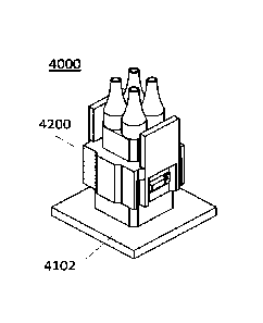
[0095] Fig. 14 shows a simplified cross-sectional view of parts of an assembly
1000 of
the second embodiment comprising a fiber optic connector 1200 and an electro-
optic
.. module 1100 in the form of a CBGA package mounted on a circuit board 1102,
wherein
the connector 1200 is inserted into the electro-optic module 1100 and latched
together
with latches 1204 engaging latch apertures 1122 in the metal sleeve 1208. As
illustrated
schematically, the faces of the optical fibers are positioned a predetermined
vertical
distance z from the optical aperture of the photonic device for effective
optical coupling.
.. Numbering of other components of the assembly is the same as Fig. 13.
[0096] Depending on how the array of semiconductor devices are mounted on the
substrate, the optical ports of the package are positioned to receive ferrules
of the optical
fibers with proper alignment in the lateral x-y direction and in the vertical
z direction. This
optical alignment will now be described in more detail.
.. [0097] By way of example only, Fig. 15 shows a photomicrograph of an
electro-photonic
chip 500 comprising a photodetector 502 and associate electronic circuitry 504
comprising a TIA amplifier with interconnect metallization to bond pads 506.
In this
particular chip, the photodetector and its optical aperture are near the
periphery of the
chip, while the electronic circuitry of the TIA amplifier occupies the central
area of the
chip. That is, the optical detector is not centered on the chip. Accordingly,
in assembly of
an electro-optical module containing an array of a plurality of chips of this
layout, the
chips are positioned on the substrate so that the array of optical ports for
the optical fibers
are aligned to the optical apertures of the photodetectors near the edge of
each chip.
Additional electronic circuitry may be provided on the chip, or other
electronic chips may
.. be mounted on the package substrate, e.g. comprising clock and data
recovery (CDR)
circuitry, to form a receive optical sub-assembly (ROSA).
[0098] Fig. 16 shows an enlarged and simplified schematic cross-sectional view
of part
of Fig. 14 to show x-y-z alignment of one fiber and one optical detector in an
assembly of
an electro-optical module and a fiber optic connector according to the second
embodiment, in which the photonic integrated circuit (chip) 500 comprises an
optical
detector having a layout similar to that shown in Fig. 15, comprising a photo-
diode 502
Date Recue/Date Received 2021-07-23
21
and adjacent electronic circuitry 504. The chip 500 is attached to the ceramic
substrate
1110 and electrically connected to conductive tracks 510 of the substrate by
wirebonds
512 extending from bond pads 506 of the chip 500. As an example, the optical
aperture
of the photo-diode detector 502 may be 20gm diameter. For example, the chips
may be
backside thinned, e.g. by chemical mechanical polishing, to a thickness of
e.g. 125gm
3 gm. The outside diameter of the optical fiber is typically 125 gm, and the
spot size of
the optical output from the optical fiber may be 10 gm at the fiber face, from
which the
optical beam diverges. The outside diameter of the ferrule 1126 of the optical
fiber
connector may be e.g. ¨1mm. To accommodate four fiber pigtails using standard
types
.. of commercially available connector components, the lateral dimensions of
the electro-
optical module may be, e.g. 9mm x 9mm or 7mm x 7mm. To account for lateral
tolerances, the mounting of the ferrule carrying the fiber within the fiber
optic connector
provides for some lateral play of a few microns, indicated as Ax-y,
represented
schematically by spring elements 1302 between the ferrule 1228 and the
connector body
1202. Similarly, to accommodate the thickness variation of the chip of e.g.
3 gm, the
mounting of the ferrule provides for a few microns of vertical play, indicated
by Az, and
represented by spring elements 1304. Additionally, to ensure that the fiber
end face does
not inadvertently contact the optical aperture of the photonic device, and
cause damage,
spacers 1306 are provided adjacent the chip 500. These spacers 1306 engage
alignment
surfaces of the ferrule surrounding the optical fiber and are sized to ensure
the optical
fiber is appropriately spaced vertically, in the z direction, to match the
beam spot size to
the optical aperture of the photo-diode. For example, automated machine vision
systems
are used to measure the actual distance to the chip surface and spacers of an
appropriate
thickness are provided, to form a stop to prevent the end of the fiber from
being inserted
too far, and to provide the appropriate vertical spacing to match the spot
size of the optical
beam for effective optical coupling to the aperture of the photo-diode.
[0099] For example, Fig. 17 shows a schematic view of an example of an electro-
photonic chip 500 mounted on a ceramic substrate 1110 with a spacer 1306 in
the form of
a calibrated dummy chip that acts as a spacer for z axis alignment. To account
for chip to
chip thickness variations, the thickness of the calibrated dummy chip 1306 is
selected
based on the finished thickness of chip 500.
Date Recue/Date Received 2021-07-23
22
[00100] Figs. 18 to 31 show a series of views of an assembly 2000 of an
electro-optic
module and a fiber optic connector of a third embodiment, and components
thereof. Many
features of this embodiment correspond to those of the first embodiment and
are labelled
with the same reference numerals incremented by 2000. As shown in Figs. 18, 19
and
20, the assembly comprises a surface mount electro-optic module 2100 and a
fiber optic
connector 2200. The module 2100 provides an array of four ferrule sockets 2128
on the
cap and a ball grid array 2114 on the underside. More details of the electro-
optic module
2100 are shown in Figs. 20 to 24, and more details of the fiber optic
connector 2200 are
shown in Figs. 25 to 29. For example, the details of the form of the body of
the module
.. 2100 and the connector 2200 differ and its components differ from the first
embodiment,
e.g. the connector provides latch opening 2210 and the module 2100 provides
latch
protrusions 2122. Fig. 29 shows more details of the internal components of the
male
optical fiber connector including the fiber optic ferrules 2226 and the spring
mechanism
comprising compression springs 2227. More detailed cross-sectional views of
the
components of the assembly are shown in Figs. 30 and 31. Fig. 30 shows a cross-
sectional
view of components comprising the electro-optical module and male optical
connector of
the third embodiment during assembly, showing internal components. Fig. 31
shows a
cross-sectional view of the same components after assembly.
[00101] In the first embodiment described above, the latch means comprises a
latch plate
.. which is a separate component. In variants of this assembly, the latch
elements are
integrated with the electro-optical module and/or the optical connector as
described above
for the other embodiments.
[00102] In the electro-optical assemblies of the embodiments illustrated and
described
above, the array of optical ports of the cap of the package comprises ferrule
sockets, and
the optical fiber connector is a male fiber connector carrying the plurality
of optical fiber
connectors which comprises a corresponding array optical fiber ferrules. In
alternative
embodiments, the array of optical ports of the CBGA package module comprises
an array
of ferrules comprising optical fiber stubs aligned to optical emitters or
receivers. Thus,
for example, the ferrule sockets on the CBGA package are replaced with stub
ferrules that
have fibers fused with glass solder to withstand oven temperatures. The fiber
stubs accept
split sleeves of a standard ferrule to ferrule attachment. For example, in an
embodiment,
Date Recue/Date Received 2021-07-23
23
the ferrule stubs are hard attached to the cap of the optical CBGA package,
and a high
temperature index matching epoxy is used to reduce Fresnel losses between the
fiber stub
and optical aperture of the photodiode. If appropriate, a lensed fiber could
also be
fashioned into the ferrule stub on the photodiode end.
[00103] Fig. 32 shows a simplified schematic lateral cross-sectional view of
components
of an assembly of an electro-optic module and a fiber optic connector of a
fourth
embodiment, during alignment and insertion of the fiber optic connector into
the electro-
optic module. Again, many components correspond to those of the first
embodiment, and
are labelled with the same reference numerals incremented by 3000. The male
optical
connector 3200 of this embodiment is the same as that of the second
embodiment. On the
other hand, the electro-optical module 3100 of this embodiment differs in
that, instead of
having an array of ferrule sockets, the module 3100 comprises an array of
ferrules of
optical fiber stubs 3126. The fiber optic ferrules of each of the fibers of
the fiber connector
3200 are connected to the fiber optic ferrules of the electro-optic module
using split
.. sleeves 3130.
[00104] Thus, for example, the ferrule sockets on the CBGA package are
replaced with
stub ferrules that have fibers fused with glass solder to withstand oven
temperatures. The
fiber stubs accept split sleeves of a standard ferrule to ferrule attachment.
For example,
in an embodiment, the ferrule stubs are hard attached to the cap of the CBGA
package,
and a high temperature index matching epoxy is used to reduce Fresnel losses
between
the fiber stub and optical aperture of the photodiode. If appropriate, a
lensed fiber could
also be fashioned into the ferrule stub on the photodiode end.
[00105] For example, Figs. 33 to 46 show a series of views of an assembly 4000
of an
electro-optic module 4100 and a fiber optic connector 4200 of a fifth
embodiment, and
components thereof. Many features of this embodiment correspond to those of
the first
embodiment and are labelled with the same reference numerals incremented by
4000. As
shown in Figs. 33 and 34 the assembly comprises a surface mount electro-optic
module
4100 and a fiber optic connector 2200. More details of the electro-optic
module 4100 are
shown in Figs. 35 to 39. The module 4100 provides a cap with an array of four
ferrules
4126, comprising fiber optic stubs on the top surface, and a ball grid array
4114 on the
underside. As shown in Fig. 39, an array of electro-optical chips 500 are
mounted on the
Date Recue/Date Received 2021-07-23
24
ceramic substrate 4110, and ferrules 4126 of fiber optic stubs are mounted
over the chips
with ferrule flanges 4127. More details of the fiber optic connector 4200 are
shown in
Fig. 40 to 44. Fig. 44 shows more details of the internal components of the
male optical
fiber connector including the fiber optic ferrules 4226 and the spring
mechanism
comprising compression springs 4227, sleeves 4229, gasket 4209. The connector
body
or housing 4202 is secured to the inner body or frame 4203 with fastener 4207.
Ferrules
4126 and 4226 of the surface mount module and of the fiber optic connector
are, for
example, 1.25mm chamfered ferrules. More detailed cross-sectional views of the
components of the assembly are shown in Figs. 45 and 46. Fig. 45 shows a cross-
sectional
view of components comprising the electro-optical module 4100 and male optical
connector 4200 of the third embodiment during assembly, showing internal
components,
numbered as in Figs. 33 to 44, and with the split sleeves 4130 in place over
the ferrules
4126 of the fiber stubs. Fig. 46 shows a cross-sectional view of the same
components
after assembly, with the latches securing the connector to the electro-optical
module, with
.. the ferrules 4226 inserted into the split sleeves 4130 for optical
coupling.
[00106] Surface mount electro-optic modules and fiber optic connectors of
various
embodiments are described above in which the optical fiber pigtails are
surface mounted
and vertically coupled to the electro-optical module through the optical
connector. These
embodiments are described by way of example only. Any specific dimensions of
.. components mentioned above are also provide by way of example only. For
future high-
density data centre interconnect, it may be desirable to further miniaturize
the electro-
optical module and optical fiber connectors packaging. It will be appreciated
that
modifications may be made to these embodiments, e.g., for packaging of
photonic
integrated circuits of different layouts, for packaging of arrays of different
numbers of
photonic chips. For example, embodiments are described for a quad package
arrangement
of a 2 x 2 array of photonic integrated circuits comprising optical transmit
or receive
devices. It will be appreciated that the disclosed packaging is scalable for
other numbers
of devices and detachable optical fiber connectors with a corresponding number
of optical
fiber pigtails. Some elements of the embodiments described may be combined in
different
ways to provide variants of these embodiments, e.g. comprising different forms
of latch
means and alignment means.
Date Recue/Date Received 2021-07-23
25
[00107] Other electro-photonic chips with surface emitting or receiving
devices may be
configured differently, with the optical aperture of the emitter or detector
centered or
placed in another position on the chip. Alternatively, in other
configurations, the optical
devices may be laterally (edge) coupled to ports at one side of the substrate,
e.g. for side
emitting laser diodes, and emitter chips comprising a laser diode in
combination with one
or more of a modulator, optical waveguide, and associated electronics.
[00108] Thus, in another configuration, the optical fiber pigtails may be edge
coupled to
the electro-optical module. An example of an assembly of an embodiment
comprising an
edge coupled electro-optical module and its corresponding optical connector is
described
below with reference to Figs. 47 to 52.
[00109] Fig. 47 shows an isometric schematic view of an electro-optical module
300 of
a third embodiment, in which the plurality of optical fibers are edge coupled
to a BGA
type package. That is, an array of four optical fiber ports comprising sockets
328 are
provided along one side of the ceramic BGA package, as illustrated in the
schematic side
view shown in Fig. 48, which shows the module 300 comprising the array of
optical fiber
sockets 328, when it is surface mounted on a substrate, such as a PCB 302,
with a latch
plate 310 comprising latch openings for receiving latches of an optical fiber
connector.
As described for the module of the first embodiment, the electro-optical
module 300 may
be surface mounted and directly attached to the underlying substrate by a
process
comprising pick-and-place and solder reflow. Fig. 49 shows a schematic plan
view of the
underside 312 of the electro-optical module of Fig. 49 showing the ball grid
array of ball
connections 314, and the array of optical fiber sockets 328.
[00110] Fig. 50 shows an isometric schematic view, and Fig. 51 shows a
schematic top
side view, of a male optical connector 400 for the electro-optical module 300
of the third
embodiment. Four optical fibers 420 and optical fiber connectors 428 are
inserted into the
body 402 of the connector. Fig. 52 shows a corresponding schematic end view of
the
male optical connector 400 of the third embodiment, with optical fibers and
optical fiber
connectors 428 inserted. In this embodiment, the latch means comprises a pair
of latch
elements 404 extending from the body 402 of the optical connector, which mate
with latch
engaging surfaces of the electro-optical module to enable the two parts to be
securely
latched together with the optical fibers aligned to the optical transceivers.
An assembly
Date Recue/Date Received 2021-07-23
26
comprising an electro-optical module and fiber optical connector of this
embodiment
provides for edge coupling (i.e. lateral or side coupling) of the optical
fiber pigtails to the
PCB on which the assembly is mounted. As for the assemblies with vertically
coupled
optical fiber pigtails, the electro-optical module 300 is similarly
fabricated, e.g. in the
form of a CBGA package, and surface mounted on the PCB by conventional pick-
and-
place and solder reflow processes. Latch means such as the latch arrangement
illustrated
allow the optical fiber connector to be detachably secured to the electro-
optical module.
It will be appreciated that this edge coupled connector geometry may be used
when the
electro-optical module comprises edge emitting optical device, or for
applications where
there is limited vertical spacing above the PCB to accommodate the fiber optic
pigtails.
As described for the vertically coupled connector geometry, if required, the
latch means
and alignment means for an edge coupled connector configuration comprise
components
comprising mating surfaces of the electro-optical module and the optical fiber
connector,
together with alignment means, such as spacers and spring components, which
provide
for alignment of the optical fibers with the optical apertures of an optical
emitter or optical
receiver of each electro-optical device, i.e. to provide precision alignment
in each of the
x, y and z directions for effective optical coupling of each optical fiber to
its respective
optical emitter or optical receiver. As for the embodiments of a vertically
coupled module,
in alternative embodiments of an edge coupled module, the ferrule sockets of
the electro-
2 0 .. optical module may be replaced with ferrule stubs, and split sleeves
are used to connect
the ferrules of the package module and the ferrules of the optical connector.
[00111] While specific embodiments of electro-optical modules, fiber optic
connectors,
and assemblies of electro-optical modules and fiber optic connectors have been
described
in detail, by way of example, it will be appreciated that elements of these
embodiments
may be combined in different ways to provide alternative embodiments, and
modifications may be made to these embodiments, e.g. for packaging of photonic
integrated circuits of different layouts, for packaging of arrays of different
numbers of
photonic chips, and fiber optic connectors carrying corresponding different
numbers of
optical fibers.
100112] Although embodiments of the invention have been described and
illustrated in
detail, it is to be clearly understood that the same is by way of illustration
and example
Date Recue/Date Received 2021-07-23
27
only and not to be taken by way of limitation, the scope of the present
invention being
limited only by the appended claims.
Date Recue/Date Received 2021-07-23