Note : Les descriptions sont présentées dans la langue officielle dans laquelle elles ont été soumises.
CA 03062469 2019-11-05
1
Saint-Gobain Glass France 2017423-WO
FF
Pane Having an Electrically Conductive Coating, with Reduced Visibility of
Fingerprints
The invention relates to a pane having an electrically conductive coating, as
well as
production and use thereof.
Glass panes with transparent electrically conductive coatings are known. The
glass
panes can thus be provided with a function without substantially disrupting
through-vision
through the pane. Such coatings are used, for example, as heatable coatings or
thermal
io radiation reflecting coatings on window panes for vehicles or buildings.
The interior of a motor vehicle or of a building can heat up greatly during
the summer
with high ambient temperatures and intense direct sunlight. In contrast, when
the outside
temperature is lower than the temperature in the interior, which occurs in
particular in the
winter, a cool pane acts as a heat sink, which is perceived as unpleasant.
Also, the
interior must be heated strongly in order to avoid cooling via the window
panes.
Thermal radiation reflecting coatings (so-called "low-E coatings") reflect a
significant part
of sunlight, in particular in the infrared range, which, in the summer,
results in reduced
warming of the interior. Moreover, the coating reduces the emission of
longwave thermal
radiation into the interior. With low outside temperatures in winter, it also
reduces the
outward emission of heat from the interior into the external surroundings.
For optimum effect, the thermal radiation reflecting coating must be arranged
on the
exposed interior-side surface of the pane, i.e., so to speak, between the
interior and the
actual glass pane. There, the coating is exposed to the atmosphere, ruling out
the use
of corrosion prone coatings based, for example, on silver. Due to their
corrosion
resistance and good conductivity, coatings based on transparent conductive
oxides
(TCO), for example, indium tin oxide (ITO) have proved themselves as
electrically
conductive coatings on exposed surfaces. Such coatings are known, for example,
from
EP 2 141 135A1, WO 2010115558 A1, and WO 2011105991 Al.
Coatings on exposed surfaces have the disadvantage that they can be touched by
individuals, possibly leaving fingerprints. The fingerprints are often
particularly readily
visible on the coatings, which can greatly reduce the aesthetic effect of the
pane or result
CA 03062469 2019-11-05
2
Saint-Gobain Glass France 2017423-WO
FF
in disturbing local changes in light reflection. Fingerprints are sometimes
difficult to
remove with customary cleaning agents, with the additional necessity of being
careful
not to damage the coating with chemicals or strong mechanical stress during
cleaning.
Known approaches for reducing the visibility of fingerprints include the use
of roughened
surfaces or hydrophobic and oleophobic layers as presented, for example, in
US2010304086A1, which can, however, make the production of the panes more
difficult
or limit their potential uses. U82003179455A1 discloses a two-layer
antireflection
coating for plastic parts that is supposed to reduce the visibility of
fingerprints. The layer
io .. thicknesses are selected such that they correspond to half or to one-
fourth the average
wavelength in order to achieve suitable interference effects.
US20130129945A1 discloses a pane with a thermal radiation reflecting coating,
for
example, constructed, starting from the substrate, from a silicon nitride
layer, a silicon
oxide layer, an ITO layer, another silicon nitride layer, another silicon
oxide layer, and a
final titanium oxide layer. The coating is applied on an external glass
surface and has
self-cleaning properties as a result of the titanium oxide final layer. The
visibility of
fingerprints is outside the scope of US20130129945A1.
US20150146286A1 discloses a pane with a thermal radiation reflecting coating,
constructed, starting from the substrate, from a silicon oxide layer, an ITO
layer, a silicon
nitride layer, and another silicon oxide layer. The coating is applied on the
interior-side
external glass surface. The visibility of fingerprints is outside the scope of
US20150146286A1.
US6416194B discloses a mirror, comprising a substrate and a reflecting
coating. The
reflectance spectrum of the coating has a local maximum at 428 nm. A local
minimum
shifted to shorter wavelengths is not disclosed, but seems, based on
extrapolation of the
reflectance spectrum, to be between 175 nm and 260 nm.
The object of the present invention is to provide a further improved pane
having an
electrically conductive coating on an exposed surface, on which fingerprints
are less
clearly visible.
CA 03062469 2019-11-05
3
Saint-Gobain Glass France 2017423-WO
FF
The object of the present invention is accomplished according to the invention
by a pane
having an electrically conductive coating in accordance with claim 1.
Preferred
embodiments are evident from the dependent claims.
The pane according to the invention comprises a substrate and an electrically
conductive
coating on an exposed surface of the substrate. The coating according to the
invention
includes at least one electrically conductive layer. In the context of the
invention, the term
"exposed surface" means a surface of the substrate that is accessible and has
direct
contact with the surrounding atmosphere such that the coating can be directly
touched
io by an individual or, for example, can be contaminated by dirt, oils, or
fats. The coating is
sufficiently corrosion resistant to be used on an exposed surface.
Fingerprints consist of a mixture of different biological substances, in
particular, fats and
acids. According to values in the literature, a refractive index of approx.
1.3 to 1.6 can
be assumed for fingerprints. The inventors found through measurements by white
light
interference microscopy (WLIM) that typical fingerprints have a thickness of a
few
nanometers up to several hundred nanometers. The invention is based on the
knowledge
that the visibility of fingerprints up to a thickness of a few hundred
nanometers can be
influenced by interference optics, which can in turn be adjusted through the
design of the
layer system forming the coating. Very thick fingerprints can, to be sure, be
less
influenced by interference optics; however, the overall optics of the pane are
substantially improved if at least the fingerprints with a thickness of a few
hundred
nanometers, which make up the majority of all fingerprints, are less visible.
The inventors
surprisingly realized that a pane having an electrically conductive coating
that is set such
that it has a local minimum of reflectance in the range from 310 nm to 360 nm
and a local
maximum of reflectance in the range from 400 nm to 460 nm results in reduced
visibility
of typical fingerprints. The local minimum of reflectance is preferably in the
range from
315 nm to 355 nm, particularly preferably from 320 nm to 350 nm. The local
maximum
of reflectance is preferably in the range from 415 nm to 450 nm. Said local
extreme
values are to be understood as as a minimum requirement and are not intended
to rule
out the fact that these are global extreme values. While in the case of the
maximum of
reflectance, at least outside the visible range, spectral ranges exist that
have higher
reflectance, it is also, however, conceivable that said local minimum of
reflectance is the
globale minimum in the mathematical sense.
CA 03062469 2019-11-05
4
Saint-Gobain Glass France 2017423-WO
FF
The term "reflectance" is used as defined in the DIN EN 410 standard.
"Reflectance"
always refers to the layer-side reflectance that is measured when the coated
surface of
the pane faces the light source and the detector. The values indicated for
refractive
indices are measured at a wavelength of 550 nm.
The coating according to the invention is, in a preferred embodiment, a
thermal radiation
reflecting coating. Such a coating is often also referred to as low-E coating,
low emissivity
coating, or emissivity reducing coating. Its function is to prevent
irradiation of heat into
the interior (IR portions of sunlight and, in particular, the thermal
radiation of the pane
o itself) and also the emission of heat out of the interior. However, the
coating can, in
principle, also fulfill other functions when it is electrically contacted such
that it is heated
as a result of an electric current flow.
The pane according to the invention is preferably a window pane and is
intended, in an
opening, for example, of a vehicle or a building, to separate the interior
from the external
environment. The exposed surface on which the coating according to the
invention is
arranged is preferably the interior-side surface of the pane or of the
substrate. In the
context of the invention, the term "interior-side surface" means that surface
that is
intended to face the interior in the installed position of the pane. This is
particularly
advantageous in terms of the thermal comfort in the interior. With high
outdoor
temperatures and sunlight, the coating according to the invention can
particularly
effectively at least partially reflect the thermal radiation radiated by the
entire pane in the
direction of the interior. With low outdoor temperatures, the coating
according to the
invention can effectively reflect the thermal radiation emitted from the
interior and thus
reduce the effect of the cold pane as a heat sink. Customarily, the surfaces
of a glazing
are numbered from the outside to the inside such that the interior-side
surface is referred
to as "side 2" in the case of a single glazing, as "side 4" in the case of a
double glazing
(for example, laminated glass or insulating glazing units). However, the
coating can,
alternatively, also be arranged on the outside surface of the pane. It can be
useful, in
particular in the architectural sector, for example, as an anti-condensation
coating on a
window pane.
However, alternatively, the coating can also fulfill other functions, for
example, as an
electrically based capacitive or resistive sensor for tactile applications,
such as touch
screens or touch panels, which are naturally often soiled by fingerprints.
CA 03062469 2019-11-05
Saint-Gobain Glass France 2017423-WO
FF
The coating is a sequence of thin layers (layer structure, layer stack).
Whereas the
electrical conductivity is ensured by the at least one electrically conductive
layer, the
optical properties, in particular transmittance and reflectivity, are
significantly influenced
5 by the other layers and can be selectively set by their design. So-called
"antireflection
layers", which have a lower refractive index than the electrically conductive
layer and are
arranged above and below it, have a special influence in this context. In
particular as a
result of interference effects, these antireflection layers can increase
transmittance
through the pane and reduce reflectivity. The effect is, decisively, a
function of refractive
.. index and layer thickness. In an advantageous embodiment, the coating
includes in each
case at least one antireflection layer below and above the electrically
conductive layer,
with the antireflection layers having a lower refractive index than the
electrically
conductive layer, preferably a refractive index of at most 1.8, in particular
of at most 1.6.
The coating according to the invention is transparent, thus does not
appreciably restrict
through-vision through the pane. The absorption of the coating is preferably
from approx.
1% to approx. 20% in the visible spectral range. The term "visible spectral
range" means
the spectral range from 380 nm to 780 nm.
In the context of the invention, if a first layer is arranged "above" a second
layer, this
means that the first layer is farther from the substrate than the second layer
is. In the
context of the invention, if a first layer is arranged "below" a second layer,
this means
that the second layer is farther from the substrate than the first layer is.
In the context of
the invention, if a first layer is arranged above or below a second layer,
this does not
.. necessarily mean that the first and the second layer are in direct contact
with one
another. One or more additional layers can be arranged between the first and
the second
layer, unless this is explicitly ruled out.
The coating is typically applied full-surface on the substrate surface,
possibly with the
exception of a circumferential edge region and/or other locally limited
regions that can
serve, for example, for data transmission. The coated portion of the substrate
surface is
preferably at least 90%.
In the context of the invention, if a layer or other element "contains" at
least one material,
this includes the case that the layer is made of the material, which is, in
principle, also
CA 03062469 2019-11-05
6
Saint-Gobain Glass France 2017423-WO
FF
preferable. The compounds described within the present invention, in
particular oxides,
nitrides, and carbides can, in principle, be stoichiometric,
substoichiometric, or
superstoichiometric, even though, for the sake of better understanding, the
stoichiometric molecular formulae are cited.
For the reduced visibility of fingerprints or surface contamination, the
occurrence
according to the invention of the local extrema of reflectance is crucial.
These properties
can, in principle, be realized by a large number of embodiments of the layer
structure of
the coating, and the invention should not be limited to a specific layer
structure. In
lo principle, the extreme value distribution is determined by the selection
of the layer
sequence, the materials of the individual layers, and the respective layer
thicknesses,
wherein it can be influenced by a temperature treatment occurring after the
coating.
However, certain embodiments that are presented in the following have also
proved to
be particularly advantageous in terms of optimized material use and other
optical
properties.
The electrically conductive layer preferably has a refractive index of 1.7 to
2.3. In an
advantageous embodiment, the electrically conductive layer contains at least
one
transparent, electrically conductive oxide (TCO, transparent conductive
oxide). Such
layers are corrosion resistant and can be used on exposed surfaces. The
electrically
conductive layer preferably contains indium tin oxide (ITO), which has proved
itself
particularly well, in particular due to low specific resistance and low
scattering in terms
of sheet resistance. However, the conductive layer can, alternatively, also
contain, for
example, mixed indium zinc oxide (IZO), gallium-doped tin oxide (GTO),
fluorine-doped
tin oxide (Sn02:F), or antimony-doped tin oxide (Sn02:Sb).
The thickness of the electrically conductive layer is preferably from 50 nm to
130 nm,
particularly preferably from 60 nm to 100 nm, for example, from 65 nm to 80
nm. With
this, particularly good results are achieved in terms of electrical
conductivity with
sufficient optical transparency at the same time.
In an advantageous embodiment, the coating includes a dielectric lower
antireflection
layer that is arranged below the electrically conductive layer. The refractive
index of the
lower antireflection layer is preferably at most 1.8, particularly preferably
from 1.3 to 1.8.
CA 03062469 2019-11-05
7
Saint-Gobain Glass France 2017423-WO
FF
The thickness of the lower antireflection layer is preferably from 5 nm to 50
nm, more
preferably from 10 nm to 30 nm, for example, from 10 nm to 20 nm.
In an advantageous embodiment, the coating includes a dielectric upper
antireflection
layer that is arranged above the electrically conductive layer. The refractive
index of the
upper antireflection layer is preferably at most 1.8, particularly preferably
from 1.3 to 1.8.
The thickness of the upper antireflection layer is preferably from 10 nm to
100 nm,
particularly preferably from 30 nm to 70 nm, for example, from 45 nm to 55 nm.
io In a particularly advantageous embodiment, the coating has both a lower
antireflection
layer below the electrically conductive layer and an upper antireflection
layer above the
electrically conductive layer.
The antireflection layers bring about, in particular, advantageous optical
properties of the
pane. They reduce the reflectance and thus increase the transparency of the
pane and
ensure a neutral color impression. The antireflection layers preferably
contain an oxide
or fluoride, particularly preferably silicon oxide, aluminum oxide, magnesium
fluoride, or
calcium fluoride. The silicon oxide can be doped and is preferably doped with
aluminum
(S102:A1), with boron (Si02:B), with titanium (Si02:Ti), or with zirconium
(Si02:Zr).
However, the layers can, alternatively, also contain, for example, aluminum
oxide
(A1203).
In a particularly advantageous embodiment, the upper antireflection layer is
the
uppermost layer of the coating. It thus has the greatest distance from the
substrate
surface and is the final layer of the layer stack, which is exposed and also
accessible
and touchable by individuals. In this case, the optical properties of the
layer stack are
optimal in terms of reduced visibility of fingerprints. Additional layers
above the
antireflection layer, in particular with a higher refractive index than the
antireflection layer,
would change the optical properties and could reduce the desired effect.
It has been shown that the oxygen content of the electrically conductive
layer, in
particular when this is based on a TOO, has a significant influence on its
properties, in
particular on transparency and conductivity. The production of the pane
typically includes
a temperature treatment, for example, a thermal tempering process, wherein
oxygen can
diffuse to the conductive layer and oxidize it. In an advantageous embodiment,
the
CA 03062469 2019-11-05
8
Saint-Gobain Glass France 2017423-WO
FF
coating between the electrically conductive layer and the upper antireflection
layer
includes a dielectric barrier layer for regulating oxygen diffusion having a
refractive index
of at least 1.9. The barrier layer serves to adjust the supply of oxygen to an
optimum
level. Particularly good results are obtained when the refractive index of the
barrier layer
is from 1.9 to 2.5.
The dielectric barrier layer for regulating oxygen diffusion contains at least
a metal, a
nitride, or a carbide. The barrier layer can contain, for example, titanium,
chromium,
nickel, zirconium, hafnium, niobium, tantalum, or tungsten or a nitride or
carbide of
io tungsten, niobium, tantalum, zirconium, hafnium, chromium, titanium,
silicon or
aluminum. In a preferred embodiment, the barrier layer contains silicon
nitride (Si3N4) or
silicon carbide, in particular silicon nitride (Si3N4), with which
particularly good results are
obtained. The silicon nitride can be doped and is, in a preferred further
development,
doped with aluminum (Si3N4:A1), with zirconium (Si3N4:Zr), with titanium
(Si3N4:Ti), or with
boron (Si31\14:6). In a temperature treatment after application of the coating
according to
the invention, the silicon nitride can be partially oxidized. Then, after the
temperature
treatment, a barrier layer deposited as Si3N4 contains SixNyOz, wherein the
oxygen
content is typically from 0 atom-% to 35 atom-%.
The thickness of the barrier layer is preferably from 5 nm to 20 nm,
particularly preferably
from 7 nm to 12 nm, for example, from 8 nm to 10 nm. Thus, the oxygen content
of the
conductive layer is particularly advantageously regulated. The thickness of
the barrier
layer is selected with regard to oxygen diffusion, less with regard to optical
properties of
the pane. However, it has been shown that barrier layers with thicknesses in
the range
indicated are compatible with the coating according to the invention and its
optical
requirements.
In an advantageous embodiment, the coating includes, below the electrically
conductive
layer, and, optionally, below the lower antireflection layer, a dielectric
blocking layer
against alkali diffusion. The blocking layer reduces or prevents the diffusion
of alkali ions
out of the glass substrate into the layer system. Alkali ions can adversely
affect the
properties of the coating. Furthermore, the blocking layer, in interaction
with the lower
antireflection layer, contributes advantageously to the setting of the optics
of the coating
structure as a whole. The refractive index of the blocking layer is preferably
at least 1.9.
Particularly good results are obtained when the refractive index of the
blocking layer is
CA 03062469 2019-11-05
9
Saint-Gobain Glass France 2017423-WO
FF
from 1.9 to 2.5. The blocking layer preferably contains an oxide, a nitride,
or a carbide,
preferably of tungsten, chromium, niobium, tantalum, zirconium, hafnium,
titanium,
silicon, or aluminum, for example, oxides such as W03, Nb2O5, Bi203, TiO2,
Ta205, Y203,
ZrO2, Hf02 Sn02, or ZnSnOx, or nitrides such as AIN, TiN, TaN, ZrN, or NbN.
The
blocking layer particularly preferably contains silicon nitride (Si3N4), with
which
particularly good results are obtained. The silicon nitride can be doped and
is, in a
preferred further development, doped with aluminum (Si3N4:A1), with titanium
(Si3N4:Ti),
with zirconium (Si3N4:Zr), or with boron (Si3N4:B). The thickness of the
blocking layer is
preferably from 10 nm to 50 nm, particularly preferably from 20 nm to 40 nm,
for example,
io from 25 nm to 35 nm. The blocking layer is preferably the bottommost
layer of the layer
stack, i.e., has direct contact with the substrate surface, where it can have
optimum
effect.
The coating consists, in an advantageous embodiment, exclusively of layers
having a
is refractive index of at least 1.9 or of at most 1.8, preferably at most
1.6. In a particularly
preferred embodiment, the coating consists only of the layers described and
contains no
further layers. The coating then consists of the following layers in the order
indicated,
starting from the substrate surface:
- blocking layer against alkali diffusion
20 -lower antireflection layer
- electrically conductive layer
- barrier layer for regulating oxygen diffusion
- upper antireflection layer.
25 The interior-side emissivity of the pane according to the invention is
preferably less than
or equal to 45%, particularly preferably less than or equal to 35%, most
particularly
preferably less than or equal to 30%. Here, the term "interior-side
emissivity" refers to
the measurement that indicates how much thermal radiation the pane gives off
in the
installed position compared to an ideal thermal radiator (a black body) in an
interior, for
30 example, of a building or of a vehicle. In the context of the invention,
"emissivity" means
the total normal emissivity at 283 K per the standard EN 12898.
The sheet resistance of the coating according to the invention is preferably
from 10
ohm/square to 100 ohm/square, particularly preferably from 15 ohm/square to 35
35 ohm/square.
=
CA 03062469 2019-11-05
Saint-Gobain Glass France 2017423-WO
FF
The substrate is made of an electrically insulating, in particular a rigid
material, preferably
of glass or plastic. The substrate contains, in a preferred embodiment, soda
lime glass,
but can, in principle, also contain other types of glass, for example,
borosilicate glass, or
5 quartz glass. The substrate contains, in another preferred embodiment,
polycarbonate
(PC) or polymethyl methacrylate (PMMA). The substrate can be as transparent as
possible or also tinted or colored. The substrate preferably has a thickness
of 0.1 mm to
mm, typically of 2 mm to 5 mm. The substrate can be flat or curved. In a
particularly
advantageous embodiment, the substrate is a thermally tempered glass pane.
The invention also includes a method for producing a pane having an
electrically
conductive coating, wherein
(a) an electrically conductive coating that comprises at least one
electrically conductive
layer is applied on an exposed surface of a substrate; and
(b) the substrate with the coating is subjected to a temperature treatment at
at least
100 C, whereafter the pane has a local minimum of reflectance in the range
from
310 nm to 360 nm, in particular 320 nm to 350 nm and a local maximum of
reflectance
in the range from 400 nm to 460 nm.
The pane is subjected, after application of the heatable coating to a
temperature
treatment, which, in particular, improves the crystallinity of the functional
layer. The
temperature treatment is preferably done at at least 300 C. In particular,
the temperature
treatment reduces the sheet resistance of the coating. Moreover, the optical
properties
of the pane are significantly improved, in particular transmittance is
increased.
The temperature treatment can be done in various ways, for example, by heating
the
pane using a furnace or a radiant heater. Alternatively, the temperature
treatment can
also be done by irradiation with light, for example, with a lamp or a laser as
the light
source.
In an advantageous embodiment, the temperature treatment is done, in the case
of a
glass substrate, within a thermal tempering process. The heated substrate is
subjected
to a stream of air, rapidly cooling the substrate. Compressive stresses
develop at the
surface of the pane and tensile stresses develop in the core of the pane. The
CA 03062469 2019-11-05
11
Saint-Gobain Glass France 2017423-WO
FF
characteristic distribution of stresses increases the breaking strength of the
glass panes.
A bending process can also precede the tempering.
The individual layers of the heatable coating are deposited by methods known
per se,
preferably by magnetron-enhanced cathodic sputtering. This is particularly
advantageous in terms of a simple, quick, economical, and uniform coating of
the
substrate. The cathodic sputtering is done in a protective gas atmosphere, for
example,
of argon, or in a reactive gas atmosphere, for example, by addition of oxygen
or nitrogen.
The layers can, however, also be applied using other methods known to the
person
skilled in the art, for example, by vapor deposition or chemical vapour
deposition (CVD),
by atomic layer deposition (ALD), by plasma-enhanced chemical vapor deposition
(PECVD), or using wet chemical methods.
In an advantageous embodiment, a blocking layer against alkali diffusion is
applied
before the electrically conductive layer. In an advantageous embodiment, a
lower
reflection layer is applied before the electrically conductive layer and,
optionally, after the
blocking layer. In an advantageous embodiment, a barrier layer for regulating
oxygen
diffusion is applied after the conductive layer. In an advantageous
embodiment, an upper
antireflection layer is applied after the conductive layer and, optionally,
after the barrier
layer.
For the selection of suitable materials and layer thicknesses to realize the
reflection
spectrum according to the invention, the person skilled in the art can, for
example, use
simulations customary in the art.
The invention also includes the use of a pane according to the invention in
buildings, in
electrical or electronic equipment, or in means of transportation for travel
on land, in the
air, or on water. The pane is preferably used as a window pane, for example,
as a
building window pane or as a roof panel, side window, rear window, or
windshield of a
vehicle, in particular of a motor vehicle. Alternatively, the pane is
preferred as an
electrically based capacitive or resistive sensor for tactile applications,
for example, as a
touch screen or a touch panel.
CA 03062469 2019-11-05
12
Saint-Gobain Glass France 2017423-WO
FF
In the following, the invention is explained in detail with reference to
drawings and
exemplary embodiments. The drawings are a schematic representation and are not
to
scale. The drawings in no way restrict the invention.
They depict:
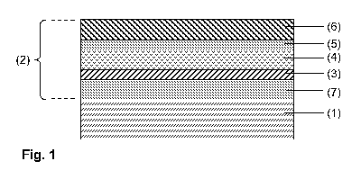
Fig. 1 a cross-section through an embodiment of the pane according to the
invention
having a heatable coating,
Fig. 2 a flowchart of an embodiment of the method according to the invention,
Fig. 3 a diagram of reflectance RL as a function of wavelength for two
examples
io according to the invention and two comparative examples, and
Fig. 4 simulation results of the relative reflectance as a function of the
thickness of an
oil film deposited on the on the coating 2 for the examples and comparative
examples of Fig. 3.
Fig. 1 depicts a cross-section through an embodiment of the pane according to
the
invention with the substrate 1 and the electrically conductive coating 2. The
substrate 1
is, for example, a glass pane made of tinted soda lime glass and has a
thickness of
2.1 mm. The coating 2 is a thermal radiation reflecting coating (low-E
coating). The pane
is intended, for example, as a roof panel of a motor vehicle. Roof panels are
typically
implemented as composite glass panes, wherein the substrate 1 is joined by its
surface
facing away from the coating 2 to an outer pane (not shown) via a
thermoplastic film.
The substrate 1 forms the inner pane of the composite glass, wherein the
coating 2 is
applied on the exposed interior-side surface that can be touched directly by
the vehicle
occupants. As a result, fingerprints can accumulate on the coating 2. The
optical
properties of the coating 2 are optimized such that fingerprints are less
highly visible than
with conventional coatings. This is accomplished according to the invention in
that the
coating is designed such that the pane has a local minimum of reflectance RL
in the
range from 320 nm to 350 nm and a local maximum of reflectance RL in the range
from
400 nm to 460 nm. Surprisingly, fingerprints are less noticeable under this
condition.
The coating 2 is a sequence of thin layers, comprising, starting from the
substrate 1, the
following individual layers: a blocking layer 7 against alkali diffusion, a
lower antireflection
layer 3, an electrically conductive layer 4, a barrier layer 5 for regulating
the oxygen
diffusion layer 5, and an upper antireflection layer 6. The materials and
layer thicknesses
CA 03062469 2019-11-05
13
Saint-Gobain Glass France
2017423-WO
FF
are summarized in Table 1. The individual layers of the coating 2 were
deposited by
magnetron-enhanced cathodic sputtering.
Table 1
Layer Reference No. Material
Thickness
Upper antireflection layer 6 Si02:Al 50 nm
Barrier layer 5 Si3N14:Al 9 nm
Electrically conductive layer 4 2 ITO 70 nm
Lower antireflection layer 3 Si02:Al 17 nm
Blocking layer 7 30 nm
Substrate 1 Soda lime glass 2.1
mm
Fig. 2 shows a flowchart of an exemplary embodiment of the production method
according to the invention.
io Fig. 3 shows diagrams of the reflectance ft. for four examples according
to the invention
and three comparative examples. The materials and layer thicknesses of the
coating 2
of examples 1-4 are summarized in Table 2; those of the comparative examples 1-
3, in
Table 3. In the examples 1-4, the pane comprised a substrate 1 of tinted soda
lime glass
with light transmittance TL of approx. 25% and the coating 2, which, starting
from the
substrate 1, was constructed from a blocking layer 7, a lower antireflection
layer 3, an
electrically conductive layer 4, a barrier layer 5, and an upper
antireflection layer 6. The
layers were formed from the same materials, with the coatings 2 of the
examples 1-4
differing in the layer thicknesses. However, for the examples 1-4 according to
the
invention, the coating 2 was, in contrast to the comparative examples, in each
case
adjusted such that the pane had a local minimum of reflectance RL in the range
from
320 nm to 350 nm and a local maximum of reflectance RL in the range from 400
nm to
460 nm, as can be seen in the figure. All panes had been subjected to a
temperature
treatment at approx. 650 C within a glass bending process.
Table 2
Thickness
Layer Material
Example 1 Example 2 Example 3 Example 4
6 SiO2 50 nm 55 nm 50 nm 50 nm
CA 03062469 2019-11-05
14
Saint-Gobain Glass France 2017423-WO
FF
Si3N4 9 nm 9 nm 9 nm 9 nm
4 ITO 70 nm 80 nm 70 nm 120 nm
3 SiO2 17 nm 10 nm 30 nm 15 nm
7 Si3N14 30 nm 25 nm 20 nm 10 nm
1 Glass 2.1 mm 2.1 mm 2.1 mm 2.1 mm
Table 3
Thickness
Layer Material
Comp. Ex, 1 Comp. Ex, 2 Comp. Ex, 3
TiO2 5 nm
6 SiO2 70 nm 70 nm 50 nm
5 Si31\14 9 nm 9 nm 9 nm
4 ITO 70 nm 80 nm 70 nm
3 Si02 30 nm 30 nm 17 nm
7 Si3N14 30 nm
1 Glass 2.1 mm 2.1 mm 2.1 mm
5
The comparative examples 1 and 2 basically differed from the examples
according to
the invention through the absence of the blocking layer 7, resulting in
significant changes
in the reflection spectrum, such that the local extrema did not occur
according to the
io invention. In the comparative example 3, yet another layer TiO2 was
applied above the
upper antireflection layer 6, as it is used, for example, as a photocatalytic
layer in self-
cleaning coatings. The upper antireflection layer 6 was, consequently, not the
uppermost
layer of the coating 2.
In contrast to the examples 1-4 according to the invention, the local extrema
of the
reflectance RL with the comparative examples 1-3 were not positioned in the
spectrum
according to the invention. The occurrence of the local extrema is summarized
in
Table 4. The values of reflectance RL presented were determined through
simulations
using CODE software.
CA 03062469 2019-11-05
Saint-Gobain Glass France 2017423-WO
FF
Table 4
Minimum RL Maximum RL
Ex. 1 335 nm 420 nm
Ex. 2 335 nm 425 nm
Ex. 3 345 nm 450 nm
Ex. 4 335 nm 450 nm
Comp. Ex. 1 <300 nm 350 nm
Comp. Ex. 2 305 nm 370 nm
Comp. Ex. 3 375 nm 425 nm
To take into account the influence of a fingerprint, the simulations were
expanded by an
oil film (refractive index 1.58) on the coating 2. The relative reflectance
for the examples
5 and comparative examples was then calculated as a quotient (reflectance
of the pane
with oil film) / (reflectance of the pane without oil film). The result is
presented in Fig. 4
as a function of the thickness of the oil film.
In the examples 1 and 2 according to the invention, the relative reflectance
for thin oil
10 films up to approx. 20 nm is approx. 1; i.e., the reflectance is hardly
changed by the oil
film. With thicker oil films, the reflectance increases slowly to a value of
approx. 2.5 with
an oil film of 100 nm. In the examples 3 and 4, the relative reflectance
decreases slightly
at the beginning and increases just as slowly starting at approx. 30 nm oil
film thickness.
15 In the comparative examples 1 and 2, a significantly different behavior
is seen. Already
with thin oil films, the reflection changes significantly and the relative
reflectance initially
decreases sharply. It then also increases starting at an oil film thickness of
approx.
nm, but significantly more sharply than in the examples according to the
invention. In
the case of comparative example 3, a much sharper increase of the relative
reflectance
20 can already be seen with very thin oil films.
From the examples and comparative examples, it can clearly be seen that the
presence
of an oil film results, in the case of the coatings 2 according to the
invention, in a
significantly less pronounced change in the reflectance than in the case of
coatings not
according to the invention. Fingerprints, which are essentially fat deposits
and are
CA 03062469 2019-11-05
16
Saint-Gobain Glass France 2017423-WO
FF
optically quite similar to an oil film, are thus significantly less visible
due to the lower
contrast. The fact that the visibility of fingerprints can be reduced by
simply optimizing
the optical properties of the coating was unexpected and surprising for the
person skilled
in the art.
Additional examples according to the invention (Ex. 6-12) and comparative
examples
(Comp. Ex. 4-12) are presented in Table 5. In each case, the thicknesses of
the individual
layers are indicated, from left to right starting from the substrate 1 (tinted
soda lime
glass). The spectral position of the local extrema of the reflectance RL is
summarized in
io Table 6. All panes were again subjected to a temperature treatment at
approx. 650 C in
a glass bending process.
Table 5
Layer 1 7 3 4 5 6
Material Glass Si3N4 SiO2 ITO Si31\14 SiO2 TiO2
Ex. 6 2.1 mm 30 nm 30 nm 75 nm 9 nm 30 nm -
Ex. 7 2.1 mm 40 nm 10 nm 70 nm 9 nm 50 nm -
Ex. 8 2.1 mm 15 nm 20 nm 90 nm 9 nm 50 nm -
Ex. 9 2.1 mm 20 nm 15 nm 100 nm 9 nm 45 nm -
Ex. 10 2.1 mm 25 nm 20 nm 60 nm 9 nm 50 nm -
Ex. 11 2.1 mm 25 nm 25 nm 50 nm 9 nm 60 nm -
Ex. 12 2.1 mm 20 nm 10 nm 70 nm 9 nm 70 nm -
Comp. Ex. 4 2.1 mm 20 nm 10 nm 70 nm 9 nm 70 nm 5 nm
Comp. Ex. 5 2.1 mm - 30 nm 70 nm 9 nm 50 nm -
Comp. Ex. 6 2.1 mm 0 nm 30 nm 70 nm 9 nm 50 nm 5 nm
Comp. Ex. 7 2.1 mm 20 nm 15 nm 100 nm 9 nm 45 nm 5 nm
Comp. Ex. 8 2.1 mm - 30 nm 100 nm 9 nm 55 nm -
Comp. Ex. 9 2.1 mm 10 nm 15 nm 120 nm 9 nm 50 nm 5 nm
Comp. Ex. 10 2.1 mm - 30 nm 120 nm 9 nm 75 nm -
Comp. Ex. 11 2.1 mm 25 nm 20 nm 60 nm 9 nm 50 nm 5 nm
Comp. Ex. 12 2.1 mm - 30 nm 50 nm 9 nm 50 nm -
Table 6
CA 03062469 2019-11-05
17
Saint-Gobain Glass France 2017423-WO
FF
Minimum RL Maximum RL
Ex. 6 330 nm 425 nm
Ex. 7 330 nm 415 nm
Ex. 8 340 nm 450 nm
Ex. 9 345 nm 455 nm
Ex. 10 320 nm 400 nm
Ex. 11 345 nm 410 nm
Ex. 12 355 nm 430 nm
Comp. Ex. 4 385 nm 455 nm
Comp. Ex. 5 385 nm 610 nm
Comp. Ex. 6 300 nm 370 nm
Comp. Ex. 7 385 nm 500 nm
Comp. Ex. 8 310 nm 375 nm
Comp. Ex. 9 390 nm 490 nm
Comp. Ex. 10 380 nm 460 nm
Comp. Ex. 11 365 nm 455 nm
Comp. Ex. 12 350 nm 560 nm
In reality, fingerprints have a wide range of thicknesses, including even
those with layer
thicknesses greater than 1 pm. In the case of such thick deposits, the effects
of
interference optics no longer play a decisive role such that visibility can no
longer be
significantly influenced by the optical properties of the coating 2. However,
for the
majority of fingerprints in the range up to approx. 100 nanometers, visibility
can be
significantly reduced. This significantly improves the overall impression of
the pane.
CA 03062469 2019-11-05
18
Saint-Gobain Glass France
2017423-WO
FF
List of Reference Characters:
(1) substrate
(2) heatable coating
(3) lower antireflection layer
(4) electrically conductive layer
(5) barrier layer for regulating oxygen diffusion
(6) upper antireflection layer
(7) blocking layer against alkali diffusion
RL reflectance (per DIN EN410)