Note : Les descriptions sont présentées dans la langue officielle dans laquelle elles ont été soumises.
CA 03063351 2019-11-12
WO 2018/234954
PCT/IB2018/054393
IMPROVED POWER SUPPLY HAVING FOUR QUADRANT CONVERTER AND
TECHNIQUES FOR OPERATION
CROSS-REFERENCE TO RELATED APPLICATIONS
[0001] The present international application claims priority to US Non-
Provisional Patent
Application No. 15/626,274 filed on June 19, 2017, the entire disclosure of
which is
incorporated herein by reference.
TECHNICAL FIELD
[0002] The present embodiments are related to general switched mode power
supplies
originated as for welding type power, that is, power generally used for
welding, cutting, or
heating, but applicable above and beyond.
BACKGROUND
[0003] A power supply (PS), in particular a switched mode power supply (SMPS)
converts
electric energy taken from a primary source of electrical power to electrical
energy having
parameters different than parameters of energy from the primary source. In
particular, a PS
intended for welding purposes may deliver electric power of direct current
(DC) and alternate
current (AC). The latter type of PS is often used for submerged arc welding
(SAW) and gas
tungsten arc welding (GTAW), better known as tungsten inert gas (TIG) welding.
Welding
processes conducted with alternating current have many challenges, but due to
technological
1
CA 03063351 2019-11-12
WO 2018/234954 PCT/IB2018/054393
difficulties in welding of certain metals and alloys as well as welding of
elements of certain
geometrical form and position, AC welding may be an appropriate choice.
[0004] There are a number of disadvantages, special requirements and
conditions related to
AC welding. In AC welding, the polarity of the voltage and direction of the
current are
periodically changing, such as at a rate of 10 Hz to 1000 Hz, merely as an
example. This
periodic change means that at certain points in time the current crosses a
zero value, resulting
in a condition where there is no electric arc and the output circuit is open.
During a zero
crossing event, the change of voltage polarity precedes the change of current
direction. The
explanation for this relationship lies in the presence of an inductance in the
output circuit.
After the change of voltage polarity, first the electric arc or conductive
path must be restored.
Once conduction is restored, the current rises up, with a rate dependent on
voltage capacity and
a sum of inductances in the output circuit. In AC power supplies using
sinusoidal AC current,
the voltage changes in a sinusoidal way at low frequencies. Usually the change
is not fast
enough to ignite arc plasma particles present in the electric arc, which
particles disappear
rapidly from the space between weld electrodes. In this circumstance, just a
high voltage can
ignite arc again. Usually, in an AC welding power supply with sinusoidal
output, an ignition
unit is used to generate a high voltage surge during every change of the
polarity, which
circumstance is undesirable for several reasons. In particular, the ignition
unit may be a high
voltage, high frequency generator, which unit produces copious amounts of
electromagnetic
interference of very high frequency. An alternative way of arc ignition is to
establish voltage
of the opposite polarity and increase current of the opposite direction as
fast as is possible.
Regarding the last requirement, the current at least should undergo direction
reversal in a range
of current near the zero point, large enough to sustain the electric arc as
long as possible, then
2
CA 03063351 2019-11-12
WO 2018/234954 PCT/IB2018/054393
sustain the arc after ignition with reverse polarity. The limitation of a fast
current transition to
the initial range arises from a trade-off between process stability and the
limitation of the
contents of high frequency harmonics of the current. In particular, high
frequency harmonics
of the welding current invokes effects including: a) high levels of acoustic
noise, b) high levels
of high frequency magnetic field around the power cables, and c) high
frequency losses in the
power cables. In any case, a solution for AC current welding is useful if
providing rapid
changes of the output voltage and the output current.
[0005] Another challenge in AC welding is the ignition of an arc after change
of polarity.
Even under conditions of rapid voltage change, the voltage level may not be
sufficient to ignite
the arc after polarity change. Therefore, power supplies that can deliver
increased voltage are
desirable. This feature also addresses the demand for high rate of the current
change. Notably,
TIG welding power supplies usually contain an inductor, operating temporarily
as very high
voltage transformer, connected in series, having an inductance more than one
order of
magnitude larger compared to the inductance of the rest of the circuit. This
inductor has very
low saturation current, on level of a few amps, but still opposes buildup of
the current until
saturated, and may accordingly significantly affect ignition of the arc after
polarity change.
[0006] Another challenge is power supply efficiency. SMPSs deliver energy
through a high
frequency transformer. The high frequency AC voltage is rectified to DC
voltage on the
secondary side, where the DC voltage is then converted to low frequency AC
voltage by means
of a power inverter, which inverter should be capable of delivering alternate
current in the
entire predicted range. This inverter is an additional link in power
conversion, which link
decreases efficiency and increases costs.
[0007] With respect to these and other considerations, the present disclosure
is provided.
3
CA 03063351 2019-11-12
WO 2018/234954 PCT/IB2018/054393
BRIEF SUMMARY
[0008] Various embodiments are directed to power supplies that comprise a
primary
converter that can invert direct current voltage to high frequency alternating
current voltage and
rectify high frequency alternating current, an isolating high frequency
transformer and an
output converter that can rectify high frequency voltage and invert direct
current at high
frequency.
[0009] In one embodiment, a power supply may include a primary pre-converter,
coupled to
receive power from supplying mains, configured to receive an AC voltage at low
frequency and
output a high DC voltage, and further configured to receive the high DC
voltage and to output
the alternating current; a primary converter, disposed on a primary side of
the power supply,
coupled to the high DC voltage from the primary pre-converter; an isolating
transformer to
receive the high frequency AC voltage and output a high frequency secondary AC
voltage, and
to receive a high frequency secondary AC current and to output primary high
frequency AC
current; and an output converter, on a secondary side of the power supply,
wherein the output
converter is configured to receive high frequency AC voltage from the
isolating transformer
and to output a DC voltage of a first or second polarity to an output, and
wherein the output
converter is configured to receive DC current of a first or second direction
from the output and
to output a high frequency AC current to the isolating transformer.
[0010] In another embodiment, a method of operating a switched mode power
supply, may
include providing a primary converter on a primary side of the switched mode
power supply, the
primary converter arranged to output a high frequency AC voltage and to
rectify high frequency
AC current. The method may further include providing an output converter, the
output converter
disposed on a secondary side of the switched mode power supply and coupled to
the primary
4
CA 03063351 2019-11-12
WO 2018/234954 PCT/IB2018/054393
converter through an isolating transformer; and synchronizing operation of the
primary converter
and the output converter, wherein the power supply operates in four different
modes of operation.
DESCRIPTION OF FIGURES
[0011] FIG. 1 presents a welding power supply, according to various
embodiments of the
disclosure.
[0012] FIGs. 2-6 present different variants of the welding power supply of
FIG. 1 according to
additional embodiments.
[0013] FIGs. 7-16 present different operating stages for operating a power
supply according to
embodiments of the disclosure.
[0014] FIG. 17 presents timing diagrams for AC operation of a power supply
according to
embodiments of the disclosure.
DESCRIPTION OF EMBODIMENTS
[0015] Various embodiments provide architectures of power supplies based upon
power
converters, where an output inverter makes up an embedded part of the power
converter, or more
precisely combines functions of a rectifier and inverter. In comparison to
known apparatus, the
present embodiments provide a four quadrant converter topology where control
of the output is
provided by transitions from the first quarter (positive output voltage,
positive output current) to
the fourth quarter (negative output voltage, positive output current) and from
the third quarter
(negative output voltage, negative output current) to the second quarter
(positive output voltage,
CA 03063351 2019-11-12
WO 2018/234954 PCT/IB2018/054393
negative output current). Such a topology and technique enable faster
transitions of a current and
provides for reverse flow of the energy, improving the overall efficiency of
the PS.
[0016] As detailed in the discussion and FIGs. to follow, compared to known
apparatus
intended for AC welding containing secondary rectifiers and a secondary
inverter, the present
embodiments contain one output converter having a topology and control
mechanism where the
rectifying function is superimposed with the inverting function, and more
particularly where the
same devices may be used for rectification or inversion, and where physical
extraction of the
rectifier of inverter is not possible.
[0017] As discussed below, the present embodiments also enable embedded
synchronous
rectification and further improvements of power conversion efficiency in power
supplies. While
some figures are directed specifically to welding power supplies the present
embodiments may
cover other power supplies. In particular, the present embodiments may be
applied to power
supplies of an isolated output that supply a load, where an output side can
consume power as well
as produce power depending on conditions, or is expected to change polarity or
deliver low
frequency AC voltage.
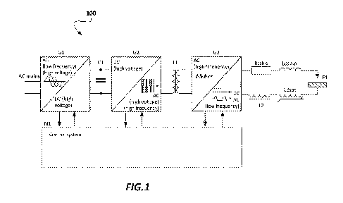
[0018] FIG. 1 presents a welding power supply 100, according to various
embodiments of the
disclosure. The welding power supply 100 may contain a primary converter,
shown as AC/DC
pre-converter Gl, a DC link with an energy buffer in form of the capacitor Cl,
a high frequency
primary converter, shown as primary converter G2, an isolating transformer Ti
with primary and
secondary windings, and an output converter G3.
[0019] The primary pre-converter G1 may receive a low frequency AC voltage
such as power
from a supplying means, such as an input mains power at 50 Hz or 60 Hz, and
output a DC link
6
CA 03063351 2019-11-12
WO 2018/234954 PCT/IB2018/054393
voltage, such as a high DC voltage. In some embodiments, the voltage that is
output by primary
pre-converter G1 may range between 100 V and 1000V. For example, in different
embodiments
the primary pre-converter G1 may or may not include a boost converter, buck-
boost converter,
controlled rectifier, to output a constant voltage DC link, independent of the
voltage received from
an AC input mains. In other embodiments, the primary pre-converter G1 may
output a DC
voltage on the DC link that is proportional to the AC input voltage received
by the primary
converter Gl. In certain embodiments, a primary pre-converter may perform a
role of an inverter,
transferring the energy from the DC link capacitor Cl to AC mains.
[0020] The primary converter G2 may operate at a high frequency, such as a
frequency greater
than 10 kHz, and in some examples, in the range of 10 kHz to 500 kHz or more.
The primary
converter G2 may operate as a voltage inverter (primary inverter) and may
receive DC voltage
from the DC link and output AC voltage of high frequency. The primary
converter G2 may also
operate as a rectifier and may receive AC current of high frequency generated
by the output
converter G3 from the isolating transformer Ti and output DC current to the DC
link. The
primary converter G2 may indirectly control the operation of the secondary
converter, that is, the
output converter G3, by means of forcing different states of the output of
isolating transformer.
The embodiments are not limited in this context.
[0021] The isolating transformer TI may receive high voltage, high frequency
AC voltage from
the primary converter G2 and convert the received high voltage to isolated
secondary high
frequency AC voltage, or may receive high frequency AC current from the output
converter G3
and output high frequency isolated AC current to the primary converter G2.
7
CA 03063351 2019-11-12
WO 2018/234954 PCT/IB2018/054393
[0022] The output converter G3 may operate as a rectifier and then may receive
isolated
secondary high frequency AC voltage and output DC voltage. The output
converter G3 may also
operate as a current inverter and then receive DC current and output high
frequency AC current.
In embodiments of known art of power supplies intended for AC welding due to
topology of the
output converter the operation in the mode of the current inverter is not
possible.
[0023] The output converter G3 may operate in both polarities of the output
voltage and both
directions of the output current. Consequently output converter G3 may output
DC voltage of
both polarities or output AC voltage of the low frequency, in the range of 10
Hz up to 1000Hz.
[0024] The output power receiver may contain electric arc welding load El
(including an
electric arc plasma, other conductive components of the welding) and serial
inductances of the
output inductor L2 and inductances of supplying cables Lcable. The welding
load is schematically
shown as an electrode and a base material. In particular embodiments, the
secondary side may
also comprise a saturating inductor L2sat or transformer, which components
make up an element
of the ignition system, needed for the start of the welding process without
short circuit of the
electrode to the base material. The output power receiver is specific to the
welding application,
but embodiments are not limited in this context. In particular, the output
power receiver can be
any power receiver or power receiver that can switch roles to act as a power
generator under
condition that the output comprise at least one serial inductor equivalent to
inductor L2.
[0025] A control system N1 governs switches in the primary converter G2 and
switches in the
secondary converter G3. In some embodiments the control system may also govern
the switches
in input AC/DC pre-converter Gl. This function does not alter the operation of
the present
embodiments.
8
CA 03063351 2019-11-12
WO 2018/234954 PCT/IB2018/054393
[0026] The primary converter G2 may control the power delivered to the
secondary side by
controlling the balance between the time of power delivery and time of idle or
free-wheeling state.
In a similar manner, the secondary converter G3 may control the power
delivered to the primary
side by the control of the balance between the time of power delivery and time
of free-wheeling
state.
[0027] FIG. 2 presents a more detailed depiction of one variant of the welding
power supply
100. In this view, the input mains AC/DC pre-converter, that is primary pre-
converter Gl, is
omitted for clarity, because the operation pre-converter G1 may not be related
to the present
embodiments of the disclosure. The primary converter G2 may be embodied in a
FB topology,
and is supplied from the primary DC link with an energy buffer ¨ capacitor Cl.
The FB topology
contains four active switches: VT1, VT2, VT3, and VT4, as well as four reverse
rectifiers: VD1,
VD2, VD3, and VD4. For illustrative purposes, active switches are shown in
FIG. 2 as insulated
gate transistor (IGBT), while the active switches may instead be formed using
any type of suitable
semiconductor switches. Isolating transformer Ti has one primary winding zl
and two secondary
windings z21 and z22, connected together with a central tap (CTAP). In further
embodiments, the
transformer Ti may have additional secondary windings. The central tap is
connected to the
output, to the power receiver. In particular embodiments the central tap is
connected to the output
inductor L2. Outer ends of the secondary winding are connected to four state
controlled
conductivity switches, shown as controlled switch VC5, and controlled switch
VC6. Four-state
controlled conductivity switch VC5 is made up of series connection of two
active switches, active
switch VT5, and active switch VT7, while four-state controlled conductivity
switch VC6 is made
up of series connection of two active switches, active switch VT6, and active
switch VT8. For
illustrative purposes the active switches are shown as Metal-Oxide
Semiconductor Field-Effect
9
CA 03063351 2019-11-12
WO 2018/234954
PCT/IB2018/054393
Transistors (MOSFET); in other embodiments the active switches (VT5-VT8) may
be formed
using any type of suitable semiconductor switches. Rectifiers VD5, VD6, VD7,
VD8 are
connected in parallel to the active switches VT5, VT6, VT7, VT8),
respectively, providing
reverse conductivity. Notably, the rectifiers providing reverse conductivity
may be embodied as
embedded parts of active switches.
[0028] In accordance with the present embodiments the four-state controlled
conductivity
switches (VCS and VC6) are capable of providing one of four states of
conductivity:
1. Bidirectional conductivity, enabling bidirectional power flow operation,
2. Conductivity in a first direction and blocking a current flow in a second
direction,
3. Conductivity in the second direction and blocking the current flow in the
first direction,
4. Blocking both directions of the current flow.
[0029] FIG. 3 shows another variant of the welding power supply 100. In this
variant, to
provide similar functionality, four-state controlled conductivity switch (VCS
and VC6) may
alternatively be embodied as a parallel connection of two controlled
rectifiers VS 5, VS7,
equivalent to thyristors, where VS5 can conduct current just in a first
direction and VS7 can
conduct current just in a second direction, opposite to the first direction. A
second pair of
controlled rectifiers, VS6 and VS8, is connected in the same way as controlled
rectifiers VS5,
VS7, as shown in FIG. 3.
[0030] FIG. 4
shows another variant of the welding power supply 100. In this example, the
controlled rectifiers, equivalent to thyristors as in FIG. 3, may be replaced
by other controlled
rectifiers in form of a series connection of a switch and a rectifier as
shown. As in any series
connection of two elements the order in series may be exchanged without a
change of the
CA 03063351 2019-11-12
WO 2018/234954 PCT/IB2018/054393
functionality. In comparison to the variant of FIG. 2, the output converter
circuit presented in FIG.
4 has no connections between the middle points between the active switch and
the rectifier. There
may be no substantial difference in operation of this alternative; notably, in
practical
implementation, the topology in FIG. 2 may provide lower conduction losses due
to available
reverse conductivity of switches. The last feature is typical of MOSFETs and
is not available for
IGBTs or bipolar transistors.
[0031] In order to provide increased voltage during changes of the current
direction and for
other purposes, the topology presented in FIG. 2 may be extended to a topology
presented in a
variant of welding power supply 100 shown in FIG. 5. Two additional, low power
windings z23
and z24, are added in this variant of transformer Ti and are connected to
outer ends of the
windings z21, z22. The increased voltage available on the outer ends of
windings z23, z24 may be
temporarily connected to the output by means of the additional controlled
rectifiers. These
additional controlled rectifiers are represented by the serial connection of
the rectifier VD9 and the
switch VT10, as well as by the rectifier VD1 1 and the switch VT12. By means
of operation of the
switches VT10 and VT12 instead of switches VT7 and VT8, an increased output
voltage of the
first polarity is available.
[0032] The topology presented in FIG. 5 can provide the increased voltage just
of the first
polarity, which topology may be insufficient for stabilization of the welding
process. A further
extension of topology is presented in FIG. 6. Four-state controlled
conductivity switches may be
connected to auxiliary windings z23, z24. As shown in FIG. 6, in comparison to
the topology of
FIG. 2, two auxiliary four-state controlled conductivity switches (that is, a
first auxiliary four-state
controlled conductivity switch and a second auxiliary four-state controlled
conductivity switch)
11
CA 03063351 2019-11-12
WO 2018/234954 PCT/IB2018/054393
are provided for this capability, embodied in components (VT9, VT10, VT11,
VT12, VD9, VD10,
VD11, VD12). In this way, increased voltage of both polarities may be
provided.
[0033] Turning now to FIGs. 7-16 there are shown different stages of exemplary
operation of a
welding power supply 100 arranged according to the variant of FIG. 2. Ten
different stages of the
converter may be defined, five for each direction of the output current. More
particularly, in the
various stages depicted in the figures to follow, the control system Ni may be
used to control and
synchronize the operation of switches in the primary converter G2 with the
operation of switches
in the output converter G3, as embodied in the variant of welding power supply
100 of FIG. 2. In
practical embodiments more different stages of operation may be defined. For
instance, if VT5,
VT6, VT7, VT8 switches are MOSFETs, which switches expose bipolar conductivity
in an ON
state, utilizing this feature may be effective. Then certain transitions
between stages may require a
short intermittent stage, in order to restore blocking capacity of the MOSFET
in a reverse
direction, when the current is intended to be conducted by one of the diodes
VD5, VD6, VD7,
VD8, but not by the respective parallel switch VT5, VT6, VT7, VT8. For
simplification of the
description of the operation, all switches are assumed ideal, having a
switching time equal to zero.
With such an assumption, the additional four stages can be omitted.
[0034] In a first stage and second stage, power transfer from the primary side
to secondary side
takes place for a first output voltage polarity and output current of the
first direction. Turning to
FIG. 7 there is shown the operation where two primary switches VT1 and VT4 are
switched on,
providing voltage on the primary side with the polarity as shown. A secondary
switch, VT7, is
switched on, secondary current flows through the z21 winding, VD5 rectifier
and VT7 switch. If
the VT5 switch has capability of reverse conductivity, as a MOSFET, this
switch may also
conduct, providing a parallel path for the secondary current, as depicted by
the dashed line.
12
CA 03063351 2019-11-12
WO 2018/234954 PCT/IB2018/054393
During stages 1, 2, and 3 both VT7 and VT8 switches may remain switched on.
Notably, during
stage 1 due to polarity of the voltage on the z22 windings, the VT8 switch
does not conduct
current.
[0035] Turning to FIG. 8, there is shown a stage 2, analogous to stage 1.
Primary switches
VT2 and VT3 are switched on, while primary and secondary voltages have
opposite polarity to the
polarity in stage 1. The secondary current flows through the winding z22,
rectifier VD6 and in a
case where VT6 conducts in reverse direction, also through switch VT6 and then
through the
switch VT8. The output voltage still has the first polarity and output current
still has the first
direction, as shown.
[0036] Turning to FIG. 9, there is shown a free-wheeling stage 3 ¨ free-
wheeling operation at
the current of the first direction. In this stage, all primary switches VT1,
VT2, VT3, and VT4 are
switched off. Since both switches VT7 and VT8 are switched on, the secondary
current flows in
parallel through the rectifiers, VD5 and VD6. In a case of application of the
reverse conducting
switches as MOSFETs, the current flows also through the switches VT5 and VT6.
[0037] In stages 4 and 5, power transfer takes place from the secondary to the
primary side,
where the power is of a second output voltage polarity and a first output
current direction, opposite
to the voltage polarity. In stages 4 and 5 all primary switches are switched
off Conduction on the
primary side is possible just through the primary rectifiers VD1, VD2, VD3,
VD4, which rectifiers
form a bridge rectifier. As shown in FIG. 10, in stage 4 the switch VT8 is
switched off Due to
energy accumulated in the output inductors, the secondary current flows in the
first direction.
Secondary current flows through the switch VT7, rectifier VD5 and secondary
winding z21.
Since neither secondary windings nor primary windings are short-circuited, the
secondary current
13
CA 03063351 2019-11-12
WO 2018/234954 PCT/IB2018/054393
is transformed to the primary side and flows back to the accumulating
capacitor Cl, via diodes
VD2 and VD3, forcing the voltage of the second polarity on the transformer's
winding. The
energy accumulated in inductors flows back to the input capacitor Cl
[0038] In analogous fashion to the scenario of FIG. 10, as shown in FIG. 11,
in stage 5 the
switch VT7 is switched off Due to energy accumulated in the output inductors,
the secondary
current flows in the first direction. Secondary current flows through the
switch VT8, rectifier VD6
and secondary winding z22. Since neither secondary windings nor primary
windings are short-
circuited, the secondary current is transformed to the primary side and flows
back to the
accumulating capacitor Cl, via diodes VD1 and VD4, forcing the voltage of the
second polarity
on the transformer's winding. The energy accumulated in inductors flows back
to the input
capacitor Cl.
[0039] In stage 6 and stage 7, shown in FIG. 12 and FIG. 13, respectively,
power transfer takes
place from the primary side to the secondary side, where the power is of a
second output voltage
polarity, and a of second output current direction corresponding to the
voltage polarity. Stages 6
and stage 7 are analogous to stages 1 and stage 2 but with reverse direction
of the output current
and reverse polarity the output voltage. Operation of the primary side
switches (VT1-VT4)
remains the same as for stage 1 and stage 2. Functioning of switches and
rectifiers of the
secondary side is swapped in pairs. On the secondary side, at stage 6 switches
VT5, VT6 and VT8
are switched on; due to polarity of the output voltage, the switch VT5 is not
conducting. Rectifier
VD8 is conducting in parallel with the switch VT8. At the stage 7 switches
VT5, VT6, and VT7
are switched on, while due to polarity of the output voltage, the switch VT6
is not conducting.
Rectifier. VD7 is conducting in parallel with the switch VT7.
14
CA 03063351 2019-11-12
WO 2018/234954 PCT/IB2018/054393
[0040] Turning to FIG. 14, there is shown a stage 8 corresponding to free-
wheeling operation at
the current of the second direction. In this stage, all primary switches VT1,
VT2, VT3, and VT4
are switched off Both switches VT5 and VT6 are switched on and the secondary
current flows in
parallel through the switches and rectifiers VD7, VT7 and VD8, VT8.
[0041] Turning now to FIG. 15 and FIG. 16, there are shown the stage 9 and
stage 10,
respectively. In these stages power transfer takes place from the secondary
side to primary side,
where the voltage is of a first polarity and an output current flows as a
reverse current in the second
direction, oppositely to the voltage polarity.
[0042] In stages 9 and 10 all primary switches are switched off Conduction on
the primary
side is possible just through the primary rectifiers VD1, VD2, VD3, VD4, which
rectifiers form a
bridge rectifier. As shown in FIG. 15, in stage 9 the switch VT6 is switched
off. Due to energy
accumulated in the output inductors, the secondary current flows in the second
direction.
Secondary current flows through the switch VT5, rectifier VD7 in parallel with
the switch VT7
and secondary winding z21. Since neither secondary windings nor primary
windings are short-
circuited, the secondary current is transformed to the primary side and flows
back to the
accumulating capacitor Cl, via diodes VD1 and VD4, forcing the voltage of the
first polarity on
the transformer's winding. The energy accumulated in inductors flows back to
the input capacitor
Cl.
[0043] In analogous fashion to the scenario of FIG. 15, as shown in FIG. 16,
in stage 10 the
switch VT5 is switched off Due to energy accumulated in the output inductors,
the secondary
current flows in the first direction. Secondary current flows through the
switch VT6, rectifier VD8
in parallel with the switch VT8 and secondary winding z22. Since neither
secondary windings nor
primary windings are short-circuited, the secondary current is transformed to
the primary side and
CA 03063351 2019-11-12
WO 2018/234954 PCT/IB2018/054393
flows back to the accumulating capacitor Cl, via diodes VD2 and VD3, forcing
the voltage of the
first polarity on the transformer's winding. The energy accumulated in
inductors flows back to the
input capacitor Cl.
[0044] Notably, the welding power supplies of the embodiments as disclosed
herein may operate
in other stages, related to the non-ideality of a real electric circuit,
understood as the presence of
parasitic capacitors and stray inductances, and the necessity in establishing
the conduction and
restoration of the blocking capacity in semiconductor devices. Since those
stages are not germane
to the present embodiments the stages will be not included in the present
description. In practical
embodiments, these stages may be taken into consideration.
[0045] In various embodiments, welding may be performed over a plurality of
welding cycles
such as AC welding cycles, where a given welding cycle includes a series of
operation modes. A
given welding cycle may span a duration of a few milliseconds to tens of
milliseconds in some
embodiments. The embodiments are not limited in this context. During a given
operation mode a
sequence of stages may be performed, based upon the stages shown in FIGs. 7-
16, for example. In
various embodiments, the sequence of stages may be performed multiple times
within a given
operation mode.
[0046] In one embodiment, the operation mode of power delivery with a first
polarity (mode I)
is conducted according to the sequence of stages: 1-3-2-3-1-3-2-3-.... The
average output voltage
of a first polarity, and consequently the power and the output current, may be
controlled by the
principle of pulse width modulation (PWM), where the ratio between periods of
delivery of the
energy from the primary side and free-wheeling periods, when the energy from
the primary side is
not delivered, is regulated. In this way, average output voltage of a given
polarity can be regulated
from zero to certain maximum. The period of the operation, measured by the sum
of times of
16
CA 03063351 2019-11-12
WO 2018/234954 PCT/IB2018/054393
consequent stages: 1, 3, 2 and next stage (3) may have duration between 100
[IS down to 10 [IS or
less, and may be constant or may vary, depending on the variation of the type
of the applied PWM
control method. In practical embodiments sequence 1-3-2-3-1-3-2-3-.... of the
mode I may include
additional stages required because of imperfection of semiconductor devices,
which devices need
certain time for acquiring state of the conduction and certain time for
restoration of the blocking
state as well as due to presence of the parasitic components in the circuit.
[0047] In further embodiments, if required by certain conditions, the
operation mode of power
recovery (recuperation) for a first polarity of the output current (mode IV)
may be conducted
according to the sequence of stages: 4-3-5-3-4-3-5-3 ... The power accumulated
in the output
inductors is transferred to the input, while the output current has a first
direction. The principle of
PWM may be applied in the mode IV for regulating the ratio between power
reverse stages, that is,
recuperation stages 4 and 5, and the free-wheeling stage 3. In this way the
average output voltage
of the second polarity can be controlled in the presence of the output current
of the first direction in
an analogous way as control is performed in the mode I. In further
embodiments, the mode IV
sequence may also include stages 1 and 2 for commutation purposes. During the
transition from the
free-wheeling stage 3 to recuperation stage 4 or 5 termination of the
secondary current by means of
the secondary switches due to leakage inductance of the transformer may not be
desirable.
Therefore, the stage 1 or stage 2 is applied for a relatively short time, just
to force the output current
to flow just through the one winding z21 or z22. The respective secondary
switch VT7 or VT8 is
switched off in a zero current switching condition (ZCS) starting the
respective recuperation stage,
recuperation stage 4 or 5. When stages 1 and 2 are applied in the mode IV, the
sequence of the
stages may be as follows: 3-1-4-3-2-5-3-1-4-3-.... The last sequence may be
extended further by
additional stages required because of parasitic components in the circuit as
well as non-ideality of
17
CA 03063351 2019-11-12
WO 2018/234954 PCT/IB2018/054393
semiconductor devices. For example, such devices need a certain time for
acquiring a state of
conduction, and a certain time for restoration of the blocking state.
[0048] In further embodiments, the operation mode of power delivery with a
second polarity
(mode 111) is conducted according to the sequence of stages: 6-8-7-8-6-8-7-8-
.... The output voltage,
and consequently the power and the current is controlled by the principle of
pulse width modulation
(PWM), where a ratio between periods of delivery of the energy and free-
wheeling periods may be
controlled in the same manner as for the mode I. The mode III may require
additional stages in the
sequence of control in the same way as may be required for the mode I.
[0049] In further embodiments, the operation mode of power recovery for a
second direction of
the output current (mode II) is conducted according to the sequence of stages
8-9-8-10-8-9-8-10-8-
... . The power accumulated in the output inductors is transferred to the
input and the output current
has a second direction. The mode II sequence may also require an addition of
stages 6 and 7 for
switching off switches VT5 and VT6 in ZCS condition. When stages 6 and 7 are
applied in the
mode II, the sequence of the stages may be as follows: 8-7-9-8-6-10-8-7-9-8-6-
10-8-... The last
sequence may be extended further by the additional stages required because of
parasitic components
in the circuit and non-ideality of semiconductor devices, as noted above.
[0050] In an additional embodiment, the operation of converters having
topologies depicted in
FIG. 5 with additional windings z23 and z24, involves the same delivery of
power to the welding
load during mode I and mode III, or during recovery modes: mode IV or mode It
An additional
mode of operation, mode le may be added to listed modes I, IV, III and It The
mode le, where the
power is delivered to the load and the voltage of the first polarity is
increased due to employment of
serially connected additional windings of the transformer Ti. The mode employs
an active rectifier,
which device includes rectifiers VD9, VD ii and switches VT10, VT12.
Rectifiers VD10 and VD12
18
CA 03063351 2019-11-12
WO 2018/234954 PCT/IB2018/054393
are embedded parts of the devices, but do not play an active role in the
present topology. The mode
le include 3 stages similar to stages in the mode I. Stage 11 is an analog to
stage 1. On the primary
side, switches VT1 and VT4 are switched on. On the secondary side, switches
VT10 and VT12 are
switched on too. The voltage of the first polarity and increased level equal
the voltage on the both
windings z21 and z23 appears on the output. The output current of the first
direction flows through
the rectifier VD9 and the switch VT10. Similarly, in stage 12, analog to stage
2, primary side
switches VT2, VT3 are switched on. The output voltage has the first polarity
and increased value
equal the voltage on the both windings z22 and z24. The output current of the
first direction flows
through the rectifier VD11 and the switch VT12. Free-wheeling stage 13 is
similar to the stage 3.
All switches on the primary side are off Transformer output is shorted because
the output current
of the first direction flows simultaneously through the both rectifiers VD9
and VD11 and the both
switches VT10 and VT12. The mode le is similar to the mode I. The sequence of
stage is 11-13-
12-13-11-13- ... The average output voltage of the first polarity may be
regulated using the same
principle of the PWM as in previous four modes.
[0051] The utilization of the additional windings z23 and z24 and active
rectifier that
includes rectifiers VD9, VD11 and switches VT10, VT12 as presented in FIG. 5
enables an
operation in the mode IVe similar to the mode IV, where the average output
voltage has the
second polarity and the output current flows in the first direction. The
difference between
mode IV and mode IVe is that the switches VT5, VT6, VT7, VT8 are permanently
off,
rectifiers VD5, VD6, VD7, VD8 are not conducting. The mode IVe includes the
same free-
wheeling stage, free-wheeling stage 13, where all for devices VD9, VD11, VT10,
VT12 are
conducting simultaneously. In the next stage, stage 14, the output current of
the first direction
flows just through the rectifier VD9 and switch VT10. The switch VT12 is
switched off. In
19
CA 03063351 2019-11-12
WO 2018/234954 PCT/IB2018/054393
this stage voltage of the second polarity and increased value appears on the
output. The output
current is transformed to the primary side and flows through the rectifiers
VD2 and VD3 to the
DC link capacitor Cl. Similarly, in the stage 15 the output current of the
first direction flows
through the rectifier VD11 and switch VT12, while the switch VT10 is switched
off. The
output current is transformed to the primary side and flows to the capacitor
Cl through the
rectifiers VD1 and VD4. Basically, the mode IVe is a sequence 13-14-13-15-13-
14-... The
mode IVe may require implementation of additional stages except the stage 13,
stage 14 and
stage 15. While in the mode IVe primary switches are not intended to operate,
they may be
employed to force the ZCS condition for switching off the switches VT10 and
VT12 on the
transition between free-wheeling stage 13 and the recuperation stages, that
is, stage 14 and
stage 15.
[0052] In further embodiments, utilization of the additional windings z23 and
z24 and active
rectifier that is made of rectifiers VD9, VD11 and switches VT10, VT12 as
depicted on the FIG.
may require more stages of operation for transitions between operation with
additional
windings and the operation without additional windings. In particular,
additional stages with
utilization of the primary switches may be applied to force ZCS condition for
switching off
switches VT10 and VT12 during transition to the free-wheeling stage with
utilization of the
windings z21, z2 and switches VT5, VT6, VT7, VT8, and rectifiers VD5, VD6,
VD7, VD8.
[0053] In additional embodiments, the operation of converters having
topologies depicted in
FIG. 6 with additional windings z23 and z24, involves the same delivery of
power to the welding
load during mode I and mode III, or during recovery modes IV or II, where the
switches and
rectifiers VT5, VT6, VT7, VT8 and VD5, VD6, VD7, VD8 are substituted by VT9,
VT10, VT11,
VT12, VD9, VD10, VD11, VD12, respectively. This topology enables modes le and
IVe as
CA 03063351 2019-11-12
WO 2018/234954 PCT/IB2018/054393
described for the topology on the FIG. 5. In the embodiment according to FIG.
6 a mode he,
analogous to the mode Ie, have a place, when the output voltage has a second
polarity and an
extended value due to use of the additional windings z23 and z24 and the
second direction of the
output current. The mode Me includes basically three stages: free-wheeling
stage 16 ¨ free-
wheeling of the second direction of the output current, stage 17 ¨ power
delivery with output voltage
of the second polarity and the current of the second direction flowing through
the switch VT9 and
the rectifier VD10, stage 18, with output voltage of the second polarity and
the current of the second
direction flowing through the switch VT11 and the rectifier VD10.
[0054] Consequently, a further embodiment according to FIG. 6 may provide a
mode He,
analogous to the mode We, where current has a second direction and the output
voltage has a first
polarity. Mode He may operate similarly to mode IVe, except the free-wheeling
stage 16 may
include stages 19 and 20, when the energy accumulated in the output
inductances goes back to the
capacitor Cl. Mode He may similarly include additional stages with utilization
of the primary
switches VT1, VT2, VT3, VT4 in purpose to force ZCS for switching off the
switches VT9 and
VT11. Similarly to topology presented in FIG. 5 operation of the present
topology may require
additional stages during the transitions to the free-wheeling stage with
employment of just z21 and
z22 windings and devices VT5, VT6, VT7, VT8, VD5, VD6, VD7, VD8.
[0055] Power converters of embodiments presented in EEGs. 2, 3, 4, 5, 6 are
capable of operating
in modes I. IV, III, IV, which modes are equal to operation in quadrants I, W,
III, II on the plane of
output voltage and current. Those converters can deliver power of the first
and second polarity of
the output voltage and reverse the voltage to transfer energy from the
secondary to primary side. In
particular, in welding applications those converters can be utilized for
unipolar power delivery, for
power supplies that can reverse of the output voltage, for power supplies
where the acceleration of
21
CA 03063351 2019-11-12
WO 2018/234954 PCT/IB2018/054393
the transitions of the current transpires without changing the direction of
the current, but with the
reverse of the voltage and eventually, to deliver low frequency AC output
power with capacity of
fast current transitions. The alternating current application covers all other
applications, and thus
will further described solely.
[0056] Alternating current operation of the converter is the sequence for all
four modes: mode I,
mode IV, mode III, mode II. Depending on topology employed, and the needs of
operation, an
extended voltage may be applied in all modes during the current transitions.
Then modes Ie, IVe,
Me, IIe may be employed for a temporary increase of voltage and speed up of
transition of the
current. Modes IV and II in welding applications may or may not be applied.
The role of those
modes is to speed up the current transitions. If converters of the presented
topologies are used in
applications different than welding, in particular, in application to the
loads that may change the role
from the consumer of the energy to deliverer of the energy, modes IV and II
may be employed even
for permanent conversion with energy flow from the load to the input.
[0057] Exemplary timing diagrams of operation in the AC operation are
presented in FIG. 17.
The diagrams present the operation of the converter of the topology with
unipolar extended voltage
as shown in FIG. 5. A plurality of welding cycles are shown as Tad, Tac2,
Tac3, Tac4, where in
a given welding cycle, the sequence of the operation modes is: mode I ¨ mode
IV ¨ mode III ¨ mode
II ¨ mode I ¨ mode IV ..... As an example in FIG. 17 the extended voltage was
applied just in
mode Ie in purpose to speed up the current transition. Therefore, the FIG. 17
time diagram is
applicable to the topology presented in FIG. 5 or FIG 6. Extended voltage can
be used also during
the other transitions, in purpose to accelerate the change of the output
current. Converter of topology
presented in the FIG. 5 may employ also mode IVe, while converter of topology
presented in the
22
CA 03063351 2019-11-12
WO 2018/234954 PCT/IB2018/054393
FIG. 6 may additionally utilize modes he and He. For simplicity those
instances were not presented
on the FIG. 17.
[0058] In summary, the present embodiments provide novel architecture and
methods for
operating power supplies in four quadrants. In one embodiment a primary
converter of a power
supply may include a full bridge converter (full bridge inverter) comprising
four active
switches and four rectifiers, and an isolating transformer with secondary
winding that has two
ends and central tap, and an output converter may comprise two four state
controlled
conductivity switches.
[0059] In a further embodiment, the four state controlled conductivity
switches of the output
converter may comprise two controlled rectifiers connected in parallel, or
switches of one
direction controlled conductivity connected in series with each other and each
connected in
parallel with a rectifiers, providing a reverse conductivity.
[0060] In another embodiment, the isolating transformer may comprise two
auxiliary
windings, and the output converter may comprise two auxiliary controlled
rectifiers or two four
state controlled conductivity switches, providing capacity of temporary
increase of the output
voltage, respectively in one polarity or in both polarities of the output
voltage.
[0061] In another embodiment, a method of operating a power supply for welding
or other
purposes may include operation in four modes of operation, providing regulated
output voltage
of two polarities, regulated reverse power flow of two directions of an output
current, and by
combination of available modes of operation providing an alternating current
output of a low
frequency.
[0062] The present disclosure is not to be limited in scope by the specific
embodiments
described herein. Indeed, other various embodiments of and modifications to
the present
23
CA 03063351 2019-11-12
WO 2018/234954 PCT/IB2018/054393
disclosure, in addition to those described herein, will be apparent to those
of ordinary skill in
the art from the foregoing description and accompanying drawings. Thus, such
other
embodiments and modifications are intended to fall within the scope of the
present disclosure.
Furthermore, although the present disclosure has been described herein in the
context of a
particular implementation in a particular environment for a particular
purpose, those of ordinary
skill in the art will recognize that its usefulness is not limited thereto and
that the present
disclosure may be beneficially implemented in any number of environments for
any number of
purposes. Thus, the claims set forth below are to be construed in view of the
full breadth and
spirit of the present disclosure as described herein.
24