Note : Les descriptions sont présentées dans la langue officielle dans laquelle elles ont été soumises.
DESCRIPTION
ULTRA HIGH-SENSITIVITY MICRO MAGNETIC SENSOR
Field
[0001] The present invention relates to a technology of
improving sensitivity characteristics of a GSR sensor by
adopting rising pulse detection.
Here, the GSR sensor is an ultra high-sensitivity micro
magnetic sensor based on the GHz spin rotation effect.
Background
[0002] The high-sensitivity micro magnetic sensor includes
a horizontal FG sensor, a vertical FG sensor, a hole sensor,
a GMR sensor, a TMR sensor, a MI sensor, a GSR sensor, a high
frequency carrier sensor, and the like. These sensors are
currently used widely in smartphones, vehicles, medical
treatment, robots, and the like. Among the above-described
sensors, the GSR sensor is excellent in sensitivity and size,
and draws the most attention.
[0003] To achieve remote control of an in-vivo motion
device, an investigation is currently advanced for finding a
position and a direction by providing a three-dimensional
magnetic sensor utilizing a GSR sensor.
The sensor is preferably smaller to provide it in a
motion device. However, the detection sensitivity is
deteriorated inversely proportional thereto. Furthermore,
1
Date Recue/Date Received 2021-06-10
with the restriction of a supply power source, the reduction
of power consumption during measurement has been demanded.
Citation List
Patent Literature
[0004] Patent Literature 1: Japanese Patent No. 5839527
Brief Description of the Drawings
[0005] Fig. 1 is a plane view of a GSR sensor element
according to an embodiment and an example,
Fig. 2 is a section view of the GSR sensor element along
line A1-A2 of Fig. 1,
Fig. 3 is an electronic circuit diagram according to the
embodiment and the example,
Fig. 4 is a relational diagram between the pulse time
and the pulse current application according to the embodiment
and the example,
Fig. 5 is a waveform chart of a coil voltage when a
pulse current is applied according to the embodiment and the
example,
Fig. 6 is an output waveform chart according to the
embodiment and the example,
Fig. 7 is a diagram of an output V when two magnetic
wires are subjected to a pulse current in opposite directions
(+ direction and - direction) when the external magnetic
field H = 0,
2
Date Recue/Date Received 2021-06-10
Fig. 8 is a diagram of an output V when the external
magnetic field H = -2G to +2G,
Fig. 9 is a relational diagram between the external
magnetic field H and impedance Z,
Fig. 10 is an output diagram of the coil voltage in
rising pulse detection and falling pulse detection with one
magnetic wire and two magnetic wires,
Fig. 11 is an explanatory diagram of the linearity P in
relation between the change of the external magnetic field
and the output, and
Fig. 12 is a relational diagram between the magnetic
field Hx and a deviation amount in the rising pulse of the
GSR sensor.
Summary
Technical Problem
[0006] As the detection method by the GSR sensor, there
exist two methods of rising pulse detection and falling pulse
detection. In rising pulse detection, the magnetic field
sensitivity is about 2.5 times as high as that of falling
pulse detection, which shortens pulse time and reduces power
consumption. However, the linearity is about 1 to 2% and is
inferior to that of falling pulse detection of 0.5% or lower.
The invention aims at making the most use of advantages
of rising pulse detection while making its linearity 0.5% or
3
Date Recue/Date Received 2021-06-10
lower.
[0007] A coil output voltage (hereinafter, referred to as
a coil voltage) of the GSR sensor includes two kinds of
voltages of an induced voltage dependent on a pulse current
(referred to as an "a voltage") and a voltage dependent on an
external magnetic field (referred to as a "b voltage"). In
comparison between rising pulse detection and falling pulse
detection, two voltage peaks are more adjacent to each
other in the case of falling pulse detection, and the
influence by a pulse current is larger. Moreover, the MI
effect changes the impedance of magnetic wires by a magnetic
field. As a result, the "a voltage" dependent on a pulse
current is also influenced by the magnetic field, and may not
be canceled easily. That is, if the "a voltage" is not
influenced by a magnetic field, the "a voltage" may be
measured with H = OG, and a net b voltage may be thus
detected by cancelling the "a voltage".
[0008] The investigation for removing an induced voltage
dependent on a pulse current from a coil voltage found by
rising pulse detection has been performed for 20 years.
However, it remains an unsolved difficult problem.
Solution to Problem
[0009] The inventors found that if two magnetic wires are
arranged in one coil and a pulse current is applied in
4
Date Recue/Date Received 2021-06-10
opposite directions, a coil induced voltage of rising pulse
detection becomes 0 when H = 0 G (Fig. 7). It is recognized
that if an electric current is applied in opposite directions
in the case where a magnetic field H exists, the coil voltage
is not changed and only the "b voltage" is detected (Fig. 8).
That is, the "a voltage" is apparently disappeared.
Furthermore, in the measurement of the "b voltage" while
changing a magnetic field, they found that the voltage is
linearly output symmetrically relative to the
positive/negative of the magnetic field with the linearity of
0.3% or lower, which is excellent.
Even when the magnetic field H is changed from zero, the
"a voltage" is disappeared. This is apparently because the
impedance of two wires is changed symmetrically relative to
the magnetic field H, regardless of a direction of an
electric current, and thus the impedance thereof is
constantly same and a pulse current flowing in the two wires
is same, which cancels the influence on their coils even when
a magnetic field is changed (Fig. 9).
[0010] In the case of rising pulse detection, the
detection is performed with rising, which allows pulse time
of 1 ns (1 nanosecond) or shorter. Meanwhile, in the case of
falling pulse detection, the detection needs to be performed
after the rising coil voltage is attenuated completely. Thus,
Date Recue/Date Received 2021-06-10
the pulse time needs to be maintained for about 10 ns.
Therefore, if the rising pulse detection is adopted, the
pulse current consumption may be 1/10 or smaller.
[0011] The coil voltage of the element including two
magnetic wires of the invention is twice the coil voltage of
the element including one magnetic wire. Moreover, the coil
voltage in rising pulse detection is 2.5 times the coil
voltage in falling pulse detection (Fig. 10). As compared
with the GSR sensor described in Patent Literature 1, the
coil voltage is five times with the element of the same size.
[0012] It is confirmed that the relation between the coil
voltage and the external magnetic field is same as the
equation in the GSR sensor described in Patent Literature 1.
That is,
Vs = Vo.2L.nD.p.Nc.f.sin(nH/2Hm) ................ (1)
[0013] Here, Vs is a coil voltage, and Vo is a constant of
proportionality determined by wire magnetic permeability,
magnetic characteristics of wire materials with saturation
magnetic flux density, and a pulse current. As a control
factor constant, L is a wire length, D is a wire diameter, p
is a skin depth of a pulse current, Nc is the number of
winding of a coil, f is a pulse frequency, H is an external
magnetic field, Hm is an external magnetic strength to obtain
the maximum coil output voltage.
6
Date Recue/Date Received 2021-06-10
[0014] By applying arcsine transformation to both sides of
the equation (1) and letting the resulted value to be a
conversion voltage V', the following equations (2) and (3)
are obtained:
V' = arcsin(Vs/Vo.2L.nD.p.Nc.f) = (n.1/2Hm) .H .................. (2)
H = 2Hm/nxV' ......... ( 3 )
H is found on the basis of the expression (3).
V' is changed linearly from -Hm to +Hm relative to the
magnetic field H. The measurement range is Hm, and is about
four times that in the case without arcsine transformation.
Note that when VX = a(1-A)Hx, the linearity P is defined as P
= 100xA (%).
That is, the linearity is defined on the basis of a deviation
amount A from the equation Vx = aHx when A = 0.
[0015] Furthermore, it is confirmed that the linearity is
0.2%, which is more preferable than 0.5% that is a deviation
amount of a falling pulse of the GSR sensor (Fig. 12).
The GSR sensor strengthens electromagnetic coupling
between the magnetic wire and the coil with the interval
between the magnetic wire and the coil inner diameter of 3 pm
or smaller. Also in the invention, the same relation remains
except for the interval between the two magnetic wires.
[0016] The same electronic circuit as in Patent Literature
1 is adopted. The pulse frequency of a pulse current applied
7
Date Recue/Date Received 2021-06-10
to the magnetic wire is 0.2 GHz to 4 GHz. The pulse current
has the strength required to generate on the surface of a
magnetic wire over a 1.5 times larger circumferential
magnetic field than the magnetic anisotropy field.
The coil voltage occurring at the time of pulse
energization is fed to a sample hold circuit through a pulse
compliant buffer circuit. With the small number of winding
of the coil, the coil voltage may be fed directly to the
sample hold circuit.
[0017] The rising pulse is detected using an electronic
switch at the peak timing of a coil output waveform. The "a
voltage" does not exist, and thus the temporal timing of the
peak voltage is constant without being dependent on the
magnetic field H. However, if the "a voltage" exists, the
peak timing is changed depending on the magnetic field H.
Thus, strictly speaking, it is not possible to adjust the
detection at the peak timing of a coil output waveform. This
causes nonlinearity.
The capacitor capacitance of the sample hold circuit is
4 pF to 100 pF. it is preferable that the intervals between
on and off of the electronic switch is shortened as much as
possible to also reduce the capacitor capacitance to 4 pH to
8pH. In this manner, the voltage at the peak timing is held
by the capacitor as an instantaneous voltage value. The held
8
Date Recue/Date Received 2021-06-10
capacitor voltage is output through a programming amplifier.
Advantageous Effects of Invention
[0018] The rising pulse detection type GSR sensor achieves,
with the same element size, five times magnetic field
detection sensitivity and 1/10 or less power consumption,
enabling considerable downsizing of the magnetic sensor with
an in-vivo motion device.
Description of Embodiments
[0019] An embodiment of the invention is described as
follows.
Note that one, or two or more configurations arbitrarily
selected from the specification may be added to the
configuration of the invention. The most preferable
embodiment varies depending on a subject and required
characteristics.
[0020] A GSR sensor that is an ultra high-sensitivity
micro magnetic sensor according to the invention includes
a magnetic field detection element including two
conductive magnetic wires for magnetic field detection
arranged adjacent to each other on a substrate, a round coil
wound around the two magnetic wires, two electrodes for wire
energization, and two electrodes for coil voltage detection,
a means for applying a pulse current to the magnetic wires, a
circuit for detecting a coil voltage occurred when the pulse
9
Date Recue/Date Received 2021-06-10
current is applied to the magnetic wires in opposite
directions, and a means for converting the coil voltage into
an external magnetic field H,
in which the magnetic wire has a magnetic anisotropy
field of 20 G or less, with a two-phase magnetic domain
structure of a surface magnetic domain with circumferential
spin alignment and a center core magnetic domain with
longitudinal spin alignment, and
the pulse current applied to the magnetic wire has a
pulse frequency of 0.2 GHz to 4 GHz and a strength required
to generate over a 1.5 times larger circumferential magnetic
field than the anisotropy field on a surface of the wire, and
the coil has a coil pitch of 10 pm or less. The average
inner diameter of the coil is preferably 35 pm or smaller.
In the case where a plurality of pairs of wires are
arranged, the interval between the coil and the magnetic wire
is preferably 1 pm to 5 pm.
[0021]
Moreover, in the GSR sensor that is the ultra high-
sensitivity micro magnetic sensor according to the invention,
the pulse current is applied to the magnetic wire, and
the circumferential spin inclined in an axial direction is
subjected to super high speed rotation by a wire axial
magnetic field in the surface magnetic domain, to take out
only a magnetization change in the wire axial direction due
Date Recue/Date Received 2021-06-10
to a super high speed rotation phenomena occurred at the
rotation and perform conversion into a field H using an
equation (1):
Vs - Vo-2L-nD-p-Nc-f-sin(nH/2Hm) ........... (1)
where Vs is a coil output voltage and Vo is a constant of
proportionality, and as a control factor constant, L is a
wire length, D is a wire diameter, p is a skin depth of a
pulse current, Nc is the number of winding of a coil, f is a
pulse frequency, Hm is an external magnetic strength to
obtain a maximum coil output voltage.
[0022] Furthermore, the GSR sensor that is the ultra high-
sensitivity micro magnetic sensor according to the invention
further includes an electronic circuit including a pulse
generating circuit for generating the pulse current, an input
circuit for inputting a coil voltage, a pulse compliant
buffer circuit, a sample hold circuit with an electronic
switch for detecting a peak voltage of an output waveform of
the coil voltage and a capacitor with a capacitance of 4 to
100 pF for holding the peak voltage, and an programming
amplifier for amplification before AD (analog-digital)
conversion.
[0023] The embodiment of the invention will be described
in detail with reference to Fig. 1 to Fig. 6.
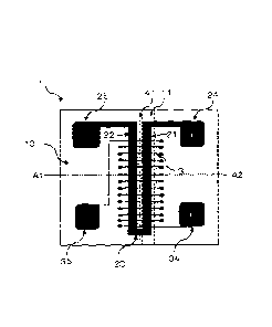
The GSR sensor element (hereinafter, referred to as an
11
Date Recue/Date Received 2021-06-10
element) 1 includes, on a substrate 10, two magnetic wires
(21 and 22), one coil 3 wound around the two magnetic wires,
two electrodes (24 and 25) for wire energization, two
electrodes (34 and 35) for coil voltage detection, a
connection part between the magnetic wires and the wire
energization electrodes, and a connection part between the
coil and the coil voltage detection electrodes. Moreover,
the element 1 includes a means 23 for applying a pulse
current to the two magnetic wires (21 and 22) in opposite
directions. Then, the element 1 further includes a circuit 5
for detecting a coil voltage occurred when a pulse current is
applied and a means for converting a coil voltage into an
external magnetic field. The external magnetic field H and
the coil voltage Vs are expressed by the mathematical
relation of the above-described expression (1).
[0024] < Structure of element >
The structure of the element 1 is as illustrated in Fig.
1 and Fig. 2.
The size of the element 1 is 0.07 mm to 0.4 mm in width
and 0.25 mm to 1 mm in length, which is the size of the
substrate 1. In the center part of the element 1, the
substrate 10 has a groove of 20 to 60 pm in width and 2 to 20
pm in depth so that the two magnetic wires (21 and 22) are
aligned and disposed in parallel to each other. The two
12
Date Recue/Date Received 2021-06-10
magnetic wires (21 and 22) are adjacent to each other with
the interval of 1 to 5 pm. It is preferable that the
magnetic wires (21 and 22) are isolated from each other by an
insulating material, such as an insulating separation wall,
for example.
[0025] < Magnetic wire >
The magnetic wire 2 is formed of a CoFeSiB amorphous
alloy with a diameter of 5 to 20 pm. The periphery of the
magnetic wire 2 is preferably coated with an insulating
material, such as insulating glass, for example. The length
is 0.07 to 1.0 mm.
The magnetic wire 2 has a magnetic anisotropy field of
20 G or less, with a two-phase magnetic domain structure of a
surface magnetic domain with circumferential spin alignment
and a center part core magnetic domain with axial spin
alignment.
[0026] < Coil >
In the coil 3, it is preferable that the number of
winding of the coil is 6 to 180 times and the coil pitch is 5
pm. The interval between the coil 3 and the magnetic wire 2
is preferably 3 pm or smaller. The average inner diameter of
the coil is preferably 10 to 35 pm.
[0027] < Manufacturing method of element >
The manufacturing method of the element is described
13
Date Recue/Date Received 2021-06-10
with reference to Fig. 2.
Electrode wiring is performed on a lower coil 31 and the
substrate surface along the groove 11 formed on the substrate
10. Then, an insulating separation wall 41 is formed in the
center part of the groove 11 to have a two-groove form, and
each of the two magnetic wires 21 and 22 coated with glass is
arranged therein. Next, an insulating resist is applied to
the entire surface of the substrate. Thus, the magnetic
wires 21 and 22 are fixed in the groove 11. The insulating
resist is applied thinly onto the upper part of the magnetic
wires 21 and 22. At that part, an upper coil 32 is formed by
a photolithographic technology.
In the case where the magnetic wires 2 not coated with
glass are used, an insulating material 4 needs to be
preliminarily applied to prevent electrical contact between
the lower coil 31 and the magnetic wires 21 and 22.
[0028] In the manufacturing of the coil, the recessed
lower coil 31 is formed along the groove surface and the both
sides of the groove 11 formed on the substrate 11. The
projecting upper coil 32 is electrically jointed to the lower
coil through a joint part 33 to form the spiral coil 3.
[0029] At the ends of the two magnetic wires 21 and 22,
glass as an insulating film is removed to allow electrical
connection by metal vapor deposition.
14
Date Recue/Date Received 2021-06-10
[0030] < Magnetic wire and coil wiring structure >
In the wiring structure of the magnetic wire 2, the wire
input electrode (+) 24 is connected to the upper part of the
magnetic wire 21, and the lower part of the magnetic wire 21
is connected to the lower part of the magnetic wire 22
through the wire connection part 23, as illustrated in Fig. 1.
The upper part of the magnetic wire 22 is connected to the
wire output electrode (-) 25. This wire connection part 23
enables a downward flow of a pulse current from the upper
part to the lower part in the magnetic wire 21, and an upward
flow of a pulse current from the lower part to the upper part
(in the opposite direction from the direction in the magnetic
wire 21) in the magnetic wire 22.
[0031] In the wiring structure of the coil 3, the coil
output electrode (+) 34 is connected to the lower end part of
the coil 3, and the upper end part of the coil 3 is connected
to a coil ground electrode (-) 35, as illustrated in Fig. 1.
[0032] < Electronic circuit >
An electronic circuit 5 includes a pulse generating
circuit 51 for generating a pulse current, an input circuit
53 for inputting a coil voltage, a pulse compliant buffer
circuit 54, the sample hold circuit with an electronic switch
56 for detecting a peak voltage of an output waveform of a
coil voltage and a capacitor with a capacitance of 4 to 100
Date Recue/Date Received 2021-06-10
pF for holding a peak voltage, and an amplifier 58. The
amplifier 58 includes a programming amplifier for
amplification before AD conversion.
Moreover, the GSR sensor element is connected to output
a coil voltage of the electronic circuit 5.
[0033] At a pulse frequency of a pulse current of 0.2 to 4
GHz, the pulse current strength is 50 to 200 mA and the pulse
time is 0 to 2 nsec. Fig. 4 illustrates the relation between
the elapse of energizing time and the application of a pulse
current when the pulse current is applied to the GSR sensor
element. In the example of Fig. 4, the pulse current rises
in 0.5 nsec from the start of energization, and this applied
state is kept for given pulse time of 0.5 nsec. Once such
energization is cut off, the pulse current falls in 0.5 nsec.
[0034] < Waveform of coil voltage >
Fig. 5 illustrates a waveform chart of a coil voltage
when the above-described pulse current is applied.
In the invention, the timing of a peak voltage is
detected. The electronic switch is turned on and off
repeatedly with the opening-closing time of 0.1 to 1.5 nsec.
[0035] The capacitor capacitance of the sample hold
circuit is 4 to 100 pF, and the AD conversion of the
electronic circuit is 14 to 16 bits. Note that to shorten
the interval of the on and off of the electronical switch,
16
Date Recue/Date Received 2021-06-10
the capacitor capacitance is preferably 4 to 8 pF.
In the coil output, the sensitivity is 50 mV/G to 3 V/G
in the measurement range of 3 to 100G with a sin wave output,
as illustrated in Fig. 6. The linearity is 0.3% or lower.
[0036] < Example >
Fig. 1 illustrates a plane view of the GSR sensor
element according to the example. Fig. 2 illustrates a
section view thereof. Fig. 5 illustrates an electronic
circuit. The GSR sensor of the invention includes the GSR
sensor element 1 having the two magnetic wires (21 and 22),
the one coil 3 wound around the two magnetic wires, the two
electrodes (24 and 25) for wire energization, and the
electrodes (34 and 35) for coil voltage detection, the means
for applying a pulse current to the magnetic wire 2, the
circuit for detecting a coil voltage occurred when the pulse
current is applied, and the means for converting a coil
voltage into an external magnetic field H. The external
magnetic field H and the coil voltage are expressed in the
mathematical relation shown in the expression (1).
[0037] The size of the element 1 is 0.12 mm in length and
0.20 mm in width. The groove 11 on the substrate 10 is 40 pm
in width and 8 pm in depth. The wire interval is 3 pm.
[0038] The magnetic wire (21 and 22) is formed of a
CoFeSiB amorphous alloy coated with glass of 10 pm in
17
Date Recue/Date Received 2021-06-10
diameter and 1 pm or smaller in thickness.
The magnetic anisotropy field is 15G.
[0039] In the coil 3, the number of winding is 14 times
with a coil pitch of 5 pm. The average inner diameter of the
coil 3 is 30 pm, and the interval between the coil 3 and the
magnetic wire 2 is 2 pm.
[0040] In the structure of the element, the half in
diameter of the magnetic wires (21 and 22) coated with glass
is embedded in the groove 11 formed on the substrate 10. The
lower coil 31 is arranged on the inner surface of the groove
11, and the upper coil 32 is arranged above the magnetic
wires. The lower coil 31 and the upper coil 32 are fixed
with insulating resin and jointed by the joint part 33 on the
substrate surface.
Between each of both end parts of the coil 3 and each of
the coil electrodes, electrical connection part is provided
using a conductive metal vapor deposition film.
In the magnetic wires 2 and the electrodes, after
removing the glass coating material on the upper surface part
at the end part of the magnetic wires, an electrical joint
part is provided using a conductive metal vapor deposition
film between the wire surface with the coating removed and
the electrode.
Moreover, the connection part 23 between the two
18
Date Recue/Date Received 2021-06-10
magnetic wires 21 and 22 is also subjected to electrical
connection by the same processing.
[0041] The GSR sensor element 1 is provided in the
electronic circuit 5 and is energized by the pulse generation
circuit 51 with a pulse width of 0.8 nnsec at a pulse
frequency of 1 GHz and a pulse current strength of 120 mA.
The interval of the on and off of the electronic switch is 0.
2 nsec. The capacitor capacitance of the sample hold circuit
is 6pF.
[0042] 16 bits are obtained by AD conversion. Moreover,
with the sine wave output, the sensitivity is 200 mV in the
measurement range of 90G. At the time, the power consumption
is 0.3 mW, and the linearity is 0.2%.
Industrial Applicability
[0043] The invention achieves higher sensitivity and lower
power consumption of the GSR sensor. The invention is
expected to be used when ultra small size and high
performance are required such as in the in-vivo motion device.
Reference Signs List
[0044] 1 GSR sensor element
substrate
11 groove
2 magnetic wire
21 one of two magnetic wires
19
Date Recue/Date Received 2021-06-10
22 the other of two magnetic wires
23 wire connection part
24 wire input electrode (+)
25 wire output electrode (-)
3 coil
31 lower coil
32 upper coil
33 joint part
34 coil output electrode (+)
35 coil ground electrode (-)
4 insulating resin
41 insulating separation wall
electronic circuit
51 pulse generation circuit
52 GSR sensor element
53 input circuit
54 buffer circuit
55 sample hold circuit
56 electronic switch
57 capacitor
58 amplifier
Date Recue/Date Received 2021-06-10