Note : Les descriptions sont présentées dans la langue officielle dans laquelle elles ont été soumises.
CA 03067373 2019-12-13
WO 2018/232324
PCT/US2018/037884
MASSIVELY CONNECTED INDIVIDUAL SOLAR CELLS
[0001] This application claims the benefit of U.S. Provisional Patent
Application
Nos.: 62/521,037 filed June 16, 2017; 62/560,524 filed September 19, 2017;
62/571,714 filed October 12, 2017; 62/587,887 filed November 17, 2017;
62/595,830 filed December 7, 2017; 62/598,270 filed December 13, 2017; and
62/619,510 filed January 19, 2018. The entire content of each of these
applications
in incorporated herein by reference.
TECHNICAL FIELD
[0002] In some examples, the disclosure relates to assemblies of individually
encapsulated solar cells of various types, where the individual cells are
stable to
environmental conditions of humidity, temperature, and UV radiation, and the
individual cells are separated from one another by spaces.
SUMMARY
[0003] The disclosure is directed to assemblies of individually encapsulated
solar
cells of various types, the individual cells are stable to environmental
conditions,
the individual cells are separated from one another by spaces, and methods for
making and using the same. In some examples, the disclosure is directed to a 2-
dimensional array of many solar cell units (SCU) which are encapsulated into
solar
cell capsules (SCC) made with materials which are impermeable to water and
oxygen molecules, mechanically tough and impact resistant, and optically
transparent, and environmentally harmless. A solar cell capsule (SCC)
encapsulates
a solar cell unit (SCU) such as a perovskite solar cell unit, a silicon wafer
solar cell
unit, or any other suitable solar cell construction, for strong protection of
a SCU
against any potential damages by water and oxygen molecules, atmospheric
pollutants, dirt, soot, and strong chemicals or by mechanical abrasion,
impact, and
UVlight.
[0004] A portion of or the entire surface area of a SCC may be optically
transparent
for admission of sunlight. A system or assembly of arrays of electrically
interconnected SCCs built on a support structure that maintains a prescribed
1
CA 03067373 2019-12-13
WO 2018/232324
PCT/US2018/037884
distance between adjacent SCUs is conveniently referred to as Massively
Connected Solar Cells or MCSC for brevity. The size of an SCU may be chosen to
be compatible with other specifications of the MCSC in an end-use application.
For
example, if individual solar cells are chosen to be silicon wafers, then an
SCU
would nominally be five inches or six inches across depending on the specific
wafer
size chosen. For other solar cell technologies, the size of an SCU may be
dictated
by other factors such as the optimum size to enable efficient and durable
encapsulation. For example, new perovskite solar cells may be extremely
sensitive
to moisture (humidity), oxygen, and temperature. If any part of a perovskite
cell is
damaged, the damage quickly extends throughout the entire region of the cell
destroying the whole cell. It may be advantageous, therefore, to limit the
size of
each individual cell so that damage is limited to a single cell and cannot
extend
through an entire module. Encapsulation of a small perovskite SCU inside of
SCC
which is, e.g., only one or a few two centimeters across or less improves
effectiveness of encapsulation greatly. Encapsulation of a relatively large
(e.g., one
meter or larger) and rigid piece of mechanically fragile perovskite solar cell
is
extremely difficult and is expensive. With the MCSC, one can encapsulate small
pieces of perovskite SCU easily and securely.
[0005] The spacing between SCCs may be determined by end-use specifications.
In
silicon wafer solar modules, the silicon wafers may be placed as close as
possible to
one another to maximize the total power per unit area and minimize the amount
of
other materials such as EVA encapsulant, glass covers, and framing materials.
The
close packing of such wafers to one another also reduces the land area or roof
area
required to generate a given amount of electrical power.
[0006] Sacrificing areal power efficiency by intentionally spacing SCCs apart
from
one another may provide for distinct advantages in some end uses. One such
example application is to make flexible solar panels. An assembly of SCCs that
are
separated from one another and mounted on, e.g., a sheet or roll of a flexible
substrate provides a flexible solar panel that can conform to surfaces with
curvature.
Such an assembly can be placed on top of many surfaces such as bus roofs,
outdoor
tents, on backpacks of hikers/soldiers, on curved roof tops and domes of
buildings.
These are just a few examples of uses of flexible solar modules and are not
2
CA 03067373 2019-12-13
WO 2018/232324
PCT/US2018/037884
limitations on the present disclosure.
[0007] Unlike other rigid solar cell panels or flexible solar cell films, one
can cut a
large sheet or roll of MCSC into many smaller pieces and the small pieces of
MCSC can be used to cover differently shaped or differently sized surfaces.
Other
flexible solar cell films are mechanically flimsy and difficult to cover rough
or
coarse surfaces or curved surfaces.
[0008] Another example feature of a flexible MCSC is that it may be built on a
fabric, such as a woven fabric, which provides strong tensile strength and the
fabric
of MCSC can be glued to or attached to a variety of different surfaces such as
roof
tops or a wall of houses or top surface of buses, trucks, golf carts, even top
surface
of trains.
[0009] It can be easy to clean surface of MCSC and easy to get rid of dust on
MCSC. One can even wash sheets of MCSC with soap and water if necessary.
[0010] Examples of MCSC may be durable and wear resistant. One can
even step on the MCSC without damaging the MCSC, for instance, when one
installs a large sheet or roll of MCSC on a roof. One can roll up a large
sheet of
MCSC into a compact roll for easy transportation or for hiking.
[0011] In some aspects, examples of the disclosure may overcome technical
difficulties of making commercially viable perovskite solar cells, but other
types of
solar cells including conventional silicon-based solar cells can be
incorporated into
MCSC for highly versatile, flexible, and long-lasting solar cell sheets to
rolls or
sheets.
[0012] The solar cell assemblies may include pure or composite material single-
layer or multi-layer substrates (e.g., woven, non-woven, needled, felted or
knitted
fabrics; films, meshes, or nets) wherein the layers may be the same or
different
from one another including a plurality of encapsulated solar cell units
affixed to and
separated by gaps on one or more surfaces of the substrate. The solar cells
may be
of various types such as, but not limited to, silicon wafers; perovskite-based
solar
cells having n-type semiconductors, electron transport layer (ETL); p-type
semiconductors, hole transport layer (HTL); both n-type and p-type
semiconductors; or solar cells of various thin-film constructions such as
CdTe,
copper indium gallium diselenide (CIGS) solar cells, or a hybrid structure
that
3
CA 03067373 2019-12-13
WO 2018/232324
PCT/US2018/037884
incorporates single crystal silicon, of the type used in silicon solar cells,
together
with the perovskite structure or other solar cell material. In some examples,
a key
feature of the MCSC is that it is not limited to specific solar cell
technologies, it is
intended to be applicable to most if not all such constructions.
[0013] Regardless of the specific solar cell technology used in the MC SC, the
flexible solar module examples may share the general properties of being
sufficiently flexible to conform to surfaces of low to moderate curvature and
being
constructed from a massively interconnected network of individual independent
solar cell capsules.
[0014] Another example where sacrificing areal power efficiency by
intentionally
spacing SCCs apart from one another has distinct advantages is in producing
solar
panels that have an effective porosity that reduces wind loading, increases
cooling,
and reduces areal weight density and allows the passage of sunlight through
the
solar panel. Spacing SCCs apart from one another on a porous mesh, net,
screen, or
lattice allows free air flow between and about SCC units. It also may allow
sunlight
to penetrate the panel and reach the ground behind the panel. Problems solved
by
the porous nature of some examples of the disclosure include overheating of
solar
panels, loss of cultivated land, and environmental damage associated with
traditional solar farms.
[0015] In one aspect, the disclosure relates to a solar cell assembly
comprising at
least one substrate including a top surface; a plurality of solar cell
capsules affixed
to the top surface of the at least one substrate such that a plurality of
continuous
gaps is defined between adjacent solar cell capsules of the plurality of solar
cell
capsules; one or more solar cell units contained in at least one of the
plurality of
solar cell capsules, wherein the solar cell units are contained in an
encapsulant to
protect the solar cell units from one or more of water and oxygen molecules,
atmospheric pollutants, dirt, soot, and strong chemicals or by mechanical
abrasion,
impact, UV light, and temperature; and a plurality of electrical conductors
interconnecting the solar cell capsules one to another to form an electrical
circuit.
[0016] In another aspect, the disclosure relates to a method comprising
forming a
solar cell assembly, the solar cell assembly comprising at least one substrate
including a top surface; a plurality of solar cell capsules affixed to the top
surface
4
CA 03067373 2019-12-13
WO 2018/232324
PCT/US2018/037884
of the at least one substrate such that a plurality of continuous gaps is
defined
between adjacent solar cell capsules of the plurality of solar cell capsules,
wherein
each of solar cell capsules of the plurality of solar cell capsules includes
one or
more solar cell units, wherein the one or more solar cell units are contained
in an
encapsulant to protect the solar cell units from one or more of water and
oxygen
molecules, atmospheric pollutants, dirt, soot, and strong chemicals or by
mechanical
abrasion, impact, UV light, and temperature; and a plurality of electrical
conductors
interconnecting the solar cell capsules one to another to form an electrical
circuit.
[0017] This summary is intended to provide an overview of the subject matter
described in this disclosure. It is not intended to provide an exclusive or
exhaustive explanation of the assemblies and methods described in detail
within
the accompanying drawings and description below. Further details of one or
more
examples are set forth in the accompanying drawings and the description below.
Other features, objects, and advantages will be apparent from the description
and
drawings, and from the statements provided below. The disclosure is not
limited
by the embodiments that are described herein. These embodiments serve only to
exemplify aspects of the disclosure.
BRIEF DESCRIPTION OF DRAWINGS
[0018] The following drawings are illustrative of example embodiments and do
not limit the scope of the disclosure. The drawings are not to scale (unless
so
stated) and are intended for use in conjunction with the explanations in the
following detailed description. Examples will hereinafter be described in
conjunction with the appended drawings wherein like numerals denote like
elements.
[0019] FIG. la is a conceptual diagram illustrating a side view of an example
single
encapsulated SCC unit as defined and described in the disclosure.
[0020] FIG. lb is a conceptual diagram illustrating a top-down view of the
single
encapsulated SCC unit of FIG. la.
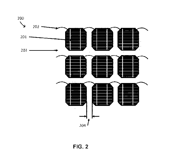
[0021] FIG. 2 is a conceptual diagram illustrating an example flexible MCSC
assembly in accordance with some examples of the disclosure. As described
below, the MCSC assembly may include an array of SCC units affixed to a
CA 03067373 2019-12-13
WO 2018/232324
PCT/US2018/037884
substrate with spaces between adjacent SCC units, where the SCC units are
electrically interconnected to form an electrical circuit.
[0022] FIG. 3 is a conceptual diagram illustrating another example MCSC
including an array of SCCs affixed to a substrate with spaces between adjacent
SCC units. As described below, the SCC units are electrically interconnected
to
form an electrical circuit. The substrate may be a lattice or scaffold
comprised of a
frame surrounding support rods or bars. The space between adjacent SCC units
determines the effective porosity of the MCSC assembly.
[0023] FIGS. 4a and 4b are conceptual diagrams illustrating another example
MCSC including an array of SCCs affixed to a substrate with spaces between
adjacent SCC units. In the example, the substrate is a mesh or net. As
described
below, the space between adjacent SCC units determines the effective porosity
of
the MCSC assembly. The mesh or net is advantageous as it allows the spaces to
be
adjusted without changing the substrate mesh or net structure.
[0024] FIGS. 5a, 5b, and 5c are conceptual diagrams illustrating how the frame
and
support members of an MCSC assembly can be combined with SCC base layer
encapsulant with top layer transparent encapsulants used to complete the
encapsulation of the individual SCC units.
DETAILED DESCRIPTION
[0025] In some instances, silicon wafer solar panels are generally large with
dimensions measured in meters and are constructed as follows from bottom (side
away from sunlight) to top. At the bottom is a backsheet layer commonly of a
material such as a polyvinyl fluoride film. A specific example of such a film
is
TEDLAR which is produced by the E. I. du Pont de Nemours and Company or its
affiliates.
[0026] The backsheet needs to be durable to weathering, prevent penetration by
water, be lightweight, and be able to reflect light off its top surface. The
next layer
is commonly an encapsulating material such as EVA, ethyl vinyl acetate, that
both
seals the panel against the elements, and serves as a lubricating layer that
allows
materials adjacent to one another with different coefficients of thermal
expansion to
slide against one another during temperature changes. Next comes an array of
6
CA 03067373 2019-12-13
WO 2018/232324
PCT/US2018/037884
silicon wafers. The wafers are generally arranged in periodic arrays that
allow
wafers to be strung together with electrically conducting tabbing material to
make
the requisite electrical circuits to deliver specified voltage and currents
from the
panel. The wafers are arranged to maximize the areal coverage of the panel
surface
by wafers thus generating the most electrical power for given surface area.
The
wafers are covered by another layer of EVA. The top of the panel is most often
glass, nominally 4 mm thick. The glass provides the overall strength of the
module
in addition to permitting sunlight to impinge on the silicon wafer solar
cells. This
entire stacked assembly is surrounded by an aluminum frame and all interfaces
of
the layers are sealed with various sealers and tapes to isolate the interior
of the
panel from the environment.
[0027] The resultant panel is large, heavy, rigid, and does not allow
sunlight, air, or
water to pass through the panel.
[0028] These characteristics of traditional silicon wafer solar panels
strongly
constrain where they can be installed, force large costs to be incurred in
their
support structures, and damage the environment.
[0029] The specific problems addressed by some examples of the disclosure are
rigidity that prevents solar panels from conforming to surfaces with
curvature,
excessive weight and wind loading (no air passage through panel) that require
major changes to building structures for roof installed solar panels, and
damage to
local eco systems where solar panels are installed.
[0030] In some embodiments, the disclosure relates to solar cell assemblies of
various types that are sufficiently flexible to conform to surfaces and are
stable to
environmental conditions of humidity, temperature, and UV radiation.
[0031] An example solar cell assembly may consist, consist essentially of, or
comprise a plurality of self-contained solar cell capsules, SCC, affixed to a
flexible
substrate, with SCCs separated from one another by a prescribed distance
maintained by the attachment of the SCCs to the flexible substrate, and the
SCCs
interconnected to one another by a network of electrical conductors. A self-
contained solar cell unit that converts light to electricity is called a Solar
Cell Unit,
SCU. To protect SCUs from environmental conditions such as humidity and
oxygen, the individual SCUs may be encapsulated by materials that are
impervious
7
CA 03067373 2019-12-13
WO 2018/232324
PCT/US2018/037884
to water, oxygen and other contaminants yet permit the entry of light on at
least one
surface to energize the SCU and produce electricity. Such an encapsulating
material
may be referred to herein as a Transparent Protective Material (TPM). An SCU
totally encapsulated by TPM may be referred to herein as a Solar Cell Capsule
(SCC). The full assembly of SCUs interconnected together in an electrically
parallel
fashion may be referred to herein as a Massively Connected Solar Cell (MCSC).
[0032] An example of a single SCC unit in accordance with the disclosure is
shown
in FIGS. la and lb. FIG. la is a conceptual diagram illustrating a side view
of the
SCC 100 and FIG. lb is a conceptual diagram illustrating a top-down view of
the
SCC 100. In this example, the SCC 100 includes of a silicon wafer 101 totally
encapsulated in a suitable material 103. The silicon wafer 101 constitutes the
SCU
of the SCC unit. Electrically conducting tabbing material 102 is electrically
coupled to silicon wafer and may define an anode and cathode, e.g., on either
side,
for the silicon wafer SCU. Electrically conducting tabbing material 102 is
shown to
project to the exterior of the SCC 100 through encapsulating material 103 thus
permitting the anode and cathode to be connected to other SCC units in the
overall
MCSC ensemble.
[0033] The encapsulating material 103 may be any suitable material that will
isolate
the wafer 101 from materials or conditions that may harm the wafer 101. One
choice of the encapsulating material is an undiluted clear difunctional
bisphenol
A/epichlorohydrin derived liquid epoxy resin cross-linked or hardened with an
aliphatic amine hardener. Such a hardener will prevent deterioration of the
epoxy
when it is exposed to UV radiation. The choice of such an epoxy as the
encapsulant
is not limiting and any material suitable to the application can be used. For
example,
the encapsulant may be chosen as a silicone rubber that has been prepared by a
platinum catalyst synthetic route to avoid acetic acid contaminants that would
corrode the encapsulated electrical connections. The encapsulant may also
include
more than one layer. In the case of the silicone rubber encapsulant one may
sandwich the SCC inside layers of ETFE or PTFE film that are heat sealed to
isolate
the SCC from the environment. Such a structure may provide a self-cleaning
action
to atmospheric pollutants such as soot and pollens since the ETFE and PTFE are
known to be strongly hydrophobic so water cannot wet them.
8
CA 03067373 2019-12-13
WO 2018/232324
PCT/US2018/037884
[0034] Any suitable technique may be used to form the example SCC of FIGS. la
and lb. One example technique to prepare the SCC 100 using the aforementioned
epoxy material is to solder tabbing material to a silicon wafer to form the
electrodes
102, prepare a mold from a material such as silicone rubber that the epoxy
will not
wet, then fill the mold with the epoxy material 103, insert the wafer 101 and
electrodes 102 into the epoxy material 103 is such a manner to eliminate or
substantially eliminate bubbles, and then cure the epoxy material 103. Since
the
epoxy does not wet the silicone rubber mold, the completed SCC can be easily
removed from the mold once the epoxy has cured.
[0035] As described herein, in some examples, a plurality of individual SCCs
(e.g.,
like SCC 100 shown in FIGS la and lb) may be attached to a substrate and
electrically interconnected to form a MCSS. Any suitable substrate may be
employed in such a MCSS. In some examples, the flexible substrate may be a
flexible fabric substrate. The fabric substrate may be a knitted, woven,
needled,
felt, and/or non-woven fabric. The flexible substrate may be a single layer or
multiple layer construction with the composition of each layer being the same
or
different than the composition of other layers. Each layer may be composed of
a
single component or be composed of multiple materials the proportion of each
material to the others being determined by the ultimate purpose of the overall
solar
cell assembly. Flexible substrate layers may be bonded to one another,
laminated
to one another or integrally woven, knitted, felted, or needled together to
form the
flexible substrate.
[0036] In some examples, the flexible substrate may be a flexible film
substrate.
The flexible substrate may be a single layer or multiple layer construction
with the
composition of each layer being the same or different than the composition of
other
layers. Each layer may be composed of a single component or be composed of
multiple materials the proportion of each material to the others being
determined
by the ultimate purpose of the overall solar cell assembly. Flexible substrate
layers
may be bonded to one another, laminated to one another to form the flexible
substrate.
[0037] In some examples, the flexible substrate may be a flexible mesh
substrate.
The flexible substrate may be a single layer or multiple layer construction
with the
9
CA 03067373 2019-12-13
WO 2018/232324
PCT/US2018/037884
composition of each layer being the same or different than the composition of
other
layers. Each layer may be composed of a single component or be composed of
multiple materials the proportion of each material to the others being
determined
by the ultimate purpose of the overall solar cell assembly. Flexible substrate
layers
may be bonded to one another, laminated to one another or integrally woven,
knitted, felted, or needled together to form the flexible substrate. It is
anticipated
that a flexible mesh substrate may serve as the electrical conduction network
of the
MCSC for either the anode or the cathode. A two-layer mesh with the layers
insulated from one another may serve as the electrical conduction networks for
both the anode and the cathode.
[0038] In some examples, the flexible substrate may be a flexible net
substrate.
The difference between a mesh and a net is that in a mesh, points of overlap
of two
fibers are bonded to one another (though not necessarily all points of overlap
are
bonded) whereas in a net, points of overlap of two fibers are knotted in some
fashion (though not necessarily all points of overlap are knotted) the knots
may
allow points of overlap to be either tight or loose. The flexible substrate
may be a
single layer or multiple layer construction with the composition of each layer
being
the same or different than the composition of other layers. Each layer may be
composed of a single component or be composed of multiple materials the
proportion of each material to the others being determined by the ultimate
purpose
of the overall solar cell assembly. Flexible substrate layers may be bonded to
one
another, laminated to one another or integrally woven, knitted, felted, or
needled
together to form the flexible substrate. It is anticipated that a flexible
mesh
substrate may serve as the electrical conduction network of the MCSC for
either
the anode or the cathode. A two-layer mesh with the layers insulated from one
another may serve as the electrical conduction networks for both the anode and
the
cathode.
[0039] In the cases of the flexible substrate being a fabric, a net, or a
mesh, it is
anticipated that the fibers or other fabric, net or mesh material in the
flexible
substrate may themselves be electrical conductors; one set of fibers being the
electrical conducting network for the cathode and another set the electrical
conducting network for the anode. It is anticipated that the individual
conducting
CA 03067373 2019-12-13
WO 2018/232324
PCT/US2018/037884
fibers be extensible such as using iStretch wires from Minnesota Wire, 1835
Energy Park Dr., St Paul, MN 55108. In such a case that is intended to be
exemplary and not limiting, the individual conducting fibers would have the
full
electrical conductivity of copper wire but is extensible to 30% of its length
between attachment points to SCCs.
[0040] As described herein, an array of individual SCCs may be attached to the
flexible substrate. The substrate serves to maintain the relative positions of
SCCs
one to another consistent with the mechanical properties of the substrate. The
SCCs are attached to the substrate by any of several means. The means
described
in this disclosure are intended to be exemplary and are not intended to be
limiting
in any way.
[0041] In the case of the substrate being a fabric or a film, an SCC may be
attached
to the substrate by an adhesive such as an epoxy, a silicon rubber, a
polyurethane.
The specific adhesive choices illustrated by epoxy, silicon rubber, or
polyurethane
are not limiting and any adhesive suitable for a final implementation is
envisaged
by the invention. In such cases the SCC may be a completely assembled and
functioning solar cell requiring only to be attached to the substrate and/or
to
establish the overall MCSC structure by being connected to other SCCs in the
MCSC by the conducting network that would establish the parallel electrical
circuit. Alternatively, the SCC may be in a partial state of completed
assembly
with its final assembly completed after or during the attachment of the SCC to
the
substrate and/or to the conducting network.
[0042] In the special cases of the substrate being a woven or unwoven fabric,
a net,
or a mesh, the SCC may be made of an appropriate material such as a polymer
resin that the SCC is caused to partially penetrate the substrate thereby
sterically
interlocking the SCC to the substrate. In this manner, an exceptionally strong
bond
between the SCC and the substrate is formed that maintains mechanical
integrity
throughout bending and stretching motions and stresses. It is further
envisaged, but
not in limiting fashion, that the adhesive, resin, or other such material may
be part
of the SCC structure itself and that such attachment of the SCC to the
substrate
may be performed prior to the final assembly of the SCC or the SCU contained
therein.
11
CA 03067373 2019-12-13
WO 2018/232324
PCT/US2018/037884
[0043] In the special cases of the substrate being a net or mesh of conductive
fibers
that will itself form the conducting electrical network, both a mechanical
connection and one or more electrical connections must be made between the SCC
and the substrate. The SCC has both a cathode and an anode. The cathode and
anode of each SCC must be electrically connected to the cathodes and anodes of
other SCCs in the manner that delivers the electrical voltage and amperage
required by the assembly in its end use. Other electrical components such as
diodes
are also included in the circuit as required by the end application. The
electrical
connections may be solder, wire bonds, conductive adhesives or any other type
of
electrical connection suitable to the applications of the final assembly.
[0044] In instances where such electrical connections may not be tolerant of
stresses associated with bending or stretching motions caused by flexing of
the
overall MCSC, stress relief structures in addition to the electrical
connections may
also need to be provided. In such cases, it is envisaged that the attachment
of the
SCC to the substrate will involve, but not be limited to, adhesives or resins
that
penetrate or partially penetrate the mesh or net. It is further envisaged, but
not in
limiting fashion, that the adhesive, resin, or other such material may be part
of the
SCC structure itself and that such attachment of the SCC to the substrate may
be
performed prior to the final assembly of the SCC or the SCU contained therein.
[0045] The SCU that is contained within the SCC that, in turn, is attached to
the
substrate and networked both mechanically and electrically to other SCCs to
form
the MCSC may be, but is not limited to, a silicon wafer, a perovskite solar
cell, or
any other suitable solar cell construction compatible to the overall
specification for
the MCSC assembly. For example, in the SCC 100 of FIGS. la and lb, silicon
wafer 101 constitutes a SCU. The SCCs in the MCSC need not all be identical to
one another. They may differ in size, shape, and in the type of SCU contained
therein in any combination suitable for the final application of the MCSC.
Each
SCC is not limited to containing only a single type SCU within the
encapsulation.
Hybrid SCU constructions involving, for example, perovskite and silicon wafer
SCU components are known. The disclosure is not limited to just the
combination
of perovskite and silicon wafer hybrid structure.
12
CA 03067373 2019-12-13
WO 2018/232324
PCT/US2018/037884
[0046] To ensure long-term function and reliability, an SCU within an SCC
should
be protected from environmental elements such as humidity and oxygen and be
protected from UV radiation while still being exposed to visible radiation.
Indeed,
the major issues that prevent perovskite solar cells from being commercially
viable
are their stabilities against humidity, oxygen and UV radiation and
temperature.
One such means of encapsulation is shown in FIGS. la and lb. Example MCSC of
the disclosure may solve some or all four of these problems.
[0047] FIG. 2 is a conceptual diagram illustrating an example flexible MCSC
assembly 200 in accordance with some examples of the disclosure. As shown in
FIG. 2, flexible MCSC assembly 200 includes a plurality of SCCs 201 (only one
SCC is labelled for clarity). SCCs 201 may be the same or similar to that
shown
and described as SCC 100 in FIGS. la and lb. For example, SCCs 201 may
include are silicon wafers individually encapsulated by a polymeric resin that
isolates the silicon wafer from the environment but permits electrical
conductors
202 to extend from the anode and the cathode of the silicon wafer of SCC 201
to
outside the encapsulating material (e.g., material 103 of FIGS. la and lb).
Each
silicon wafer SCC 201 may be attached to a flexible substrate 203 by a
suitable
adhesive or other appropriate attachment mechanism such as staples, rivets, or
loops, with sufficient space 204 between adjacent individual SCC units 201 to
permit the MCSC assembly 200 to conform to a planar or non-planar surface upon
which assembly 200 is placed. For 6 inch, square, SCC units, an example space
is
about 0.5 inch to 1 inch to give the overall MCSC unit an overall empty space
or
porosity of between 0.1 and 0.3. Such a spacing will dramatically reduce wind
loading effects on MCSC panels with the 0.3 porosity giving a much greater
reduction in wind loading than a spacing of 0.1. The wind pressure loss
coefficient
decreases with the inverse square of the porosity. A space of about 2 inches
or
more on such 6 inch, square SCC units, allows the MCSC assembly to be folded
over upon itself if the SCC units are mounted on a flexible substrate 203.
[0048] The specific examples of the attachment mechanisms described herein are
not limiting as any attachment required by the end use of the MSCS 200 is
envisaged by the disclosure. In some cases, the spaces 204 between individual
SCCs 201 may be sufficiently large to permit the folding of individual SCCs
201
13
CA 03067373 2019-12-13
WO 2018/232324
PCT/US2018/037884
over one another. Spaces 204 in the two dimensions need not be the same nor
uniform throughout the MCSC assembly 200. Such an assembly will conform to
surfaces with curvature limited by the dimension of the SCC. Typical sizes of
such
SCC using commercially available silicon wafers are about five to about six
inches
and are roughly square, but the disclosure is not limited to these specific
dimensions. The polymeric resin may be an epoxy such as EPON 828 combined
with an aliphatic amine hardener that renders the resultant epoxy encapsulant
resistant to UV degradation. EPON is a trademark of Hexion Inc., Columbus,
Ohio. Such epoxy resins are well-known to be resistant to penetration by
oxygen,
water, acids and bases and exhibit good weathering characteristics. The choice
of
such an epoxy is exemplary only and is not limiting. Other choices of
encapsulating structures are envisaged such as the use of PTFE or ETFE films
either alone or in combination with platinum catalyst silicone rubbers. The
advantage of such encapsulating materials over EVA that is used in other
silicon
wafer solar panels is that no acetic acid is formed in the case of some amount
of
UV degradation. The acetic acid, even in trace amounts, corrodes electrical
connections to the silicon wafer. The electrical conductors from the SCC
cathode
and anode are electrically insulated from one another and connected to
conductors
from other SCC units in the MCSC assembly to form an electrical circuit
appropriate to the amperage and voltage that is expected to be drawn from the
overall MCSC assembly. The electrical power drawn from the MCSC assembly
can be used to power equipment, instruments, heaters, or other electrical
device in
the vicinity of the MCSC; can be stored in a battery or fuel cell for use when
the
sun does not shine or when the power from the MCSC is not optimum for an
intended purpose; or can be delivered to an electrical power grid.
[0049] A second, preferred embodiment based on the example assembly 200
shown in FIG. 2 is to use as a flexible substrate 203 a suitable SUPERFABRIC ,
a
product of Higher Dimension Materials, Oakdale, Minnesota, USA, as the
flexible
substrate 203. SUPERFABRIC is an abrasion resistant, cut resistant, stain
resistant fabric that gives the resultant flexible MCSC considerable
durability in
and of its own right while preserving desired flexibility. The choice of
SUPERFABRIC as a flexible substrate is not limiting. Any substrate material
14
CA 03067373 2019-12-13
WO 2018/232324
PCT/US2018/037884
including woven or non-woven fabrics, nets, screens, or meshes of suitable
materials may be used instead of, or in addition to, one another or to
SUPERFABRIC . The flexible substrate may be a single layer or be multiple
layers depending on the requirements of the final application.
[0050] A specific example of use for the preferred embodiment (or other
embodiment described herein) is as a roofing material. In this instance, the
choice
of SUPERFABRIC as the flexible substrate 203 would be chosen to be
waterproof so that the MCSC assembly may serve the dual function of shingles
and
as solar electricity generation. The SUPERFABRIC substrate material is
abrasion
resistant and sufficiently durable to permit workers to walk on the
SUPERFABRIC substrate 203 without damaging it. SUPERFABRIC is stain
resistant so the roofing material will maintain its color and aesthetic appeal
for
many years even though exposed to weather and pollutants. The SCC units 201 in
such a roofing application may use, but is not limited to, an epoxy resin such
as
EPON 828 combined with an aliphatic amine hardener that renders the resultant
epoxy encapsulant resistant to UV degradation. Such encapsulations can be made
sufficiently strong and robust to withstand workers walking on them or moving
equipment over them without damaging the SCC unit. Major advantages of using
the preferred embodiment as a roofing material over and against traditional
solar
modules that are mounted on roofs are that the MCSC assembly 200 may be
lighter
in weight and, since the MCSC is mounted flush to the roof, subjects the roof
to
much less wind loading. Traditional solar panels mounted on roofs often
require
major structural changes to the roof to support the weight and the wind
loading. In
many regions such roof installations must withstand the wind load of a 100
mile
per hour wind.
[0051] FIG. 3 is a conceptual diagram illustrating another example MCSC
assembly 300 in accordance with some examples of the disclosure. As
illustrated
in FIG. 3, the MCSC assembly 300 includes SCCs 301, e.g., as described in
FIGS.
la and lb as SCC 100, which may be silicon wafers individually encapsulated by
a
polymeric resin that isolates the silicon wafer from the environment but
permits
electrical conductors 302 to extend from the anode and the cathode of the
silicon
wafer to outside the encapsulating material. Each silicon wafer SCC 301 is
CA 03067373 2019-12-13
WO 2018/232324
PCT/US2018/037884
attached to a substrate that is a porous frame, lattice, or scaffold. FIG. 3
shows a
lattice or scaffold constructed of support bars or rods 303 connected to a
circumferential frame 304 by a suitable adhesive or other appropriate
attachment
mechanism such as staples, rivets, or loops, with sufficient space 305 between
adjacent individual SCC units 301 to permit the MCSC assembly 300 to permit
air
and sunlight to pass through the MCSC assembly 300. The specific examples of
the attachment mechanisms are not limiting as any attachment required by the
end
use of the MSCS is envisaged by the disclosure. The disclosure envisages that
the
materials used to form the scaffold, frame, or lattice may be the same or
different
than other materials used in the frame, scaffold, or lattice. The disclosure
also
envisages that the frame, scaffold, and lattice elements may by themselves or
in
concert with one another establish the electrical circuit required by the end
application of the MCSC.
[0052] In some examples, there are many advantages of the embodiment of the
disclosure shown in FIG. 3 over and against traditional silicon wafer solar
cells.
[0053] For example, the lattice or scaffold structure 300 may permit a rigid
panel
with dramatically reduced weight and wind loading. Since air passes unimpeded
through the spaces between the SCC units 301, wind loading is dramatically
reduced. The spaces 305 form a porosity for the overall panel. Porosity is the
fractional area of the panel that does not obstruct sunlight or air passage.
Even a
small amount of porosity strongly affects the wind load. Studies on the wind
load
of porous panels dates from the second world war when radar antennae were
first
being installed to the present day for porous structures that can be used as
animal
shelters that provide animals with shade while still providing ventilation.
Such
structures are especially useful in geographies such as Australia where
livestock is
commonly located many miles from ordinary farm structures. Those studies show
that the wind load factor decreases with the square of the porosity. The
example of
FIG. 3 may allow such structures to produce their own local electricity. That
electricity can be used to aid ventilation or to power transceivers that relay
animal
health metrics back to a farmstead. Livestock animals commonly have embedded
sensors that monitor temperature, blood oxygen, dehydration, and a number of
other health factors. That information is generally transmitted by RFID or
similar
16
CA 03067373 2019-12-13
WO 2018/232324
PCT/US2018/037884
technologies to a receiver that is local to the animals. That receiver needs
to
transmit the data to the farmstead many miles away and that requires
substantial
power. That power can be conveniently provided by the example of FIG. 3 by
incorporating solar energy collection into the porous structure that is
otherwise
used to shelter the animals. The porosity retains the shading, ventilation,
and
reduced wind loading required by such structures while at the same time allows
local solar electricity generation.
[0054] Another advantage of the porous structure 300 of the third example is
that it
may allow air cooling of the individual SCC units 301. Heat is an enemy of
silicon
wafer solar cells and electrical generation efficiency declines dramatically
with
increasing temperature. The porous structure 300 permits cooling of the SCC
units
as air is allowed to completely surround and flow between the SCC units.
[0055] Another advantage of the porous structure 300 of the third example is
that it
may allow sunlight and rain to penetrate through the panel to the surface
beneath it.
The land beneath traditional solar farms may be an environmental wasteland.
Nothing useful can grow under the panels because little sunlight or moisture
reaches the ground beneath. The shade, however, can foster the growth of
harmful
molds that are foreign to the regions of the solar farms. Such molds have no
natural
enemies in those regions and are not controlled by natural means.
[0056] The specific example of a frame with a lattice or scaffold structure to
produce a panel with porosity is not limiting. The disclosure envisages that
the
MCSC assembly be mounted on a porous screen or porous mesh with the desired
degree of porosity for air, sunlight, and moisture passage. Such structures
can also
be flexible thereby enabling such structures as animal shelters to be tent-
like
greatly increasing the convenience of setting up and moving such structures.
[0057] Examples of the MCSC 400 mounted on a mesh, screen or net are shown in
FIGS. 4a and 4b. In FIGS. 4a and 4b, the individual SCC units 401 are affixed
to a
screen, mesh, or net 402 which is supported by a frame 403. The spaces 404 on
such a screen, mesh, or net type of substrate are infinitely adjustable to
deliver the
porosity required in a final application.
[0058] In the MCSC 400 the material of the mesh, screen, or net can be any
suitable material such as a yarn, or fiber that can be either a natural
substance such
17
CA 03067373 2019-12-13
WO 2018/232324
PCT/US2018/037884
as cotton or wool or a man-made material such as nylon, polyester, or Kevlar.
The
choice of material for the yarn or fiber is not limiting. In other instances,
the mesh,
net, or screen may be made from a metal such as aluminum, titanium, stainless
steel, or an advanced composite such as carbon fiber. The specific choice of
material for the screen, net or mesh is not limiting as any choice of material
suitable for the final application is envisaged by the disclosure. The frame
material
may be aluminum, stainless steel, titanium, carbon fiber or any other material
suitable for the construction of the frame. The choice of a specific material
for the
frame is not limiting. The space 404 shown in FIG. 4a gives a porosity of
approximately 0.3. The porosity in the example of FIG. 4b, which is
illustrated in
size relative to FIG. 4b, is substantially smaller. The choice of spacing is
not
limiting and is made on the basis of wind loading that is expected in the
final
implementation of the MCSC assembly.
[0059] As mentioned in reference to the SCC 100 shown in FIG. 1, the
encapsulant
may be comprised of more than a single layer and such layers need not
necessarily
be of the same composition as one another. This freedom allows another
preferred
embodiment of the disclosure. FIG. 5a is a conceptual diagram illustrating an
example MCSC unit 500 wherein the bottom portion of the encapsulant of the SCC
501 is incorporated with a frame and support members as a single unit 502. For
example, the bottom portion of the encapsulant may be integrally formed with
the
frame and support member portion (e.g., as single piece). The spaces 503
between
adjacent bottom portions of the encapsulant and between the bottom portions of
the
encapsulant and the perimeter frame are open spaces (porosity) that allow air,
moisture, and sunlight to flow between and around the individual units in the
MCSC 500. In this way, a strong, lightweight single component structure can
provide both support for the overall MCSC assembly and provide the base for
the
encapsulation of the individual SCUs. Typical materials for the frame, support
members and bottom layer of encapsulant is an epoxy, epoxy composite,
fiberglass
composite, or carbon fiber. The disclosure envisages that other materials may
also
be used so the choices of epoxy, epoxy composite, fiberglass composite, or
carbon
fiber are not limiting. The choice of materials for the frame, the support
members,
18
CA 03067373 2019-12-13
WO 2018/232324
PCT/US2018/037884
and the bottom layer of the encapsulant may be the same as one another or may
be
different.
[0060] FIG. 5b is a conceptual diagram illustrating the single unit 502 of
FIG. 5a
with SCU units installed on the encapsulant bases of the SCC. The illustration
shows silicon wafers 504 as the choice for the SCU, but the invention is not
limited
by this choice. SCU comprised of perovskite materials, CdTe materials, or CIGS
materials or other solar cell materials may also be used.
[0061] FIG. 5c is a conceptual diagram illustrating the single unit 502 of
FIG. 5b
with a top layer transparent encapsulant 505 applied over the individual SCU
units
located on the encapsulant bases. This top layer must be transparent to
visible light
to permit sunlight to impinge on the SCU contained within the encapsulant. The
transparent encapsulant 505 may itself be a layered structure. Typical
materials for
the transparent encapsulant 505 include epoxy, ETFE film, or PTFE film, but
the
invention is not limited by these specific choices of materials as other
materials
may also prove beneficial. Examples of layered structures for the transparent
encapsulant 505 include but are not limited to silicon rubber covered by
epoxy,
silicon rubber covered by ETFE fil, or silicon rubber covered by PTFE film.
[0062] As illustrated in FIGS. 5a-5c, the bottom portion of the encapsulant
may be
integrally formed with the frame and support member portion (e.g., as single
piece)
rather than requiring SCCs that have been pre-formed and subsequently attached
to
the frame and support members. The individual SCU units may be placed on the
bottom portion of the encapsulant (e.g., as shown in FIG. 5b) and then
encapsulated on top and sides (e.g., as shown in FIG. Sc).
[0063] Regardless of the means of providing porosity in such a panel, whether
it
be by mounting a MCSC assembly on a frame, scaffold, lattice, mesh, or screen,
or
incorporating porosity as spaces in a unified structure that provides both
structural
support and a base for encapsulants, the disclosure envisages providing a
porosity
in the 0.2 to 0.4 range, though such a range is not limiting. A greater or
lesser
porosity may be desired for a specific application. A traditional solar panel
has
essentially no porosity. An increase in porosity from 0.1 to 0.4 would reduce
the
wind pressure loss coefficient by a factor of 16. Using porous MCSC assemblies
19
CA 03067373 2019-12-13
WO 2018/232324
PCT/US2018/037884
on structures subjected to strong winds can dramatically improve the
durability of
such structures while still producing the requisite amount of electricity.
[0064] Various examples have been described. These and other examples are
within the scope of the following claims.