Note : Les descriptions sont présentées dans la langue officielle dans laquelle elles ont été soumises.
TWO-FILTER LIGHT DETECTION DEVICES AND
METHODS RELATED TO SAME
[0001] <Blank>
BACKGROUND
[0001] Various protocols in biological or chemical research involve performing
a large number
of controlled reactions on local support surfaces or within predefined
reaction chambers. The
designated reactions may then be observed or detected and subsequent analysis
may help identify
or reveal properties of chemicals involved in the reaction. For example, in
some multiplex
assays, an unknown analyte having an identifiable label (e.g., fluorescent
label) may be exposed
to thousands of known probes under controlled conditions. Each known probe may
be deposited
into a corresponding well of a microplate. Observing any chemical reactions
that occur between
the known probes and the unknown analyte within the wells may help identify or
reveal
properties of the analyte. Other examples of such protocols include known DNA
sequencing
processes, such as sequencing-by-synthesis (SBS) or cyclic-array sequencing.
[0002] In some conventional fluorescent-detection protocols, an optical system
is used to direct
an excitation light onto fluorescently-labeled analytes and to also detect the
fluorescent signals
that may emit from the analytes. However, such optical systems can be
relatively expensive and
involve a relatively large benchtop footprint. For example, such optical
systems may include an
arrangement of lenses, filters, and light sources.
[0003] In other proposed detection systems, the controlled reactions occur on
local support
surfaces or within predefined reaction chambers provided over an electronic
solid-state light
detector or imager (e.g., a complementary metal-oxide-semiconductor (CMOS)
detector or a
charged-coupled device (CCD) detector) that does not involve a large optical
assembly to detect
the fluorescent emissions. However, such proposed solid-state imaging systems
may have some
1
Date Recue/Date Received 2021-05-13
CA 03067424 2019-11-29
WO 2019/125690 PCT/US2018/062019
limitations. For example, fluidically delivering reagents (e.g., fluorescently-
labeled molecules)
to the analytes that are located on the electronic device of such systems may
present challenges.
In some scenarios, the reagent solution may breach the electronic device and
corrode
components thereof, for example.
BRIEF DESCRIPTION
[0004] In one aspect of the present disclosure, a device is provided. The
device comprises a
reaction structure to contain a reaction solution and a plurality of reaction
sites that generate light
emissions in response to incident excitation light after treatment with the
reaction solution. The
reaction solution may initiate a reaction and/or form a reaction product at
the reaction sites that
generate the light emissions in response to the excitation light. The reaction
structure is
positioned over a device base of the device The device also comprises a
plurality of light
sensors within the device base, and device circuitry within the device base
electrically coupled to
the plurality of light sensors and configured to transmit data signals based
on photons detected
by the light sensors. The device further comprises a plurality of light guides
with input regions
to receive the excitation light and the light emissions from at least one
corresponding reaction
site, the light guides extending into the device base from the input regions
toward at least one
corresponding light sensor. Each of the plurality of light guides comprises a
first filter region
formed of a first filter material to filter the excitation light of at least a
first wavelength and
permit the light emissions of a second wavelength to pass therethrough to the
at least one
corresponding light sensor, and a second filter region formed of a second
filter material to filter
the excitation light of at least the first wavelength and permit the light
emissions of a third
wavelength to pass therethrough to the at least one corresponding light
sensor.
[0005] In some examples, at least one first reaction site of the plurality of
reaction sites emits
light of at least the second and third wavelengths in response to excitation
light of the first
wavelength after treatment with the reaction solution (e.g., after the
reaction solution has
initiated reactions and/or formed at least one reaction product at the
reaction sites). In some
examples, at least one first reaction site of the plurality of reaction sites
emits light of at least the
second and third wavelengths in response to excitation light of the first
wavelength and a fourth
wavelength, respectively, after treatment with the reaction solution. In some
examples, at least
one first reaction site of the plurality of reaction sites emits light
emissions of the second
wavelength in response to excitation light of the first wavelength after
treatment with the
2
CA 03067424 2019-11-29
WO 2019/125690 PCT/US2018/062019
reaction solution, and at least one second reaction site of the plurality of
reaction sites emits light
emissions of the third wavelength in in response to excitation light of a
fourth wavelength after
treatment with the reaction solution.
[0006] In some examples, the device further comprises a support layer within a
bottom portion
of the light guides extending below and about a bottom portion of the first
regions. In some such
examples, the support layer is comprised of an oxide, a nitride, or a
combination thereof. In
other such examples, the second region of the light guides extends over the
support layer and
about the first regions. In some such examples, the first and second regions
of the light guides
form the input regions of the light guides.
[0007] In some examples, the device further comprises a second liner layer
that is positioned
between the support layer and the device circuitry at the bottom portion of
the light guides, and
that is positioned between second filter region device circuitry within a top
portion of the light
guides. In some such examples, the second liner layer comprised a silicon
nitride shield layer.
In some examples, the device circuitry of the device base forms complementary
metal-oxide
semiconductor (CMOS) circuits.
[0008] In some examples, the first filter material further filters the light
emissions of the third
wavelength, and the second filter material further filters the light emissions
of the second
wavelength. In some examples, the first filter material is a polymer material
with a first dye, and
the second filter material is a polymer material with a second dye that
differs from the first dye.
In some examples, each of the plurality of reaction sites are immobilized to
the reaction structure
within at least one reaction recess of the reaction structure.
[0009] In some examples, the reaction solution initiates a reaction and/or
forms a reaction
product at the reaction sites that generates the light emissions of the second
and third
wavelengths in response to the incident excitation light. In some such
examples, the at least one
reaction site comprises at least one analyte, and the reaction solution
comprises an aqueous
solution containing at least one fluorescently-labeled molecule. In some such
examples, the at
least one analyte comprises an oligonucleotide, and the at least one
fluorescently-labeled
molecule comprises a fluorescently-labeled nucleotide.
[0010] In another aspect of the present disclosure, a biosensor is provided.
The biosensor
comprises any of the devices described above. The biosensor also comprises a
flow cell
mounted to the device, and the reaction sites contained on the reaction
structure. The flow cell
3
CA 03067424 2019-11-29
WO 2019/125690 PCT/US2018/062019
comprises the reaction solution and at least one flow channel that is in fluid
communication with
the reaction sites of the reaction structure to direct the reaction solution
thereto.
[0011] In another aspect of the present disclosure, a method is provided. The
method comprises
forming a plurality of trenches within a device base comprising a plurality of
light sensors and
device circuitry electrically coupled to the light sensors configured to
transmit data signals based
on photons detected by the light sensors. The plurality of trenches each
extend from a top
surface of the device base and toward at least one corresponding light sensor.
The method also
comprises depositing a support layer over inner surfaces of the plurality of
trenches. The method
further comprises filling the plurality of trenches over the deposited support
layer with a first
filter material that filters light of at least a first wavelength and permits
light of a second
wavelength to pass therethrough to the at least one corresponding light
sensor. The method also
comprises removing an upper portion of the deposited support layer within the
plurality of
trenches positioned between the device base and the first filter material to
form a plurality of
voids. The method further comprises filling the plurality of voids with a
second filter material
that filters light of at least the first wavelength and permits light of a
third wavelength to pass
therethrough to the at least one corresponding light sensor to form a
plurality of light guides.
The method also comprises forming a reaction structure over the device base
and the plurality of
light guides for containing a reaction solution and at least one reaction site
that generates light of
at least one of the second and third wavelengths after treatment with the
reaction solution in
response to incident excitation light of at least the first wavelength.
[0012] In some examples, at least one first reaction site emits light of at
least the second and
third wavelengths in response to excitation light of the first wavelength
after treatment with the
reaction solution (e.g., after the reaction solution has initiated reactions
and/or formed at least
one reaction product at the reaction sites). In some examples, at least one
first reaction site emits
light of at least the second and third wavelengths in response to excitation
light of the first
wavelength and a fourth wavelength, respectively, after treatment with the
reaction solution In
some examples, at least one first reaction site emits light emissions of the
second wavelength in
response to excitation light of the first wavelength after treatment with the
reaction solution, and
at least one second reaction site emits light emissions of the third
wavelength in in response to
excitation light of a fourth wavelength after treatment with the reaction
solution.
4
CA 03067424 2019-11-29
WO 2019/125690 PCT/1JS2018/062019
[0013] In some examples, removing the upper portion of the deposited support
layer within the
plurality of trenches forms a support layer portion that extends below and
about a bottom portion
of the first regions. In some examples, the method further comprises
depositing a second liner
layer over the inner surfaces of the plurality of trenches and over the top
surface of the device
base prior to depositing the support layer such that the support layer extends
over the second
liner layer. In some examples, the first filter material further filters the
light of the second
wavelength, and the second filter material further filters the light of the
first wavelength. In
some examples, the first filter material comprises a polymer material with a
first dye, and the
second filter material comprises a polymer material with a second dye that
differs from the first
dye.
[0014] It should be appreciated that all combinations of the foregoing aspects
and additional
concepts discussed in greater detail below (provided such concepts are not
mutually inconsistent)
are contemplated as being part of the inventive subject matter disclosed
herein.
[0015] These and other objects, features and advantages of this disclosure
will become apparent
from the following detailed description of the various aspects of the
disclosure taken in
conjunction with the accompanying drawings.
DRAWINGS
[0016] These and other features, aspects, and advantages of the present
invention will become
better understood when the following detailed description is read with
reference to the
accompanying drawings, which are not necessarily drawn to scale and in which
like reference
numerals represent like aspects throughout the drawings, wherein:
[0017] FIG. 1 illustrates, in one example, a cross-section of a biosensor in
accordance with the
present disclosure.
[0018] FIG. 2 illustrates, in one example, a top view of a device base of the
biosensor of FIG. 1.
[0019] FIG. 3 illustrates, in one example, a side cross-sectional view of a
portion of the
biosensor of FIG. 1 illustrating a portion of a reaction structure and a light
guide thereof.
[0020] FIG. 4 illustrates, in one example, a top cross-sectional view of a
portion of the
biosensor of FIG. 1 illustrating an array of light guides.
[0021] FIG. 5 illustrates, in one example, an enlarged portion of the cross-
section of FIG. 3
comprising a reaction solution on the reaction structure.
CA 03067424 2019-11-29
WO 2019/125690 PCT/US2018/062019
[0022] FIG. 6 illustrates, in one example, an enlarged portion of the cross-
section of FIG. 3
comprising a light detection event.
[0023] FIG. 7 is a flowchart illustrating, in one example, a method of
manufacturing a
biosensor in accordance with the present disclosure.
[0024] FIG. 8 illustrates, in one example, the formation of a trench in a
light detection device
base.
[0025] FIG. 9 illustrates, in one example, the formation of a first liner
within the trench in the
device base of FIG. 8.
[0026] FIG. 10 illustrates, in one example, the formation of a second liner
within the trench of
the device base of FIG. 9.
[0027] FIG. 11 illustrates, in one example, filling the lined trench of FIG.
10 with first filter
material to form a first filter region.
[0028] FIG. 12 illustrates, in one example, the removal of an upper portion of
the second liner
to form a cavity within the trench of the device base of FIG. 11.
[0029] FIG. 13 illustrates, in one example, filling the cavity of the trench
of the device base of
FIG. 12 with second filter material to form a light guide with first and
second filter regions.
DETAILED DESCRIPTION
[0030] Aspects of the present disclosure and certain examples, features,
advantages, and details
thereof, are explained more fully below with reference to the non-limiting
examples illustrated in
the accompanying drawings. Descriptions of well-known materials, fabrication
tools, processing
techniques, etc., are omitted so as not to unnecessarily obscure the relevant
details. It should be
understood, however, that the detailed description and the specific examples,
while indicating
aspects of the disclosure, are given by way of illustration only, and are not
by way of limitation.
Various substitutions, modifications, additions, and/or arrangements, within
the spirit and/or
scope of the underlying inventive concepts will be apparent to those skilled
in the art from this
disclosure.
[0031] Approximating language, as used herein throughout disclosure, may be
applied to
modify any quantitative representation that could permissibly vary without
resulting in a change
in the basic function to which it is related. Accordingly, a value modified by
a term or terms,
such as "about" or "substantially," is not limited to the precise value
specified. For example,
these terms can refer to less than or equal to +5%, such as less than or equal
to +2%, such as less
6
CA 03067424 2019-11-29
WO 2019/125690 PCT/US2018/062019
than or equal to 1%, such as less than or equal to 0.5%, such as less than
or equal to 0.2%,
such as less than or equal to 0.1%, such as less than or equal to 0.05%. In
some instances, the
approximating language may correspond to the precision of an instrument for
measuring the
value.
[0032] Terminology used herein is for the purpose of describing particular
examples only and is
not intended to be limiting. As used herein, the singular forms "a", "an" and
"the" are intended
to include the plural forms as well, unless the context clearly indicates
otherwise. Furthermore,
references to "one example" are not intended to be interpreted as excluding
the existence of
additional examples that also incorporate the recited features. Moreover,
unless explicitly stated
to the contrary, the terms "comprising" (and any form of "comprise," such as
"comprises" and
"comprising"), "have" (and any form of "have," such as "has" and "having"),
"include" (and any
form of "include," such as "includes" and "including"), and "contain" (and any
form of
"contain," such as "contains" and "containing") are used as open-ended linking
verbs. As a
result, any examples that "comprises," "has," "includes" or "contains" one or
more step or
element possesses such one or more step or element, but is not limited to
possessing only such
one or more step or element. As used herein, the teuns "may" and "may be"
indicate a
possibility of an occurrence within a set of circumstances; a possession of a
specified property,
characteristic or function; and/or qualify another verb by expressing one or
more of an ability,
capability, or possibility associated with the qualified verb. Accordingly,
usage of "may" and
"may be" indicates that a modified term is apparently appropriate, capable, or
suitable for an
indicated capacity, function, or usage, while taking into account that in some
circumstances the
modified term may sometimes not be appropriate, capable or suitable. For
example, in some
circumstances, an event or capacity can be expected, while in other
circumstances the event or
capacity cannot occur ¨ this distinction is captured by the terms "may" and
"may be."
[0033] Examples described herein may be used in various biological or chemical
processes and
systems for academic or commercial analysis. More specifically, examples
described herein may
be used in various processes and systems where it is desired to detect an
event, property, quality,
or characteristic that is indicative of a designated reaction. For example,
examples described
herein include light detection devices, biosensors, and their components, as
well as bioassay
systems that operate with biosensors. In some examples, the devices,
biosensors and systems
7
CA 03067424 2019-11-29
WO 2019/125690 PCT/US2018/062019
may include a flow cell and one or more light sensors that are coupled
together (removably or
fixedly) in a substantially unitary structure.
[0034] The devices, biosensors and bioassay systems may be configured to
perform a plurality
of designated reactions that may be detected individually or collectively. The
devices,
biosensors and bioassay systems may be configured to perfolui numerous cycles
in which the
plurality of designated reactions occurs in parallel. For example, the
devices, biosensors and
bioassay systems may be used to sequence a dense array of DNA features through
iterative
cycles of enzymatic manipulation and light or image detection/acquisition. As
such, the devices,
biosensors and bioassay systems (e.g., via one or more cartridges) may include
one or more
microfluidic channels that deliver reagents or other reaction components in a
reaction solution to
a reaction site of the devices, biosensors and bioassay systems. In some
examples, the reaction
solution may be substantially acidic, such as comprising a pH of less than or
equal to about 5, or
less than or equal to about 4, or less than or equal to about 3. In some other
examples, the
reaction solution may be substantially basic/alkaline, such as comprising a pH
of greater than or
equal to about 8, or greater than or equal to about 9, or greater than or
equal to about 10. As
used herein, the term "acidity" and grammatical variants thereof refer to a pH
value of less than
about 7, and the terms "basicity," "alkalinity" and grammatical variants
thereof refer to a pH
value of greater than about 7. In some examples, the reaction sites are
provided or spaced apart
in a predetermined manner, such as in a uniform or repeating pattern. In some
other examples,
the reaction sites are randomly distributed. Each of the reaction sites may be
associated with
one or more light guides and light sensors that detect light from the
associated reaction site. In
some examples, the reaction sites are located in reaction recesses or
chambers, which may at
least partially compartmentalize the designated reactions therein.
[0035] As used herein, a "designated reaction" includes a change in at least
one of a chemical,
electrical, physical, or optical property (or quality) of a chemical or
biological substance of
interest, such as an analyte-of-interest In particular examples, the
designated reaction is a
positive binding event, such as incorporation of a fluorescently labeled
biomolecule with an
analyte-of-interest, for example. More generally, a designated reaction may be
a chemical
transformation, chemical change, or chemical interaction. The designated
reaction may also be a
change in electrical properties. In particular examples, the designated
reaction includes the
incorporation of a fluorescently-labeled molecule to at least one analyte. The
analyte may be an
8
CA 03067424 2019-11-29
WO 2019/125690 PCT/US2018/062019
oligonucleotide and the fluorescently-labeled molecule may be a nucleotide.
The designated
reaction may be detected when an excitation light is directed toward the
oligonucleotide having
the labeled nucleotide, and the fluorophore emits a detectable fluorescent
signal. In alternative
examples, the detected light emissions or signals is a result of
chemiluminescence or
bioluminescence. A designated reaction may also increase fluorescence (or
Forster) resonance
energy transfer (FRET), for example, by bringing a donor fluorophore in
proximity to an
acceptor fluorophore, decrease FRET by separating donor and acceptor
fluorophores, increase
fluorescence by separating a quencher from a fluorophore or decrease
fluorescence by co-
locating a quencher and fluorophore.
[0036] As used herein, a "reaction solution," "reaction component" or
"reactant" includes any
substance that may be used to obtain at least one designated reaction. For
example, reaction
components include reagents, enzymes, samples, other biomolecules, and buffer
solutions The
reaction components may be delivered to a reaction site in a solution and/or
immobilized at a
reaction site. The reaction components may interact directly or indirectly
with another
substance, such as the analyte-of-interest immobilized at a reaction site. In
some examples, the
reaction solution may be relatively highly acidic (e.g., a pH of less than or
equal to about 5) or
relatively highly alkaline/basic (e.g., a pH of greater than or equal to about
8).
[0037] As used herein, the telin "reaction site" is a localized region where
at least one
designated reaction may occur. A reaction site may include support surfaces of
a reaction
structure or substrate where a substance may be immobilized thereon. For
example, a particular
reaction site may include a substantially planar surface of a reaction
structure (which may be
positioned in a channel of a flow cell) that has a colony of nucleic acids
thereon. In some
examples, the nucleic acids in the colony have the same sequence, being for
example, clonal
copies of a single stranded or double stranded template. However, in some
examples a reaction
site may contain only a single nucleic acid molecule, for example, in a single
stranded or double
stranded form Furthermore, a plurality of reaction sites may be randomly
distributed along the
reaction structure or arranged in a predetermined manner (e.g., side-by-side
in a matrix, such as
in microarrays). A reaction site can also include a reaction chamber or recess
that at least
partially defines a spatial region or volume configured to compartmentalize
the designated
reaction. As used herein, the term "reaction chamber" includes a defined
spatial region of the
support structure (which is often in fluid communication with a flow channel).
The reaction
9
CA 03067424 2019-11-29
WO 2019/125690 PCT/US2018/062019
recesses may be at least partially separated from the surrounding environment
or other spatial
regions. For example, a plurality of reaction recesses may be separated from
each other by
shared walls. As a more specific example, the reaction recesses may be
nanowells that include
an indent, pit, well, groove, or open-sided cavity or depression defined by
interior surfaces and
defining an opening or aperture so that the nanowells are in fluid
communication with a flow
channel.
[0038] In some examples, the reaction recesses of the reaction structure are
sized and shaped
relative to solids (including semi-solids) so that the solids may be inserted,
fully or partially,
therein. For example, the reaction recesses may be sized and shaped to
accommodate a capture
bead. The capture bead may have clonally amplified DNA or other substances
thereon.
Alternatively, the reaction recesses may be sized and shaped to receive an
approximate number
of beads or solid substrates. As another example, the reaction recesses may be
filled with a
porous gel or substance that is configured to control diffusion or filter
fluids that may flow into
the reaction recesses.
[0039] In some examples, light sensors (e.g., photodiodes) are associated with
corresponding
reaction sites. A light sensor that is associated with a reaction site is
configured to detect light
emissions from the associated reaction site via at least one light guide when
a designated reaction
has occurred at the associated reaction site. In some cases, a plurality of
light sensors (e.g.
several pixels of a light detection or camera device) may be associated with a
single reaction site.
In other cases, a single light sensor (e.g. a single pixel) may be associated
with a single reaction
site or with a group of reaction sites. The light sensor, the reaction site,
and other features of the
biosensor may be configured so that at least some of the light is directly
detected by the light
sensor without being reflected.
[0040] As used herein, a "biological or chemical substance" includes
biomolecules, samples-of-
interest, analytes-of-interest, and other chemical compound(s). A biological
or chemical
substance may be used to detect, identify, or analyze other chemical
compound(s), or function as
intermediaries to study or analyze other chemical compound(s). In particular
examples, the
biological or chemical substances include a biomolecule. As used herein, a
"biomolecule"
includes at least one of a biopolymer, nucleoside, nucleic acid,
polynucleotide, oligonucleotide,
protein, enzyme, polypeptide, antibody, antigen, ligand, receptor,
polysaccharide, carbohydrate,
polyphosphate, cell, tissue, organism, or fragment thereof or any other
biologically active
CA 03067424 2019-11-29
WO 2019/125690 PCT/US2018/062019
chemical compound(s) such as analogs or mimetics of the aforementioned
species. In a further
example, a biological or chemical substance or a biomolecule includes an
enzyme or reagent
used in a coupled reaction to detect the product of another reaction such as
an enzyme or reagent,
such as an enzyme or reagent used to detect pyrophosphate in a pyrosequencing
reaction.
Enzymes and reagents useful for pyrophosphate detection are described, for
example, in U.S.
Patent Publication No. 2005/0244870 Al, which is incorporated by reference in
its entirety.
[0041] Biomolecules, samples, and biological or chemical substances may be
naturally
occurring or synthetic and may be suspended in a solution or mixture within a
reaction recess or
region. Biomolecules, samples, and biological or chemical substances may also
be bound to a
solid phase or gel material. Biomolecules, samples, and biological or chemical
substances may
also include a pharmaceutical composition. In some cases, biomolecules,
samples, and
biological or chemical substances of interest may be referred to as targets,
probes, or analytes.
[0042] As used herein, a "biosensor" includes a device that includes a
reaction structure with a
plurality of reaction sites that is configured to detect designated reactions
that occur at or
proximate to the reaction sites. A biosensor may include a solid-state light
detection or
"imaging" device (e.g., a CCD or CMOS light detection device) and, optionally,
a flow cell
mounted thereto. The flow cell may include at least one flow channel that is
in fluid
communication with the reaction sites. As one specific example, the biosensor
is configured to
fluidically and electrically couple to a bioassay system. The bioassay system
may deliver a
reaction solution to the reaction sites according to a predetermined protocol
(e.g., sequencing-by-
synthesis) and perform a plurality of imaging events. For example, the
bioassay system may
direct reaction solutions to flow along the reaction sites. At least one of
the reaction solutions
may include types of nucleotides having the same or different fluorescent
labels. The
nucleotides may bind to the reaction sites, such as to corresponding
oligonucleotides at the
reaction sites. The bioassay system may then illuminate the reaction sites
using an excitation
light source (e.g., solid-state light sources, such as light-emitting diodes
(LEDs)). The excitation
light may have a predetermined wavelength or wavelengths, including a range of
wavelengths.
The fluorescent labels excited by the incident excitation light may provide
emission signals (e.g.,
light of a wavelength or wavelengths that differ from the excitation light
and, potentially, each
other) that may be detected by the light sensors.
11
CA 03067424 2019-11-29
WO 2019/125690 PCT/US2018/062019
[0043] As used herein, the tem) "immobilized," when used with respect to a
biomolecule or
biological or chemical substance, includes substantially attaching the
biomolecule or biological
or chemical substance at a molecular level to a surface, such as to a
detection surface of a light
detection device or reaction structure. For example, a biomolecule or
biological or chemical
substance may be immobilized to a surface of the reaction structure using
adsorption techniques
including non-covalent interactions (e.g., electrostatic forces, van der
Waals, and dehydration of
hydrophobic interfaces) and covalent binding techniques where functional
groups or linkers
facilitate attaching the biomolecules to the surface. Immobilizing
biomolecules or biological or
chemical substances to the surface may be based upon the properties of the
surface, the liquid
medium carrying the biomolecule or biological or chemical substance, and the
properties of the
biomolecules or biological or chemical substances themselves. In some cases,
the surface may
be functionalized (e.g., chemically or physically modified) to facilitate
immobilizing the
biomolecules (or biological or chemical substances) to the surface.
[0044] In some examples, nucleic acids can be immobilized to the reaction
structure, such as to
surfaces of reaction recesses thereof. In particular examples, the devices,
biosensors, bioassay
systems and methods described herein may include the use of natural
nucleotides and also
enzymes that are configured to interact with the natural nucleotides. Natural
nucleotides include,
for example, ribonucleotides or deoxyribonucleotides. Natural nucleotides can
be in the mono-,
di-, or tri-phosphate form and can have a base selected from adenine (A),
Thymine (T), uracil
(U), guanine (G) or cytosine (C). It will be understood, however, that non-
natural nucleotides,
modified nucleotides or analogs of the aforementioned nucleotides can be used.
[0045] As noted above, a biomolecule or biological or chemical substance may
be immobilized
at a reaction site in a reaction recess of a reaction structure. Such a
biomolecule or biological
substance may be physically held or immobilized within the reaction recesses
through an
interference fit, adhesion, covalent bond, or entrapment. Examples of items or
solids that may be
disposed within the reaction recesses include polymer beads, pellets, agarose
gel, powders,
quantum dots, or other solids that may be compressed and/or held within the
reaction chamber.
In certain implementations, the reaction recesses may be coated or filled with
a hydrogel layer
capable of covalently binding DNA oligonucleotides. In particular examples, a
nucleic acid
superstructure, such as a DNA ball, can be disposed in or at a reaction
recess, for example, by
attachment to an interior surface of the reaction recess or by residence in a
liquid within the
12
CA 03067424 2019-11-29
WO 2019/125690 PCT/US2018/062019
reaction recess. A DNA ball or other nucleic acid superstructure can be
performed and then
disposed in or at a reaction recess. Alternatively, a DNA ball can be
synthesized in situ at a
reaction recess. A substance that is immobilized in a reaction recess can be
in a solid, liquid, or
gaseous state.
[0046] FIGS. 1-8 illustrate a cross-section of a portion of a biosensor 100
formed in accordance
with one example. As shown, the biosensor 100 may include a flow cell 102 that
is coupled
directly or indirectly to a light detection device 104. The flow cell 102 may
be mounted to the
light detection device 104. In the illustrated example, the flow cell 102 is
affixed directly to the
light detection device 104 through one or more securing mechanisms (e.g.,
adhesive, bond,
fasteners, and the like). In some examples, the flow cell 102 may be removably
coupled to the
light detection device 104.
[0047] The biosensor 100 and/or detection device 104 may be configured for
biological or
chemical analysis to obtain any information or data that relates thereto. In
particular examples,
the biosensor 100 and/or detection device 104 may comprise a nucleic acid
sequencing system
(or sequencer) configured for various applications, including but not limited
to de novo
sequencing, resequencing of whole genomes or target genomic regions, and
metagenomics. The
sequencing system may be configured to perform DNA or RNA analysis. In some
examples, the
biosensor 100 and/or detection device 104 is configured to perform a large
number of parallel
reactions within the biosensor 100 and/or detection device 104 to obtain
information relating
thereto.
[0048] The flow cell 102 may include one or more flow channels that direct a
solution to or
toward reaction sites 114 on the detection device 104, as explained further
below. The flow cell
102 and/or biosensor 100 may thereby include, or be in fluid communication
with, a fluid storage
system (not shown) that may store various reaction components or reactants
that are used to
conduct the designated reactions therein, for example. The fluid storage
system may also store
fluids for washing or cleaning a fluid network and the biosensor 100 and/or
detection device 104,
and potentially for diluting the reactants. For example, the fluid storage
system may include
various reservoirs to store samples, reagents, enzymes, other biomolecules,
buffer solutions,
aqueous, oil and other non-polar solutions, and the like. As noted above, the
fluid or solution
provided on the reaction structure 126 may be relatively acidic (e.g., pH less
than or equal to
about 5) or basic/alkaline (e.g., pH greater than or equal to about 8).
Furthermore, the fluid
13
CA 03067424 2019-11-29
WO 2019/125690 PCT/US2018/062019
storage system may also include waste reservoirs for receiving waste products
from the
biosensor 100 and/or detection device 104.
[0049] In the illustrated example, the light detection device 104 includes a
device base 125 and
a reaction structure 126 overlying the device base 125, as shown in FIGS. 1
and 3-8. In
particular examples, the device base 125 includes a plurality of stacked
layers (e.g., silicon layer
or wafer, dielectric layer, metal-dielectric layers, etc.). The device base
125 may include a
sensor array 124 of light sensors 140, and a guide array of light guides 118,
as shown in FIG. 3.
As shown in FIGS. 1 and 3-8, the reaction structure 126 may include an array
of reaction
recesses 108 that have at least one corresponding reaction site 114 provided
therein (e.g.,
immobilized on a surface thereof). In certain examples, the light detection
device 104 is
configured such that each light sensor 140 corresponds (and potentially
aligns) with a single light
guide 118 and/or a single reaction recess 108 such that it receives photons
only therefrom.
However, in other examples, a single light sensor 140 may receive photons
through more than
one light guide 118 and/or more than one reaction recess 108. Similarly, a
single light sensor
140 may receive photons from reaction site 114 or from multiple reaction sites
114. A single
light sensor 140 may thereby form one pixel or more than one pixel.
[0050] As shown in FIG. 2, the array of reaction recesses 108 and/or light
guides 118 (and
potentially light sensors 140) may be provided in a defined repeating pattern
such that at least
some of the recesses 108 and/or light guides 118 (and potentially light
sensors 140) are equally
spaced from one another in a defined positional pattern. In other examples,
the reaction recesses
108 and/or light guides 118 (and potentially light sensors 140) may be
provided in a random
pattern, and/or at least some of the reaction recesses 108 and/or light guides
118 (and potentially
light sensors 140) may be variably spaced from each other.
[0051] As shown in FIGS. 1 and 2, the reaction structure 126 of the detection
device 104 may
define a detector surface 112 over which a reaction solution may flow and
reside, as explained
further below. The detector surface 112 of the reaction structure 126 may be
the top exposed
surface of the detection device 104. The detector surface 112 may comprise the
surfaces of the
recesses 108 and interstitial areas 113 extending between and about the
recesses 108.
[0052] The detector surface 112 of the light detection device 104 may be
functionalized (e.g.,
chemically or physically modified in a suitable manner for conducting
designated reactions). For
example, the detector surface 112 may be functionalized and may include a
plurality of reaction
14
CA 03067424 2019-11-29
WO 2019/125690 PCT/US2018/062019
sites 114 having one or more biomolecules immobilized thereto, as shown in
FIGS. 1, 3 and 4.
As noted above, the detector surface 112 may include an array of reaction
recesses 108 (e.g.,
open-sided reaction chambers). Each of the reaction recesses 108 may include
one or more of
the reaction site 114. The reaction recesses 108 may be defined by, for
example, a change in
depth (or thickness) along the detector surface 112. In other examples, the
detector surface
112 may be substantially planar.
[0053] As shown in FIGS. 3 and 4, the reaction sites 114 may be distributed in
a pattern along
the detector surface 112, such as within the reaction recesses 108. For
instance, the reaction
sites 114 may be located in rows and columns along the reaction recesses 108
in a manner that is
similar to a microarray. However, it is understood that various patterns of
reaction sites 114 may
be used. The reaction sites 114 may include biological or chemical substances
that emit light
signals, as explained further below. For example, the biological or chemical
substances of the
reactions sites 114 may generate light emissions in response to the excitation
light 101. In
particular examples, the reaction sites 114 include clusters or colonies of
biomolecules (e.g.,
oligonucleotides) that are immobilized on the detector surface 112 within the
reaction recesses
108.
[0054] As shown in FIG. 1, in one example the flow cell 102 includes at least
one sidewall and
a flow cover 110. The least one sidewall may be coupled to the detector
surface 112 and extend
between the flow cover 110 and the detector surface 112. The flow cell 102 may
be configured
so that a flow channel 119 is formed between the flow cover 110 and the
detector surface 112 of
the light detection device 104. In some examples, the flow channel 119 may
include a height
(extending between the flow cover 110 and the detector surface 112) within the
range of about
50 to about 400 pm (microns), or about 80 to about 200 [tm, for example. In
one example, the
height of the flow channel 119 is about 100 pm. The flow cover 110 may
comprise a material
that is transparent to the excitation light 101 (e.g., a plastic, class, or
polymer material)
propagating from an exterior of the biosensor 100 and toward/into the flow
channel 119, as
shown in FIG. 1. It is noted that excitation light 101 may approach the flow
cover 110 from any
angle, and along the same or different angles.
[0055] The excitation light 101 may be emitted or produced from any
illumination system or
source (not shown), which may or may not be part of the bioassay system,
biosensor 100 or light
detection device 104. In some examples, the illumination system may include a
light source
CA 03067424 2019-11-29
WO 2019/125690 PCT/US2018/062019
(e.g., one or more LED) and, potentially, a plurality of optical components to
illuminate at least
the reaction structure 126 of the detection device 104. Examples of light
sources may include
lasers, arc lamps, LEDs, or laser diodes. The optical components may be, for
example,
reflectors, dichroics, beam splitters, collimators, lenses, filters, wedges,
prisms, mirrors,
detectors, and the like. In a particular example, the illumination system is
configured to direct
the excitation light 101 to reaction sites 114 within the recesses 108 of the
reaction structure 126
of the detection device 104. In some examples, the illumination system may
emit the excitation
light 101 of a certain wavelength or within a range of wavelengths, such as a
wavelength within
the range of about 300 nm to about 700 nm, or within the range of about 400 nm
to about 600
nm. In some examples, the illumination system may emit the excitation light
101 at a certain
wavelength or wavelengths that excites the biological or chemical substance(s)
of the reaction
sites 114 to emit light emissions of a differing wavelength or wavelengths.
For example, in one
example where the device includes reaction sites 114 within a single reaction
recess 108 or
differing reaction recesses 108 that include first and second fluorophores
that are excited by blue
wavelengths of light, the excitation light of may be about 400 nm, the light
emissions from the
reaction sites 114 with the first fluorophore may be about 500 nm (or within
the range of about
450 nm to about 550 nm), and light emissions from the reaction sites 114 with
the second
fluorophore may be about 650 nm (or within the range of about 600 nm to about
550 nm).
[0056] In some other examples, the illumination system may emit excitation
light 101 at
differing wavelengths ranges of wavelengths (that do not overlap) that
independently or
selectively excite differing biological or chemical substance(s) of differing
reaction sites 114 to
emit light emissions of differing wavelengths or ranges of wavelengths. For
example, in one
example where the device includes reaction sites 114 within a single reaction
recess 108 or
differing reaction recesses 108 that include first and second fluorophores
that are excited by
differing wavelengths or ranges of wavelengths of light, the lighting system
may emit a first
excitation light 101 of a first wavelength or range of wavelengths (e.g., a
blue excitation light (of
about 400 nm for example) or a green excitation light (about 530 nm for
example)) that cause the
reaction sites 114 with the first fluorophore to emit light of a first
wavelength or range of
wavelengths (e.g., within the range of about 450 nm to about 550 nm, or within
the range of
about 600 nm to about 550 nm), and emit a second excitation light 101 of a
first wavelength or
range of wavelengths (e.g., a blue excitation light (of about 400 nm for
example) or a green
16
CA 03067424 2019-11-29
WO 2019/125690 PCT/US2018/062019
excitation light (about 530 nm for example)) at the same time period or during
a differing time
period (i.e., during a single light detection event or during differing light
detection events) than
the first excitation light 101 that cause the reaction sites 114 with the
second fluorophore to emit
light of a second wavelength or range of wavelengths (e.g., within the range
of about 450 nm to
about 550 nm, or within the range of about 600 nm to about 550 nm).
[0057] As also shown in FIG. 1, the flow cover 110 may include at least one
port 120 that is
configured to fluidically engage the flow channel 119 and, potentially, other
ports (not shown).
For example, the other ports may be from a cartridge or a workstation that
comprised the
reaction solution or another biological or chemical substance. The flow
channel 119 may be
configured (e.g., sized and shaped) to direct a fluid or solution, such as the
reaction solution,
along the detector surface 112
[0058] FIGS 3 and 4 show the example of the detection device 104 in greater
detail than FIG.
1. More specifically, FIGS. 3 and 4 show a single light sensor 140, a single
light guide 118 for
directing and passing light emissions from at least one reaction site 114
associated therewith
toward the light sensor 140, and associated circuitry 146 for transmitting
signals based on the
light emissions (e.g., photons) detected by the light sensor 140. It is
understood that the other
light sensors 140 of the sensor array 124 (FIGS. 1 and 2) and associated
components may be
configured in an identical or similar manner. It is also understood, however,
the light detection
device 104 is not required to be manufactured uniformly throughout. Instead,
one or more light
sensors 140 and/or associated components may be manufactured differently or
have different
relationships with respect to one another.
[0059] The circuitry 146 may include interconnected conductive elements (e.g.,
conductors,
traces, vias, interconnects, etc.) that are capable of conducting electrical
current, such as the
transmission of data signals that are based on detected photons. For example,
in some examples,
the circuitry 146 may comprise a microcircuit arrangement. The light detection
device
104 and/or the device base 125 may comprise at least one integrated circuit
having an array of
the light sensors 140. The circuitry 146 positioned within the detection
device 104 may be
configured for at least one of signal amplification, digitization, storage,
and processing. The
circuitry 146 may collect (and potentially analyze) the detected light
emissions and generate data
signals for communicating detection data to a bioassay system. The circuitry
146 may also
perform additional analog and/or digital signal processing in the light
detection device 104.
17
CA 03067424 2019-11-29
WO 2019/125690 PCT/1JS2018/062019
[0060] The device base 125 and the circuitry 146 may be manufactured using
integrated circuit
manufacturing processes, such as processes used to manufacture charged-coupled
devices or
circuits (CCD) or complementary-metal-oxide semiconductor (CMOS) devices or
circuits. For
example, as shown in FIG. 3, the device base 125 may be a CMOS device
comprising of a
plurality of stacked layers including a sensor base 141, which may be a
silicon layer (e.g., a
wafer) in some examples. The sensor base 141 may include the light sensor 140,
and gates 143
formed thereon. The gates 143 may be electrically coupled to the light sensor
140. When the
light detection device 104 is configured as shown in FIG. 3, the light sensor
140 may be
electrically coupled to the circuitry 146 through the gates 143, for example.
[0061] At least some of the circuitry 146 may be provided within device
substrate layers of the
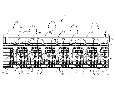
device base 125 of the detection device 104, through/into which the lights
guides 118 may each
extend. In some examples, each of the substrate layers may include
interconnected conductive
elements that forms at least part of the device circuitry 146, and dielectric
material 142 adjacent
to (and potentially surrounding) the conductive elements of the circuitry 146,
as shown in FIG. 3.
The conductive elements of the circuitry 146 may be embedded within the
dielectric material
142. As also shown in FIG. 3, the lights guides 118 may extend through the
dielectric material
142 and may be spaced from the circuitry 146. Various metallic elements and/or
dielectric
materials may be used, such as those suitable for integrated circuit
manufacturing (CMOS
manufacturing). For example, in some examples, the conductive
elements/circuity 146 may be
metallic elements, such as W (tungsten) elements, Cu (copper) elements, Al
(aluminum)
elements, or a combination thereof (but it is understood that other materials
and configurations
may be used). In some examples, the dielectric material may be SiO2 (but it is
understood that
other materials and configurations may be used).
[0062] As used herein, the term "layer" is not limited to a single continuous
body of material
unless otherwise noted. For example, the sensor layer 141 and/or the device
layers of the device
base 125 may include multiple sub-layers that are different materials and/or
may include
coatings, adhesives, and the like. Furthermore, one or more of the layers (or
sub-layers) may be
modified (e.g., etched, deposited with material, etc.) to provide the features
described herein.
[0063] As shown in FIGS. 3 and 4, the reaction structure 126 may comprise of
one or more
layers that form the reaction recesses 104 extending therein. The reaction
structure 126 may
extend along a top outer surface of the device base 125. In the illustrated
example, the reaction
18
CA 03067424 2019-11-29
WO 2019/125690 PCT/US2018/062019
structure 126 is deposited directly along the top or outer surface of a first
liner layer 154 and the
first and second filter material 116, 115 of the device base 125, as described
further below.
However, an intervening layer may be disposed between the reaction structure
126 and the
device base 125 in other examples. The reaction structure 126 may include one
or more
materials that are configured to allow the excitation light signals 101 and
emitted light signals
from the reaction sites 114 (after treatment with the reaction solution)
within the recesses 108 to
pass therethrough and into an opening 158 of one or more light guide 118
corresponding to a
particular reaction recess 108. In some examples, the reaction structure 126
may include one
more layer or other feature that prevents crosstalk or "sharing" of emitted
light from a particular
reaction site 114/reaction recesses 108 from to a non-corresponding sensor
140.
[0064] The reaction structure 126 may comprise a plurality of differing
layers, as shown in
FIGS. 3 and 4. In the illustrated example, the reaction structure 126 may
include a first reaction
layer 160 that extends over (directly or indirectly) device base 125 (e.g.,
over the first liner layer
154) and the opening 158 of the light guides 118 (e.g., the first and second
filter material 116,
115) of the device base 125, as shown in FIGS. 3 and 4. As also shown in FIGS.
3 and 4, in the
illustrated example, the reaction structure 126 further includes a second
layer 162 that extends
over (directly or indirectly) the first layer 160. The reaction structure 126
of illustrated example
also includes a third layer 164 that extends over (directly or indirectly) the
second layer 162, and
a fourth layer 166 that extends over (directly or indirectly) the third layer
162. The reaction
recesses 108 may extend at least into the third layer 164.
[0065] The fourth layer 166 may form the inner surfaces (e.g., side walls and
a bottom wall) of
the reaction recesses 108 by extending over an indentation (e.g., a cavity or
a void) in the third
layer 162, as shown in FIGS. 3 and 4. The fourth layer 166, and potentially
the second layer
162, may form the detector surface 112, as shown in FIGS. 3 and 4. In some
cases, the fourth
layer 166, and potentially the second layer 162, may be configured to provide
a solid surface that
permits chemicals, biomolecules or other analytes-of-interest to be
immobilized thereon. For
example, each of the reaction sites 114 may include a cluster of biomolecules
that are
immobilized to the detector surface 112, which may comprise the fourth layer
166, and
potentially the second layer 162. Thus, the fourth layer 166, and potentially
the second layer
162, may comprise a material that peintits the reaction sites 114 to be
immobilized thereto. The
first layer 160 and the fourth layer 166 (and potentially the second layer 162
and the third layer
19
CA 03067424 2019-11-29
WO 2019/125690 PCT/US2018/062019
166) may comprise a material that is at least substantially transparent to the
excitation light 101
and the emission light of the reaction sites 114. In addition, the fourth
layer 166, and potentially
the second layer 162, may be physically or chemically modified to facilitate
immobilizing the
biomolecules and/or to facilitate detection of the light emissions.
[0066] By way of example and as shown in the illustrated example of FIGS. 3
and 4, the first
layer 160 and the third layer 166 may comprise a first material, and the
second layer 162 and the
fourth layer 168 may comprise a second material that differs from the first
material. In some
such examples, the first material is SiN, and the second material is Ta0.
However, the reaction
structure 126 may comprise differing layers (e.g., different layers, fewer
layers, and/or additional
layers) and/or differing materials.
[0067] As shown in FIGS. 3 and 4, the device base 125 of the detection device
104 may include
a first shield layer 150 that extends over (directly or indirectly) the
stacked layers (e.g., metal-
dielectric layers) of the device base 125, such as over the dielectric
material 142 and the
conductive circuity components 146. The first shield layer 150 may include a
material that is
configured to block, reflect, and/or significantly attenuate the excitation
light 101 and/or the light
emissions from the reaction sites 114 (e.g., light signals that are
propagating from the flow
channel 118). By way of example only, the first shield layer 150 may comprise
tungsten (W).
[0068] The first shield layer 150 may include at least one an aperture
therethrough which
aligns, at least partially, with at least one corresponding light guide 118.
The first shield layer
150 may include an array of such apertures. In some examples, the first shield
layer 150 may
extend entirely about the apertures therein. As such, the light signals from
excitation
light 101 and/or the light emissions from the reaction sites 114 may be
blocked, reflected, and/or
significantly attenuated to prevent the light signals from passing through the
device base 125
outside of the light guides 118 and being detected by the light sensors 140.
In some examples,
the first shield layer 150 extends continuously between adjacent apertures or
light guides 118
and/or openings extending thereto. In some other examples, the first shield
layer 150 does not
extend continuously between adjacent apertures or light guides 118 such that
one or more other
aperture exists in the first shield layer 150, which may allow the excitation
light 101 and/or the
light emissions from the reaction sites 114 to pass therethrough.
[0069] In some examples, the device base 125 of the detection device 104 may
include a second
shield layer 152 that extends over (directly or indirectly) the first shield
layer 150, as shown in
CA 03067424 2019-11-29
WO 2019/125690 PCT/US2018/062019
FIGS. 3 and 4. The second shield layer 152 may include anti-reflective
material and/or a
material that prevents contamination of the underlying portions of the device
base 125. By way
of example only, the second shield layer 152 may comprise SiON. In some
examples, the
second shield layer 152 may be configured to prevent contaminated, such as
sodium, from
interacting with the first shield layer 150, the dielectric material 142
and/or the conductive (e.g.,
metal) components of the device circuitry 146. In some examples, the second
shield
layer 152 may mimic the configuration of the first shield layer 150. For
example, the second
shield layer 152 may include at least one aperture therethrough which aligns,
at least partially,
with at least one light guide 118, as shown in FIGS. 3 and 4. The second
shield layer 152 may
include an array of such apertures. In some examples, the second shield layer
152 may extend
about the apertures therein. In some examples, the second shield layer 152
extends continuously
between adjacent light guides 118 and/or openings extending thereto. In some
other examples,
the second shield layer 152 does not extend continuously between adjacent
light guides 118
and/or openings extending thereto such that one or more other aperture exists
in the second
shield layer 152, as shown in FIGS. 3 and 4.
[0070] In some examples, the light detection device 104 may include a first
liner layer 154 that
extends over the device base 125 and about the light guides 118, as shown in
FIGS. 3 and 4. The
first liner layer 154 may be a continuous conformal layer formed on the device
base 125. The
first liner layer 154 may be void of defined apertures. However, the first
liner layer 154 may
include internal discontinuities, pores, breaks or the like that allow a
liquid or solution, such as
the reaction solution, to flow therethrough, as explained further below. The
first liner layer 154
may be chemically reactive with respect to the reaction solution. For example,
due to the
composition (e.g., water and/or oil) and/or relatively high acidity (e.g., a
pH equal to or less than
about 5) or relatively high basicity (e.g., a pH equal to or greater than
about 8) of the reaction
solution, the reaction solution may chemically react with the material of the
first liner layer 154
when exposed thereto and cause the material to be dissolved or otherwise
detached (i.e., etch the
liner layer 154). Over an exposure time, the reaction solution may thereby
etch through the first
liner layer 154 and, ultimately, interact with and corrode or otherwise
interfere with the
functioning of the device circuitry 146. For example, the first liner layer
154 may be a silicon
nitride layer (or otherwise include SiN), and the relatively high acidic or
basic reaction solution
may etch the SiN when exposed thereto.
21
CA 03067424 2019-11-29
WO 2019/125690 PCT/US2018/062019
[0071] In the illustrated examples, the first liner layer 154 extends between
the reaction
structure 126 and the second shield layer 152 on the top upper portion of the
device base 125
(and/or any layer on the top or upper portion of the device base 125) in the
interstitial regions
113, and extends along the light guides 118, as shown in FIGS. 3 and 4. In the
illustrated
example, the first liner layer 154 extends about the light guides 118 and
adjacent the dielectric
material 142 of the device base 125, as shown in FIGS. 3 and 4. As also shown
in FIGS. 3 and
4, the first liner layer 154 may extend about the light guides 118 such that
it is positioned
between (e.g., directly between) the dielectric material 142 of the device
base 125 and the
support liner 130 and second filter region 115 of the light guides 118. The
first liner layer
154 may be configured as an anti-reflective layer or a reflective layer (e.g.,
to ensure the light
emitted from the reaction sites 114 passes through the light guides 118), a
contamination
prevention layer (e.g., to prevent sodium contamination into the device base
125) and/or an
adhesion layer (e.g., to adhere the support liner 130 and second filter region
115 of the light
guides 118 to the dielectric material 142). In some examples, the liner layer
154 may be
configured as a contamination prevention layer that prevents any ionic species
from penetrating
into device layers (e.g., metal-dielectric layers). In some examples, the
liner layer 154 comprises
SiN. In some examples, the liner layer 154 comprises a SiN layer.
[0072] As shown in FIGS. 3 and 4, the first liner layer 154 may be of a
substantially uniform
thickness. In other examples, the thickness of the first liner layer 154 may
vary. For example,
the portions of the first liner layer 154 extending over the top portion of
the device base 125 may
be a first thickness, and the portions of the of the first liner layer 154
extending about the light
guides 118 may be a second thickness that is thicker or thinner than the first
thickness. As
another example, the thickness of the portions of the of the first liner layer
154 extending about
the light guides 118 may be vary along the depth of the within the device base
125 (e.g., may
taper with depth into the device base 125). In some examples, the thickness of
the first liner
layer 154 may be within the range of about 10 nm to about 100 nm. In the
illustrated example,
the first liner layer 154 is about 50 nm thick.
[0073] As shown in FIG. 3, the device base 125 may also include a second liner
layer 155
positioned within the device layers and beneath the light guides 118. The
second liner layer 155
may be substantially similar or the same as the first liner layer 154 but for
its position within the
device base 125. In some examples, the second liner layer 155 may extend
immediately below
22
CA 03067424 2019-11-29
WO 2019/125690 PCT/US2018/062019
the support liner 130 along the bottom of the light guides 118, as shown in
FIG. 3. In this way,
the first liner layer 154 and the second liner layer 155 may extend entirely
about the light guides
118 but for the openings 158 of the light guides 118 beneath the reaction
recesses 108.
[0074] As discussed above, the device base 125 of the detection device 104 may
include the
support liner or layer 130 positioned at a bottom portion of the light guides
118, as shown in
FIG. 3. The support liner 130 may extend (directly or indirectly) between the
first filter region
116 and the dielectric material 142, and between the first filter region 116
and the second liner
layer 155. For example, the support liner 130 may extend about the first
filter region 116 and
between (directly or indirectly) the first filter region 116 and the first
liner layer 154, as shown in
FIG. 3. In this way, the support liner 130 may extend about a bottom portion
of the first filter
region 116, including about the side and bottom surfaces thereof The support
liner 130 may
extend fully about the first filter material 116 of the light guides 118. As
shown in FIG 3, the
second filter region 115 may extend above the support liner 130 in an upper
portion of the light
guides 118. The support liner 130 may thereby support or extend below the
second filter region
115. In some examples, the support liner 130 may extend immediately below the
second filter
region 115. The support liner 130 and the second filter region 115 may thereby
combine to form
a layer that extends about the first filter material 116 and is positioned
between the first filter
material 116 and the first liner layer 154 and/or dielectric material 142 of
the device base 125, as
shown in FIG. 3.
[0075] The thickness of the support liner 130 may be any thickness. In some
examples, the
thickness of the support liner 130 may be within the range of about 100 nm and
about 1 micron,
or within the range of about 100 nm and about 500 nm. In some examples, the
thickness of the
support liner 130 may be the same or substantially similar thickness to the
thickness of the
second filter region 115, such as at least the portion of the support liner
130 that abuts or is
positioned proximate to the second filter region 115. In some examples, the
thickness of the
support liner 130 below the first filter region 116 at the bottom of the light
guides 118 (between
the first filter region 116 and the second liner layer 155 and/or dielectric
material 142) may be
the same or substantially similar thickness as the thickness of the support
liner 130 extending
about the side surfaces of the first filter region 116 (between the first
filter region 116 and the
first liner layer 154 and/or dielectric material 142).
23
CA 03067424 2019-11-29
WO 2019/125690 PCT/US2018/062019
[0076] The support liner 130 may be void of predefined apertures or other
voids that would
allow a liquid or solution, such as the reaction solution, to flow
therethrough. The support liner
130 may also be void of any internal discontinuities, pores, cracks, breaks or
the like, or prevent
the formation thereof, that would allow a liquid or solution, such as the
reaction solution, to flow
therethrough. The support liner 130 may thereby be a liquid impervious barrier
layer. A liquid
impervious layer herein refers to a layer that may prevent any liquid or
solution (e.g., the
reaction solution) from passing therethrough, such as preventing at least
about 99 vol% of the
reaction solution in contact with the protection layer 130 at atmospheric
pressure from passing
therethrough. The support liner 130 may also be chemically inert with respect
to the reaction
solution such that the reaction solution (which may include a relatively high
acidity or relatively
high basicity, as described above) does not etch the support liner 130, or
etches less than about
one (1) angstrom (A) of the thickness of the support liner 130 per hour at
about 100 degrees
Celsius and at about atmospheric pressure, when the reaction solution is in
contact with the
support liner 130. For example, the composition of the support liner 130 may
not chemically
react, or chemically reacts to only a relatively small degree, with the
composition of the reaction
solution (which may include a relatively high acidity or relatively high
basicity) such that the
reaction solution does not etch the support liner 130 or etches less than
about one (1) angstrom
(A) of the thickness of the support liner 130 per hour at about 100 degrees
Celsius and at about
atmospheric pressure when the reaction solution is in contact with the support
liner 130. The
support liner 130 may thereby comprise an etch resistant layer with respect to
the reaction
solution (which may include a pH equal to or less than about 5 or a pH equal
to or greater than
about 8, for example) to prevent the reaction solution from penetrating
therethrough (over time)
and, ultimately, interacting with and corroding or otherwise interfering with
the functioning of
the device circuitry 146. The support liner 130 is thereby configured to
prevent a liquid or
solution (such as the reaction solution) that may penetrate through the
reaction structure 126 and
the filter material 116 of a light guide 118 to the support liner 130 from
interacting with the
device circuitry 146.
[0077] The support liner 130 may comprise any material that differs from the
material of the
first liner layer 154 and the first filter material 116, and such that it
allows light emitted from the
reaction sites 114 to pass therethrough and to the at least one corresponding
light sensor 140 via
the corresponding light guide 118. For example, the support liner 130 may
comprise any
24
CA 03067424 2019-11-29
WO 2019/125690 PCT/US2018/062019
material that allows light emitted from the reaction sites 114 of an
associated reaction recess 108
that is not filtered by the first and second filter regions 116, 115 to pass
therethrough. As
explained further below, the support liner 130 may comprise any material that
differs from the
material of the first liner layer 154 and the first filter material 116 so
that an upper portion of the
support liner 130 can be selectively removed (e.g., etched) to form the
support liner 130 only in
the lower or bottom portion of the light guides 118. In some examples, the
support liner 130
may comprise an oxide, a nitride, or a combination thereof. In some such
examples, the support
liner 130 may comprise of SiO2, a metal oxide or a combination thereof.
[0078] In some examples, the support liner 130 may comprise material that is
chemically inert
to the reaction solution. For example, the support liner 130 may comprise any
material that does
not chemically react, or chemically reacts to only a relatively small degree,
with the reaction
solution (which may include a pH equal to or less than about 5 or a pH equal
to or greater than
about 8, for example) such that the reaction solution does not etch the
support liner 130 or etches
less than about one (1) angstrom (A) of the thickness of the support liner 130
per hour at about
100 degrees Celsius and at about atmospheric pressure when the reaction
solution is in contact
with the support liner 130. For example, the support liner 130 may comprise an
oxide, a nitride,
or a combination thereof. In some examples, the support liner 130 may comprise
silicon dioxide,
a metal oxide, a metal nitride or a combination thereof. In some examples, the
support liner 130
may comprise silicon dioxide, silicon oxynitride, silicon monoxide, silicon
carbide, silicon
oxycarbide, silicon nitrocarbide, silicon dioxide, metal oxide, metal nitride
or a combination
thereof. In some examples, the pH of the reaction solution is greater than or
equal to about 8,
and the support liner 130 may comprise silicon dioxide, silicon oxynitride,
silicon monoxide,
silicon carbide, silicon oxycarbide, silicon nitrocarbide, silicon dioxide,
metal oxide, metal
nitride or a combination thereof. In some examples, the pH of the reaction
solution is less than
or equal to about 5, and the support liner 130 comprises silicon carbide,
silicon oxycarbide,
silicon nitrocarbide, a metal oxide, a metal nitride or a combination thereof.
[0079] As discussed above, the light guides 118 may extend from an opening 158
into the
device base 125, such as through the dielectric material layers 142 and toward
at least one image
sensor 140. In particular examples, the light guides 118 are elongated and
extend from
proximate to at least one corresponding reaction recess 108 from the aperture
158 thereof toward
at least one corresponding light sensor 140 within the sensor layer 141. The
light guides 118
CA 03067424 2019-11-29
WO 2019/125690 PCT/US2018/062019
may extend lengthwise along a central longitudinal axis. The light guides 118
may be
configured in a three-dimensional shape that allows and/or promotes the light
emitted from the
reaction site(s) 112 of at least one corresponding reaction recess 108 to the
at least one
corresponding light sensor 140, such as substantially cylindrical or frusto-
conical shape with a
circular opening 158. The longitudinal axis of the light guides 118 may extend
through a
geometric center of the cross-section. However, other geometries may be used
in alternative
examples. For example, the cross-section of the light guides 118 may be
substantially square-
shaped or octagonal. The light guides 118 may comprise the first filter region
116, the second
filter region 115 and the support liner 130.
[0080] As discussed above and shown in FIGS. 3 and 4, light guides 118 may
include the first
filter region 116 and the second filter region 115. The first filter region
116 may be frusto-
conical, and the second filter region 115 may be an annual sleeve or liner
that extends about the
first filter region 116 (above the annual support liner or sleeve 130). The
first filter region 116
may comprise a first filter material that is configured to filter the
excitation light 101 of a first
wavelength or a range of wavelengths (and potentially a fourth wavelength or a
range of
wavelengths), and permit the light emissions of a second wavelength or a range
of
wavelengths from at least one reaction site 114 of at least one corresponding
reaction recess 108
to propagate therethrough and toward at least one corresponding light sensor
140. Similarly, the
second filter region 115 may comprise a second filter material that is
configured to filter the
excitation light 101 of the first wavelength or a range of wavelengths (and
potentially the fourth
wavelength or a range of wavelengths), and permit the light emissions of a
third wavelength or a
range of wavelengths from at least one reaction site 114 of the at least one
corresponding
reaction recess 108 to propagate therethrough and toward the at least one
corresponding light
sensor 140. In some examples, the first filter region 116 may also filter the
light emissions of the
third wavelength or a range of wavelengths from the at least one reaction site
114 (i.e., prevent
such emitted light from passing therethrough), and/or the second filter region
115 may also filter
the light emissions of the second wavelength or a range of wavelengths from
the at least one
reaction site 114 (i.e., prevent such emitted light from passing
therethrough). In other examples,
the first filter region 116 may allow the light emissions of the third
wavelength or a range of
wavelengths from the at least one reaction site 114 to pass therethrough,
and/or the second filter
region 115 may allow the light emissions of the second wavelength or a range
of
26
CA 03067424 2019-11-29
WO 2019/125690 PCT/US2018/062019
wavelengths from the at least one reaction site 114 to pass therethrough. Each
of the light guides
118 of the array light guides 118 of the device 104 may include substantially
the same
configuration (e.g., filtering properties) of the first and second filter
regions 116, 115, or
differing light guides 118 may include differing configurations (e.g.,
filtering properties) of the
first and second filter regions 116, 115.
[0081] The first filter region 116 and the second filter region 115 of the
light guide 118 may be,
for example, absorption filters (e.g., an organic absorption filter) such that
they absorb a
respective wavelengths or ranges of wavelengths and allow at least one
predetermined
wavelength or range of wavelengths to pass therethrough. By way of an example
only, at least
one first reaction site 114 of at least one reaction recess 108 of the device
104 may be configured
to produce first light emissions of a first wavelength or range of wavelengths
upon incident
excitation light 101 of a third wavelength or range of wavelengths, and at
least one second
reaction site 114 of at least one reaction recess 108 of the device 104 may be
configured to
produce second light emissions of a second wavelength or range of wavelengths
upon incident
excitation light 101 of the third wavelength or range of wavelengths that
differs (or does not
overlap) from the first light emissions. The first and second reaction sites
114 may be the same
reaction site 114, may be differing reaction sites 114 provided within a
common reaction recess
108, or may be may be differing reaction sites 114 provided within differing
reaction recesses
108. In such an example, the first filter region 116 may absorb the excitation
light 101 and the
second light emissions, but allow the first light emissions from the first
reaction sites to pass
therethrough. Similarly, the second filter region 115 may absorb the
excitation light 101 and the
first light emissions, but allow the second light emissions from the first
reaction sites to pass
therethrough.
[0082] By way of another example, at least one first reaction site 114 of at
least one reaction
recess 108 of the device 104 may be configured to produce first light
emissions of a first
wavelength or range of wavelengths upon incident first excitation light 101 of
a third wavelength
or range of wavelengths, and at least one second reaction site 114 of at least
one reaction recess
108 of the device 104 may be configured to produce second light emissions of a
second
wavelength or range of wavelengths upon incident second excitation light 101
of a fourth
wavelength or range of wavelengths. The first, second, third and fourth
wavelengths or ranges of
wavelengths may differ (and not overlap, if ranges of wavelengths). The third
and fourth
27
CA 03067424 2019-11-29
WO 2019/125690 PCT/US2018/062019
excitation light 101 may be emitted at the same time (e.g., during the same
light detection event),
or the third and fourth excitation light 101 may be independently or
separately emitted at
differing times (e.g., during differing light detection events). The first and
second reaction sites
114 may be the same reaction site 114, may be differing reaction sites 114
provided within a
common reaction recess 108, or may be may be differing reaction sites 114
provided within
differing reaction recesses 108. In such an example, the first filter region
116 may absorb at
least the first excitation light 101 and the second light emissions, but allow
the first light
emissions from the first reaction sites to pass therethrough. The first filter
region 116 may also
absorb the second excitation light 101. Similarly, the second filter region
115 may absorb at
least the second excitation light 101 and the first light emissions, but allow
the second light
emissions from the first reaction sites to pass therethrough. The second
filter region 115 may
also absorb the first excitation light 101.
[0083] The material of the first and second filter regions 116, 115 may be any
material that
prevents the excitation light from passing therethrough (e.g., reflects,
refracts and/or absorbs
such light) and allows emitted light (from at least one reaction site 114) of
a predefined or
predetermined wavelength or range of wavelengths therethrough. For example,
the material of
the first and second filter regions 116, 115 may be a polymer material (the
same polymer
material or a different polymer material) with different dyes. For example,
the material of the
first and second filter regions 116, 115 may be a polymer material (the same
polymer material or
a different polymer material) with different dyes. In such examples, the
polymer material may
include a C-H-0 based matrix, and the differing dyes may be differing metal
organic complex
molecules, for example. However, any other appropriate material may be used.
As discussed
above, in some examples the first and second filter regions 116, 115 may allow
emitted light
(from at least one reaction site 114) of differing wavelengths or ranges of
wavelengths from
passing therethrough. As such, in some examples the first filter region 116 of
a light guide 118
may filter (i.e., block) emitted light (from at least one reaction site 114)
that the second filter
region 115 of the light guide 118 allows to pass therethrough, and/or the
second filter region 115
of a light guide 118 may filter (i.e., block) emitted light (from at least one
reaction site 114) that
the first filter region 116 of the light guide 118 allows to pass
therethrough.
[0084] Each light guide 118 may thereby be configured relative to surrounding
material of the
device base 125 (e.g., the dielectric material 142 and/or the first and second
liner layers 154,
28
CA 03067424 2019-11-29
WO 2019/125690 PCT/US2018/062019
155) to form a light-guiding structure. For example, the light guides 118 may
have a refractive
index of at least about 2. In certain examples, the light guide 118 is
configured such that the
optical density (OD) or absorbance of the excitation light is at least about 4
OD. More
specifically, the filter material 116 of the light guides 118 may be selected
and the light guide
118 may be dimensioned to achieve at least about 4 OD. In more particular
examples, the light
guide 118 may be configured to achieve at least about 5 OD, or at least about
6 OD.
[0085] Initially, the reaction sites 114 of one or more reaction recesses 114
of the reaction
structure 126 of the device 104 or bio assembly 100 may not include a
designated reaction. As
discussed above, a reaction site 114 may include biological or chemical
substances immobilized
to the detector surface 112 or, more specifically, on the base and/or side
surfaces of the reaction
recesses 108. In particular examples, the reaction sites 114 are located
proximate to an opening
158 of at least one corresponding light guide 118 so that pre-designated light
emissions emitted
from the reaction sites 114 after a designated reaction has taken place (via
treatment with the
reaction solution) propagate through the reaction structure 126, through the
opening 158 and the
first and/or second filter material 116, 115, through the support liner 130
(and potentially the first
and/or second liner layers 154, 155), and to at least one corresponding light
sensor 140.
[0086] The biological or chemical substances of a single reaction site 114 may
be similar or
identical (e.g., a colony of analytes (e.g., oligonucleotides) that have a
common sequence).
However, in other examples, a single reaction site 114 and/or reaction recess
may include
differing biological or chemical substances. Similarly, reaction sites 114 of
a single reaction
recess 108 may include different biological or chemical substances (and
thereby designated
reactions, with differing fluorescent labels). Before a designated reaction,
the reaction
sites 114 may include at least one analyte (e.g., an analyte-of-interest). For
example, the analyte
may be an oligonucleotide or a colony thereof (e.g., an oligonucleotide-of-
interest). The
oligonucleotides may have an effectively common sequence and bind with a
predefined or
particular fluorescently labeled biomolecule, such as a fluorescently-labeled
nucleotide.
Different reaction sites 114 may thereby include differing fluorescently
labeled biomolecules,
such as differently fluorescently-labeled nucleotides.
[0087] However, prior to the designated reaction, the fluorophores of the
fluorescently labeled
biomolecule are not incorporated or bonded to the biological or chemical
substances (e.g., an
oligonucleotides) at the reaction sites 114. To achieve or obtain a designated
reaction (i.e., to
29
CA 03067424 2019-11-29
WO 2019/125690 PCT/US2018/062019
incorporate the fluorescently labeled biomolecule with the biological or
chemical
substances at/of the reaction sites 114), a flow cell may provide a flow of
reaction solution 170 to
the reaction structure 126 of the light detection device 104, as shown in FIG.
5. In this way, the
reaction solution 170 may initiate a reaction and/or form a reaction product
at the reaction
sites 114 that generates light emissions upon incident excitation light.
[0088] The reaction solution may comprise one or more sequencing reagents
utilized for DNA
grafting, clustering, cleaving, incorporating and/or reading, for example.
However, the reaction
solution may be any solution. For example, the reaction solution 170 may be an
aqueous
solution and/or may be comprised of an oil; however, it is understood that the
reaction solution
170 may comprise any other liquid. The reaction solution 170 may include one
or more
constituents that would tend to react with, corrode, dissolve, deteriorate or
otherwise render the
circuity 146 inoperable or less effective as circuitry (i.e., transferring
signals or electrons). For
example, the reaction solution 170 may be an aqueous solution that would tend
to oxidize the
metal portions of the circuity 146 if it interacted therewith.
[0089] In one example, the reaction solution 170 contains one or more
nucleotide types, at least
some of which are fluorescently-labeled, and the reaction solution 170 also
contains one or more
biomolecules, such as polymerase enzymes, which incorporate nucleotides into a
growing
oligonucleotide at the reaction site 114, thereby labeling the oligonucleotide
with a fluorescently-
labeled nucleotide. In this implementation, the flow cell provides a wash
solution to remove any
free nucleotides that did not get incorporated into oligonucleotides. The
reaction sites 114 are
then illuminated with an excitation light 101 of a first wavelength, causing
fluorescence of a
second or third wavelength in those reaction sites 114 where a fluorescently-
labeled nucleotide
was incorporated. Reaction sites 114 that did not incorporate a fluorescently-
labeled nucleotide
do not emit light.
[0090] As shown in the illustrated example in FIG 5, the reaction solution 170
may be
provided within the retraction recesses 118 to achieve the designated
reactions, such as at least
one fluorescently-labeled molecule binding or incorporating with the
biological or chemical
substances immobilized at the reaction sites 114. In some examples, the
biological or chemical
substances of the reaction sites 114 may be an analyte, and the fluorescently-
labeled molecule
may include at least one fluorophore that bonds or incorporates with the
analyte. In such
examples, the analyte may comprise an oligonucleotide, and the at least one
fluorescently-
CA 03067424 2019-11-29
WO 2019/125690 PCT/US2018/062019
labeled molecule comprises a fluorescently-labeled nucleotide. The reaction
solution 170 may
include differing fluorescently-labeled molecules that emit light of differing
wavelengths or
ranges of wavelengths in response to incident excitation light. Differing
reaction sites 114 (of
the same or differing reaction recesses 108) may thereby be configured to emit
light of differing
wavelengths or ranges of wavelengths in response to incident excitation light.
[0091] When the biological or chemical substances (e.g., oligonucleotides) of
the reaction
sites 114 are similar or identical, such as having a common sequence, the
reaction sites 114 may
be configured to generate common light emissions after the designated reaction
and the
excitation light 101 is absorbed by fluorescently-labeled molecules bonded or
incorporated
therewith from the reaction solution 170. When biological or chemical
substances (e.g.,
oligonucleotides) of the reaction sites 114 are different, such as having
different sequences, the
reaction sites 114 may be configured to generate different light emissions
(different wavelengths
or ranges or wavelengths) after the designated reactions and the excitation
light 101 is absorbed
by differing fluorescently-labeled molecules bonded or incorporated therewith
(e.g., provided by
the reaction solution 170). In this way, the first filter region 116 of the
light guides 118 may be
selected or configured to allow light emissions from reaction sites 114 with a
first designated
reaction to propagate therethrough and to the corresponding light sensor 140
(and prevent the
excitation light, and potentially light emissions from reaction sites 114 with
second designated
reactions, from passing therethrough to the corresponding light sensor 140),
and the second filter
region 115 of the light guides 118 may be selected or configured to allow
light emissions from
reaction sites 114 with a second designated reaction that differs from the
first designated reaction
(e.g., including different fluorescently-labeled molecules that emit light of
differing wavelengths
or ranges of wavelengths) to propagate therethrough and to the corresponding
light sensor 140
(and prevent the excitation light, and potentially light emissions from
reaction sites 114 with the
first designated reactions, from passing therethrough to the corresponding
light sensor 140).
[0092] As shown in FIG. 6, after the reaction solution 170 has interacted with
the biological or
chemical substances (e.g., oligonucleotides) of the reaction sites 114, the
designated reactions
have occurred such that the reaction sites 114 include fluorescently-labeled
molecules (the same
or different fluorescently-labeled molecules), such as fluorophores, that emit
light of a
predefined or predetermine wavelength or range of wavelengths when excited by
the excitation
light 101 (i.e., when the excitation light 101 is incident upon the reaction
sites 114). The
31
CA 03067424 2019-11-29
WO 2019/125690 PCT/US2018/062019
excitation light 101 may thereby be configured based on the fluorescently-
labeled molecules of
the reaction solution 170, or vice-versa. As shown in FIG. 6, when excited by
the excitation
light 101, the reaction sites 114 may emit emitted light 172 or signals of a
wavelength or range
of wavelengths that differs from excitation light 101.
[0093] As shown in FIG. 6, the emitted light 172 from the reaction sites 114
may emit in all
directions (e.g., isotropically) such that, for example, a portion of the
emitted light 172 is
directed into the at least one corresponding light guide 118, and a portion of
the light 172 is
directed into the flow channel 119 or the reaction structure 126. For the
portion that is directed
into the light guide 118, the devices 104 is configured to facilitate
detection of the photons by the
at least one corresponding light sensor 140. Specifically, the emitted light
172 from the reaction
sites 114 that passes through the opening 158 of a corresponding light guide
118 will propagate
through the first or second filter region 116, 115 thereof to the light sensor
140. The excitation
light 101, however, will be absorbed or otherwise prevented from propagating
through the light
guide 118 to the light sensor 140 by the first and/or second filter region
116, 115, as shown in
FIG. 6.
[0094] As shown in FIG. 6, some of the reaction sites 114 may be configured to
emit light 172
of a first wavelength or range of wavelengths that is not filtered by the
first filter region 116 but
is filtered (i.e., prevented from passing through) by the second filter region
115, and some of the
reaction sites 114 may be configured to emit light 172 of a second wavelength
or range of
wavelengths that is not filtered by the second filter region 115 but is
filtered (i.e., prevented from
passing through) by the first filter region 116. As noted above, in some
examples some reaction
sites 114 of the device 104 may be configured to emit light 172 of the first
wavelength or range
of wavelengths upon incident excitation light 101 of a third wavelength, and
some other reaction
sites 114 of the device 104 may be configured to emit light 172 of the second
wavelength or
range of wavelengths upon the incident excitation light 101 of the third
wavelength. In such an
example, the first and second filter regions 116, 115 may both be configured
to filter the
excitation light 101 of the third wavelength. Still further, in some other
examples some reaction
sites 114 of the device 104 may be configured to emit light 172 of the first
wavelength or range
of wavelengths upon incident excitation light 101 of a third wavelength or
range of wavelengths,
and some other reaction sites 114 of the device 104 may be configured to emit
light 172 of the
second wavelength or range of wavelengths upon the incident excitation light
101 of a fourth
32
CA 03067424 2019-11-29
WO 2019/125690 PCT/US2018/062019
wavelength or range of wavelengths. In such an example, the first and second
filter regions 116,
115 may both be configured to filter the excitation light 101 of the third and
fourth wavelength
or ranges of wavelengths, or the first and second filter regions 116, 115 may
be configured to
filter one of the excitation light 101 of the third and fourth wavelengths or
ranges of wavelengths
(e.g., the first filter region 116 may be configured to filter the excitation
light 101 of the third
wavelength or range of wavelengths, and the second filter region 115 may be
configured to filter
the excitation light 101 of the fourth wavelength or range of wavelengths).
The device circuitry
146 that is electrically coupled to the light sensors 140 transmits data
signals based on the
photons detected by the light sensors 140. In this way, only the presence of a
designated reaction
at a reaction site 114 via treatment with the reaction solution will cause
emitted light 172 to be
detected by the light sensors 140 during a light detection even (i.e., a
reaction that results in
emittance light 172 that is not filtered by at least one of the first and
second filter regions 116,
115).
[0095] As shown in FIG. 6, a portion of the emitted light 172 from the
reaction sites(s) 114 that
passes into the at least one corresponding light guide 118 may propagate
directly through the
first filter material 116 or the second filter material 115 thereof and to the
at least one
corresponding light sensor 140. For example, at least a majority of the
emissive light 172 from
the reaction sites(s) 114 that passes into the at least one corresponding
light guide 118 via the
opening 158 may pass directly (e.g., linearly or substantially linearly)
through the first filter
material 116 or the second filter material 115 to the at least one
corresponding light sensor 140.
A small amount of the emissive light 172 from the reaction sites(s) 114 that
passes into the at
least one corresponding light guide 118 may travel at an angle such that it
passes through the
support liner 130, the liner layer 154 and into the dielectric material layers
142. Such light may
be reflected by the circuitry 146 or other metal or reflective structures
embedded within the
dielectric material layers 142, and potentially back into the corresponding
light guide 118 (and
potentially to the at least one corresponding light sensor 140). In some
examples, the support
liner 130 and/or the liner layer 154 may be transparent to light, such as
transparent or
substantially transparent at least to the emissive light 172 from the reaction
sites(s) 114.
[0096] FIGS. 7-13 illustrates an example of a method 200 of manufacturing a
light detection
device, such as the light detection device 104 of FIGS. 1-6. Therefore, like
reference numerals
preceded with "2," as opposed to "1," are used to indicate like components,
aspects, functions,
33
CA 03067424 2019-11-29
WO 2019/125690 PCT/US2018/062019
processes or functions, and the description above directed thereto equally
applies, and is not
repeated for brevity and clarity purposes. The method 200, for example, may
employ structures
or aspects of various examples (e.g., systems and/or methods) discussed
herein. In various
examples, certain steps may be omitted or added, certain steps may be
combined, certain steps
may be performed simultaneously, certain steps may be performed concurrently,
certain steps
may be split into multiple steps, certain steps may be performed in a
different order, or certain
steps or series of steps may be re-performed in an iterative fashion.
[0097] As shown in FIGS. 7 and 8, the method 200 of forming a device 204 may
include
forming (at 270 of FIG. 7) a plurality or array of trenches or cavities 280
within a device base
225. As discussed above, the device base 225 may include an array of light
sensors 240 and
device circuitry 246 electrically coupled to the light sensors 240 that
transmit data signals based
on photons detected by the light sensors 240. The device base 225 may be
provided or obtained
via any process. For example, the device base 225 may be obtained in a
preassembled or
premanufactured state, or the device base 225 may be formed or manufactured
prior to forming
270 the plurality of trenches 280. The plurality of trenches may extend from
an outer, external
or top surface of the device base 225 and toward at least one corresponding
light sensor 240
(through the thickness of the device base 225).
[0098] As discussed above, the device base 225 may be manufactured using
integrated circuit
manufacturing technologies, such as CMOS manufacturing technologies. For
example, the
device base 225 may include several substrate layers (e.g., dielectric
material layers 242) with
different modified features (e.g., metallic elements) embedded therein that
form the device
circuitry 246. The plurality of trenches 280 may be formed in the substrate
layers (e.g., in the
dielectric material layers 242) to correspond to portions of the device base
225 that will include,
after the method 200, the light guides 218. While only one trench 280 is
depicted in FIG. 8, as
described above the device base 225 may include an array of light guides 218,
and therefore an
array of trenches 280 may be formed.
[0099] As shown in FIG. 8, the trenches 280 may extend through openings in the
first shield
layer 250 and/or second shield layer 252 and through the dielectric material
242 toward at least
one corresponding light sensor 240. As shown in FIG. 8, interior surfaces of
the device base
225, such as the dielectric material 242 thereof, may define the trenches 280
for the formation of
the light guides 218 therein. The trenches or cavities 280 may extend to the
second liner layer
34
CA 03067424 2019-11-29
WO 2019/125690 PCT/US2018/062019
255 that extends through the dielectric material 242. In this way, the second
liner layer 255 may
form the bottom of the trenches 280. As also shown in FIG. 8, other openings
in the first shield
layer 250 and/or second shield layer 252 may be formed in the interstitial
areas 213 of the device
base 225.
[0100] The trenches 280 may be formed by any process(es) or technique(s) that
removes the
portions of the dielectric material 242 (and potentially portions of the first
shield layer 250
and/or second shield layer 252). For example, the trenches 280 may be formed
by one or more
selective etching processes and/or reactive ion etching process. In one
example, the trenches 280
may be formed by applying at least one mask (not shown) to the device base 225
and removing
material (e.g., through etching) of the portions of the dielectric material
242 (and potentially
portions of the first shield layer 250 and/or second shield layer 252).
[0101] As shown in FIGS. 7 and 9, after formation of the plurality of trenches
280, the method
200 may include depositing (at 272 of FIG. 7) the first liner layer 254 over
the top surface of the
device base 225 and within the plurality of trenches 280. In some examples,
the first liner layer
254 may be formed over the sidewalls of the plurality of trenches 280 and not
over the second
liner layer 255 at the bottom of the trenches 280. In some other examples, the
first liner layer
254 may be formed over the second liner layer 255 at the bottom of the
trenches 280, but then
subsequently removed. The first liner layer 254 may be deposited over the
second shield layer
252 on the top surface of the device base 225, and potentially over any
openings in the openings
in the first shield layer 250 and/or second shield layer 252 in interstitial
areas 213 of the device
base 225 such that the second shield layer 252 extends over the dielectric
material 242 in such
openings, as shown in FIG. 9.
[0102] The first liner layer 254 may be configured as an anti-reflective layer
or a reflective
layer (e.g., to ensure the light emitted from reaction sites passes through
the light guides), a
contamination prevention layer (e.g., to prevent sodium contamination of the
circuitry) an
adhesion layer (e.g., to adhere filter material of the light guides to the
dielectric material) and/or.
In some examples, the first liner layer 254 may be configured as a
contamination prevention
layer that prevents any ionic species from penetrating into device layers
(e.g., metal-dielectric
layers). In some examples, the first liner layer 254 may comprise SiN.
[0103] The first liner layer 254 may be a continuous conformal layer formed on
the device base
225. The first liner layer 254 may be void of defined apertures. However, the
first liner layer
CA 03067424 2019-11-29
WO 2019/125690 PCT/US2018/062019
254 may include at least one internal discontinuity, pore, crack, break or the
like that allows a
liquid or solution, such as the reaction solution, to flow through the first
liner layer 254. For
example, the density of the first liner layer 254 may be relatively low such
that internal
discontinuities thereof form a pathway through the first liner layer 254. As
another example,
discontinuities extending through the first liner layer 254 may be formed by
the reaction solution
or any other liquid or solution) from reacting with and etching through the
first liner layer 254.
The discontinuities of the first liner layer 254 may allow a liquid or
solution (e.g., the reaction
solution) from passing therethrough and, ultimately, to the conductive (e.g.,
metal) components
of the device circuitry 246. As discussed above, the liquid or solution (e.g.,
the reaction solution
may corrode or otherwise interfere with the operation of the device circuitry
246.
[0104] The first liner layer 254 may be formed by any process(es) or
technique(s). For
example, the first liner layer 254 may be formed by at least one chemical
deposition process
(e.g., plating, chemical vapor deposition (CVD), plasma enhanced CVD (PECVD),
or atomic
layer deposition (ALD), for example), a physical deposition process, a growth
mode, epitaxy, or
a combination thereof. In some examples, the first liner layer 254 may be
formed conformally
over the surface of the device base 225 and within the trenches 280 (e.g.,
over the side walls and,
potentially, the bottom surface of the trenches 280). The first liner layer
254 may comprise a
substantially constant thickness, or the thickness may vary.
[0105] After formation of the first liner layer 254 on the device base 225
(and within the
trenches 280), the first liner layer 254 may be further processed. For
example, at least the
portion of the first liner layer 254 extending over the top surface of the
device base 225 (i.e., the
interstitial areas 213 of the first liner layer 254) may be processed to
planarize, flatten, smooth or
otherwise improve the surface topography thereof. In some such examples, at
least the portion
of the first liner layer 254 extending over the top surface of the device base
225 (i.e., the
interstitial areas 213 of the first liner layer 254) may be etched and/or
polished (e.g., chemical
and/or mechanical polishing/planarization) to planarize the outer surface of
the first liner layer
254.
[0106] As shown in FIGS. 7 and 10, the method 200 may include depositing (at
274 of FIG. 7)
the support liner 230 over the device base 225 such that it extends over the
top surface of the
device base 225 and within the plurality of trenches 280. In some examples,
the support liner
230 may be formed over the sidewalls of the plurality of trenches 280 and the
bottom of the
36
CA 03067424 2019-11-29
WO 2019/125690 PCT/US2018/062019
trenches 280. The support liner 230 may be formed over the first liner layer
254 and the second
liner layer 255.
[0107] The support liner 230 may be formed by any process(es) or technique(s).
For example,
the support liner 230 may be formed by at least one chemical deposition
process (e.g., plating,
chemical vapor deposition (CVD), plasma enhanced CVD (PECVD), or atomic layer
deposition
(ALD), for example), a physical deposition process, a growth mode, epitaxy, or
a combination
thereof In some examples, the support liner 230 may be formed confounally over
the surface of
the device base 225 and within the trenches 280 (e.g., over the side walls
and, potentially, the
bottom surface of the trenches 280). The support liner 230 may comprise a
substantially
constant thickness, or the thickness may vary. As discussed further below, the
support liner 230
may comprise differing material than the material of the first filter region
216.
[0108] As discussed above, the support liner 230 may be configured such that
it forms a solid
continuous barrier layer (without voids, cracks or other discontinuities) that
prevents any
reaction solution (which may include a pH equal to or less than about 5 or a
pH equal to or
greater than about 8, for example) that penetrates through the reaction
structure 226, and
potentially through the filter material 216 of the light guides 218, from
interacting with the
circuity 246. For example, the support liner 230 may be configured such that
it is chemically
inert with respect to the reaction solution such that the reaction solution
(which may include a
relatively high acidity or relatively high basicity, as described above) does
not etch the support
liner 230, or etches less than about one (1) angstrom (A) of the thickness of
the support liner 230
per hour at about 100 degrees Celsius and at about atmospheric pressure, when
the reaction
solution is in contact with the support liner 230. For example, the support
liner 230 may
comprise an oxide, a nitride, or a combination thereof. In some examples, the
support liner 230
may comprise silicon dioxide, a metal oxide, a metal nitride or a combination
thereof In some
examples, the support liner 230 may comprise silicon dioxide, silicon
oxynitride, silicon
monoxide, silicon carbide, silicon oxycarbide, silicon nitrocarbide, silicon
dioxide, metal oxide,
metal nitride or a combination thereof. In some examples, the pH of the
reaction solution is
greater than or equal to about 8, and the support liner 230 comprises silicon
dioxide, silicon
oxynitride, silicon monoxide, silicon carbide, silicon oxycarbide, silicon
nitrocarbide, silicon
dioxide, metal oxide, metal nitride or a combination thereof. In some
examples, the pH of the
reaction solution is less than or equal to about 5, and the support liner 230
comprises silicon
37
CA 03067424 2019-11-29
WO 2019/125690 PCT/US2018/062019
carbide, silicon oxycarbide, silicon nitrocarbide, a metal oxide, a metal
nitride or a combination
thereof. The support liner 230 may thereby prevent the reaction solution of
any other solution or
liquid from interacting with (and thereby deteriorating) the device circuity
246. The method of
formation, thickness and material of the support liner 230 may be configured,
independently or
in consideration of each other, so that the support liner 230 is void of any
discontinuities that
would allow any solution or liquid (e.g., the reaction solution) from passing
therethrough, and
the support liner 230 is chemically inert with respect to the reaction
solution such that support
liner 230 is etch resistant (by the reaction solution).
[0109] As shown in FIGS. 7 and 11, after formation of the support liner 230,
the method 200
may include filling (at 276 of FIG. 7) the plurality of lined trenches 280
with at least one first
filter material to form the first filter region 216 of the plurality of light
guides 218. As discussed
above, the at least one filter material 216 may filter light of a first
wavelength or range of
wavelengths (e.g., the excitation light), and pettnits light of a second
wavelength or range of
wavelengths (e.g., emitted light from first reaction sites) to pass
therethrough to at least one
corresponding light sensor 240. In some examples, the amount of the filter
material 216 applied
to the device base 225 may exceed the available volume within the lined
trenches 280. As such,
the first filter material 216 may overflow the lined trenches 280 and extend
along the top of the
device base 225, such as over the support liner 230. In such an example, at
least the portion of
the first filter material 216 extending over the top surface of the support
liner 230 may be
removed. In alternative examples, the filling operation 276 may include
selectively filling each
lined trench 280 such that the first filter material 216 does not clear or
overflow the trench 280
(e.g., does not extend over the top of the support liner 230 or the first
liner layer 254). In some
examples, filling (at 276 of FIG. 7) the first filter material 216 may include
mechanically
pressing or forcing the first filter material 216 at least into the lined
trenches 280.
[0110] As shown in FIGS. 7 and 12, after deposition of the first filter
material 216 within the
lined the trenches 280, the method 200 may include selectively removing (at
278 of FIG. 7) an
upper portion of the support liners 230 to form a void, gap, cavity or open
space 290 extending
about the first filter material 216 and between the first filter material 216
and the dielectric
material 142 (and the first liner layer 254, if present) of each trench 280,
as shown in FIG. 12.
The voids 290 may extend from the top surface of the device base 225 (thus
forming openings at
the top surface of the device base 225) to the remaining or non-removed bottom
portion of the
38
CA 03067424 2019-11-29
WO 2019/125690 PCT/US2018/062019
support liners 230. The void 290 within the guides 218 may thereby be annular,
and extend from
a bottom portion of the trenches 280 to the top surface of the device base
225.
[0111] As shown in FIG. 12, a bottom or lower portion of the support liner 230
may not be
removed and may remain within the trench 280 below the first filter material
216 and about a
bottom or lower portion of the first filter material 216. In this way, after
selective removal of the
top portion of the support liner 230, the first filter material 216 may be a
free-standing member
(e.g., frusto-conically shaped) that is supported by the support liner 230 at
its base or bottom
portion.
[0112] The upper portion of the support liner 230 may be selectively removed
such that the first
filter material 216 deposited within the trenches 280 remains fully, or at
least substantially,
intact. Similarly, the upper portion of the support liner 230 may be
selectively removed such that
the first liner layer 254 deposited within the trenches remains fully, or at
least substantially,
intact. If the device base 225 does not include the first liner layer 254
within the trenches 280,
the upper portion of the support liner 230 may be selectively removed such
that the dielectric
material 242 adjacent to the trenches 208 remains fully, or at least
substantially, intact. The
upper portion of the support liner 230 may be removed via any selective
removal process that
only removes the upper portion of the support liner 230. As discussed above,
the material of the
support liner 230 may differ from the first liner layer 254 (and the
dielectric material 242) and
the material of the first filter region 216. In some such examples, the upper
portion of the
support liner 230 may be removed via at least one selective chemical or plasma
etch process that
is material-specific to the support liner 230 (and not the first liner layer
254 and the material of
the first filter region 216). For example, a radical-based chemical etch
process, such as the
Producer SelectraTm etch process of Applied Materials , may be utilized to
selectively remove
the upper portion of the support liner 230.
[0113] It is noted, however, that in some examples the upper portion of the
support liner 230
may not be removed to form the voids 290. Rather, the support liner 230 may
remain over the
device base 225 such that it extends over the top surface of the device base
225 and within the
plurality of trenches 280 extending about the first filer material 216 between
the first filter
material 216 and the dielectric material and device circuity 246, as shown in
FIG. 11. In such an
example, the method 200 may include forming (at 282 of FIG. 7) a reaction
structure over the
plurality of light guides 218, with only the first filter material 216 and the
support liner 230 as
39
CA 03067424 2019-11-29
WO 2019/125690 PCT/US2018/062019
shown in FIG. 11, and the interstitial areas 213 of the device base 225 (e.g.,
over the top surface
of the device base 225, such as over the support liner 230), as discussed
further below. The
support liner 230 can thereby prevent any solution or liquid, such as the
reaction solution, that
may penetrate through the reaction structure, or the reaction structure and a
light guide 218, from
ultimately interacting with the device circuitry 246.
[0114] If the upper portion of the support liner 230 is selectively removed to
form the voids 290
as shown in FIGS. 7 and 13, the method 200 may include filling (at 280 of FIG.
7) the plurality
of voids 290 with at least one first second material to form the second filter
region 215 of the
plurality of light guides 218. The first and second filter regions 216, 215
may thereby form the
light guides 218. As discussed above, the filter material of the second filter
region 215 may filter
light of a first wavelength or range of wavelengths (e.g., the excitation
light), and permit light of
a third wavelength or range of wavelengths (e.g., emitted light from first
reaction sites) to pass
therethrough to at least one corresponding light sensor 240. As also noted
above, the filter
material of the second filter region 215 may filter light of a second
wavelength or range of
wavelengths that the first filter region 116 allows to pass therethrough. In
this way, each of the
first and second filter regions 216, 215 may filter the wavelength or range of
wavelengths that
the other region allows to pass therethrough.
[0115] In some examples, the amount of the second filter material 215 applied
to the device
base 225 may exceed the available volume within the voids 290. As such, the
second filter
material 215 may overflow the voids 290 and extend along the top of the device
base 225, such
as over the support liner 230. In such an example, at least the portion of the
second filter
material 215 extending over the top surface of the device base 225 (e.g., over
the first liner layer
254) may be removed. In alternative examples, the filling operation 280 of the
voids 290 may
include selectively filling each void 290 such that the second filter material
215 does not clear or
overflow the voids 290 (e.g., does not extend over the top of the device base
225, such as over
the first liner layer 254). In some examples, filling (at 280 of FIG 7) the
voids 290 with the
second filter material 215 may include pressing (e.g., using a squeegee-like
component) the
second filter material 215 at least into the voids 290.
[0116] Optionally, after formation of the light guides 218 via the first and
second filter regions
216, 215, the method 200 may include removing a portion of the first filter
material 216 and/or
the second filter material 216 from the top portion of the device base 225 (if
present) and/or
CA 03067424 2019-11-29
WO 2019/125690 PCT/US2018/062019
from within the light guides 218, as shown in FIG. 13. The first and second
filter material 216,
215 be removed from within the light guides 218 so that the opening 258 of the
light guides 218
is located at a depth or position below the top surface of the first liner
layer 254 as shown in FIG.
13. Different processes, or the same process, may be implemented for removing
one or more
portions of the first filter material 216 and/or the second filter material
216. For example, a
removal operation may include at least one of etching or chemically polishing
portions of the
first filter material 216 and/or the second filter material 216.
[0117] After formation of the light guides 218 via the first and second filter
regions 216, 215,
the method 200 may include forming (at 282 of FIG. 7) a reaction structure
over the plurality of
light guides 218 and the interstitial areas 213 of the device base 225 (e.g.,
over the top surface of
the device base 225, such as over the first liner layer 254) (see FIG 3). As
discussed above, the
reaction structure provided over the plurality of light guides 218 and the
interstitial areas 213 of
the top surface of the device base 225 may include a plurality of reaction
recesses each
corresponding to at least one light guide 218 for containing at least one
reaction site and a
reaction solution that initiates a reaction and/or forms a reaction product at
the at least one
reaction site that generates or emits light in response to incident excitation
light. As also
discussed above, the reaction structure may comprise a plurality of layers. As
such, forming (at
282 of FIG. 7) the reaction structure may include forming a plurality of
layers over the device
base 225 (e.g., the top surface of the device base 225 and the opening 258 of
the light guides
218) (see FIG. 3). The reaction structure may be formed by any process(es) or
technique(s).
[0118] Optionally, the method 200 may include providing at least one reaction
sites in at least
one reaction recess of the formed reaction structure and/or mounting a flow
cell to the device 204
(see FIG. 1). Providing the reaction sites may occur prior to or after the
flow cell is coupled to
the device 204. The reaction sites may be positioned at a predetermined
pattern along the
reaction recesses. The reaction sites may correspond (e.g., one site to one
light sensor, one site
to multiple light sensors, or multiple sites to one light sensor) in a
predetermined manner. In
other examples, the reaction sites may be randomly formed along the reaction
recesses. As
described herein, the reaction sites may include biological or chemical
substances immobilized
to the detector surface within the reaction recesses. The biological or
chemical substances may
be configured to emit light signals in response to excitation light. In
particular examples, the
41
CA 03067424 2019-11-29
WO 2019/125690 PCT/US2018/062019
reaction sites include clusters or colonies of biomolecules (e.g.,
oligonucleotides) that are
immobilized on the detector surface within the reaction recesses.
[0119] It is to be understood that the above description is intended to be
illustrative, and not
restrictive. For example, the above-described examples (and/or aspects
thereof) may be used in
combination with each other. In addition, many modifications may be made to
adapt a particular
situation or material to the teachings of the various examples without
departing from their scope.
While dimensions and types of materials may be described herein, they are
intended to define
parameters of some of the various examples, and they are by no means limiting
to all examples
and are merely exemplary. Many other examples will be apparent to those of
skill in the art
upon reviewing the above description. The scope of the various examples
should, therefore, be
determined with reference to the appended claims, along with the full scope of
equivalents to
which such claims are entitled.
[0120] It should be appreciated that all combinations of the foregoing
concepts and additional
concepts discussed in greater detail below (provided such concepts are not
mutually inconsistent)
are contemplated as being part of the inventive subject matter disclosed
herein. In particular, all
combinations of claimed subject matter appearing at the end of this disclosure
are contemplated
as being part of the inventive subject matter disclosed herein.
[0121] In the appended claims, the terms "including" and "in which" are used
as the plain-
English equivalents of the respective terms "comprising" and "wherein."
Moreover, in the
following claims, the terms "first," "second," and "third," etc. are used
merely as referee labels,
and are not intended to impose numerical, structural or other requirements on
their objects.
Forms of term "based on" herein encompass relationships where an element is
partially based on
as well as relationships where an element is entirely based on. Forms of the
term "defined"
encompass relationships where an element is partially defined as well as
relationships where an
element is entirely defined Further, the limitations of the following claims
are not written in
means-plus-function format and are not intended to be interpreted based on 35
U.S.C. 112,
sixth paragraph, unless and until such claim limitations expressly use the
phrase "means for"
followed by a statement of function void of further structure. It is to be
understood that not
necessarily all such objects or advantages described above may be achieved in
accordance with
any particular example. Thus, for example, those skilled in the art will
recognize that the devices,
systems and methods described herein may be embodied or carried out in a
manner that achieves
42
CA 03067424 2019-11-29
WO 2019/125690 PCT/1JS2018/062019
or optimizes one advantage or group of advantages as taught herein without
necessarily
achieving other objects or advantages as may be taught or suggested herein.
[0122] While this disclosure has been described in detail in connection with
only a limited
number of examples, it should be readily understood that the disclosure is not
limited to such
disclosed examples. Rather, this disclosure can be modified to incorporate any
number of
variations, alterations, substitutions or equivalent arrangements not
heretofore described, but
which are commensurate with the spirit and scope of the disclosure.
Additionally, while various
examples have been described, it is to be understood that aspects of the
disclosure may include
only one example or some of the described examples. Also, while some examples
are described
as having a certain number of elements, it will be understood that the
examples can be practiced
with less than or greater than the certain number of elements
43