Note : Les descriptions sont présentées dans la langue officielle dans laquelle elles ont été soumises.
-1-
SEMICONDUCTOR MULTILAYER STRUCTURE
The present disclosure relates to a semiconductor device comprising a
semiconductor multilayer
structure including at least one first layer consisting of a material selected
from a group consisting of
AlxGai,As, wherein x is approximately 0.6, AlxGailnyAs, wherein 0 < x < 0.6
and 0 < y < 0.02,
AlxGai_x_ylnyAsi_,N,, and AlxGai_x_ylnyAsi_z_cNzPc, wherein 0 < x < 1, 0 < y <
1, 0
< z < 0.3, and 0 < c < 1, AlxGai_x_ylnyAsi_z_cNzSbc, wherein 0 < x < 1, 0 < y
< 1, 0 < z < 0.3, and 0 <
c< 0/, and AlxGai_x_ylnyAsi_z_cPzSbc, wherein 0 < x < 1, 0 < y < 1, 0 < z < 1,
and 0 < c <0.3,
wherein for any material a sum of the contents of all group-Ill elements
equals 1 and a sum of the
contents of all group-V elements equals 1, and at least one second layer
consisting of a material
chosen from a group consisting of GalnAsNSb, GalnAsN, AlGalnAsNSb, AlGalnAsN,
GaAs, GalnAs,
GalnAsSb, GaInNSb, GaInP, GaInPNSb, GaInPSb, GaInPN, AllnP, AllnPNSb, AllnPN,
AllnPSb,
AlGaInP, AlGaInPNSb, AlGaInPN, AlGaInPSb, GalnAsP, GalnAsPNSb, GalnAsPN,
GalnAsPSb,
GaAsP, GaAsPNSb, GaAsPN, GaAsPSb, AlGalnAs and AlGaAs, wherein for any
material a sum of
the contents of all group-Ill elements equals 1 and a sum of the contents of
all group-V elements
equals 1.
Gallium arsenide (GaAs) based structures with inactive layers of a GaAs-based
material are a
versatile approach for fabrication of optoelectronic devices such as edge
emitting lasers (EEL),
vertical external cavity surface emitting lasers (VECSEL), vertical cavity
surface emitting lasers
(VCSEL), solar cells (SC), detectors, light emitting diodes (LED),
semiconductor optical amplifiers
(SOA), saturable absorber mirrors (SESAM). Furthermore, gallium arsenide
(GaAs) based structures
with at least one layer of an AlGaAs material or of a GaAs material are an
approach for fabrication of
fast transistors.
When semiconductor multilayer structures with inactive layers based on an
AlGaAs material are
fabricated on GaAs substrates the AlGaAs layers are not lattice matched and
build-up compressive
strain to the structure when the layer thicknesses are increased. The higher
the composition x of Al
is, and the thicker the AlGaAs layers are, the larger the nominal strain for
the structure will be.
Based on experimental results and on critical thickness calculations, the
operation lifetime of
optoelectronic components is strongly dependent on the total strain in the
structure. Accumulation of
strain can also lead to strain relaxation during crystal growth in the form of
misfit dislocations. Misfit
dislocation formation will lead to inferior device performance. Longer device
lifetimes and higher laser
output powers can be achieved without misfit dislocations. Excessive strain
can already accumulate
while fabricating thick layer structures on GaAs containing AlxGai_xAs with x
= 0.6. Such layers are
Date Recue/Date Received 2022-01-04
-2-
typically used as cladding layers of the active multilayer structures, leading
to reduced lifetimes of the
semiconductor devices.
Thus, there is a need to provide semiconductor multilayer structures including
at least one layer
based on a GaAs material and at least one layer of a further material avoiding
or at least reducing
build-up of compressive strain.
It would be desirable to integrate optoelectronic or photonic devices in or on
microelectronic devices
like integrated circuits. However, for example, optoelectronic devices
operating at a wavelength of
1.3 pm of the electromagnetic radiation to be processed require inactive
layers based on an AlGaAs
material. However, AlGaAs materials as such cannot be grown with required
quality directly on Si
substrates.
Consequently, there is a need for semiconductor multilayer structures based on
group-III elements
and group-V elements grown on Si substrates, Ge substrates or SiGe substrates
in order to provide
an integration of Si based microelectronics and optoelectronic devices based
on group-III elements
and group-V elements.
Further, there is a need for the integration of fast transistors on Si
substrates, Ge substrates or SiGe
substrates.
At least one of the above objects is solved by a semiconductor device as
described herein.
In an embodiment, the semiconductor multilayer structure is an optoelectronic
semiconductor
multilayer structure including a plurality of the first layers forming
inactive layers and a plurality of the
second layers forming active layers.
Surprisingly, it was found that growth of a semiconductor multilayer structure
with at least one first
layer consisting of a material chosen from a group consisting of AlxGai_xAs,
wherein x is
approximately 0.6, AlxGailnyAs, wherein 0 < x < 0.6 and 0 < y < 0.02,
AlxGai_x_ylnyAsi_zPz,
AlxGai_x_ylnyAsi_zNz, and AlxGai_x_ylnyAsi_z_cNzPc, wherein 0 < x < 1, 0 < y <
1, 0 < z < 0.3, and 0 <
c < 1, AlxGai_x_ylnyAsi_z_cNIzSbc, wherein 0 < x < 1, 0 < y < 1, 0 < z < 0.3,
and 0 < c < 0/, and
AlxGai_x_ylnyAsi_z_c1DzSbc, wherein 0 < x < 1, 0 < y < 1, 0 < z < 1, and 0 < c
< 0.3, wherein for any
material a sum of the contents of all group-III elements equals 1 and a sum of
the contents of all
group-V elements equals 1, and at least one second layer consisting of a
material selected from a
group
Date Recue/Date Received 2022-01-04
CA 03071711 2020-01-31
WO 2019/052672 PCT/EP2017/073521
- 3 -
consisting of GalnAsNSb, GalnAsN, AlGalnAsNSb, AlGalnAsN, GaAs, GalnAs,
GalnAsSb,
GaInNSb, GaInP, GaInPNSb, GainPSb, GainPN, AllnP, AlinPNSb, AllnPN, AllnPSb,
AlGaInP, Al-
GaInPNSb, AlGaInPN, AlGaInPSb, GalnAsP, GalnAsPNSb, GalnAsPN, GalnAsPSb,
GaAsP,
GaAsPNSb, GaAsPN, GaAsPSb, AlGalnAs and AIGaAs, wherein for any material a sum
of the
contents of all group-III elements equals 1 and a sum of the contents of all
group-V elements equals
1, on a Ge layer of the substrate is possible.
Further it has turned out that this particular combination of materials avoids
accumulative build-up
of compressive strain in the structure. Reduction of the build-up of
compressive strain in the semi-
conductor multilayer structure substantially increases the expected operation
lifetime of the semi-
conductor device.
In an embodiment of the present disclosure, the semiconductor multilayer
structure forms an active
optoelectronic device. In an embodiment the active optoelectronic device is
operating at single or
multiple wavelengths between 0.54 pm and 1.7 pm for the electromagnetic
radiation to be gener-
ated, detected or generally speaking processed. In an embodiment the active
optoelectronic device
operates at a wavelength of 1.3 pm.
There are multiple approaches in order to reduce the lattice mismatch between
any of the at least
one first layer, such as a plurality of inactive layers in case of an
optoelectronic semiconductor
multilayer structure.
In an embodiment of the disclosure at least one of the first layers of the
semiconductor multilayer
structure consists of a material selected from a group consisting of
AlxGai_xAs, wherein xis approx-
imately 0.6, AlxGai_x_ylnyAs, wherein 0 <x 0.6 and 0 <y 0.02,
AlxGai_x_ylnyAsi_zlpz, AlxGai-x-
ylnyAsi_zNz, and AlxGai_x_ylnyAsi_z_cNzPc, wherein 0 < x < 1, 0 < y < 1, 0 <z
< 0.3, and 0 <c < 1,
AlxGai_x_ylnyAsi_z_cNzSbc, wherein 0 <x 1, 0 < y 1,
0 <z 0.3, and 0 <c 0.7 and AlxGai-x-
ylnyAsi-z-cPzSbc, wherein 0 <x 1, 0 <y 1, 0 <z 1, and 0 <c 0.3.
In a further embodiment the first layer of the semiconductor multilayer
structure consists of a
AlxGai_xAs material which is chosen dependent on the Al composition x, wherein
once x is approx-
imately 0.6 the material is AlxGai_xAs, once 0 5 x 5 0.6 the material is
AlxGai_x_ylnyAs, wherein 0 5
y
0.02 or once x> 0.6 the material is selected from a group consisting of
AlxGai_x_ylnyAsi_zPz,
AlxGai_x_ylnyAsi_zNz, and AlxGai_x_ylnyAsi_z_cNzPc, wherein 0 < y _5 0.02, 0 <
z _5 0.3, and 0 < c 1.
In yet another embodiment the first layer of the semiconductor multilayer
structure consists of a
AlxGai_xAs material which is chosen dependent on the Al composition x, wherein
once x is approx-
imately 0.6 the material is AI,Gai_xAs, once 0 x 5 0.6 the material is
AlxGai_x_ylnyAs, wherein 0 <
CA 03071711 2020-01-31
WO 2019/052672 PCT/EP2017/073521
- 4 -
y 5 0.02 or once x> 0.6 the material is selected from a group consisting of
ALGai_x_ylnyAsi-zPz,
AI,Gai_x_ylnyAsi_zNz, and Al.Gai_x_ylnyAsi_z_cNzPc, wherein 0 < y 5 0.02, 0 <
z 5 0.3, and 0 < c 5 1.
Each of the above AlxGai_xAs materials which could be used as the material of
a plurality of the
inactive layers has a considerably low lattice mismatch relatively to the Ge
layer of the substrate.
In an embodiment at least one the first layers of the semiconductor multilayer
structure, such as
any of the inactive layers of an optoelectronic semiconductor multilayer
structure, has a lattice con-
stant, which differs from the lattice constant of the Ge layer of the
substrate by less than the differ-
ence between the lattice constant of GaAs and the lattice constant of Ge.
In an embodiment any of the first layers or any of the second layers of the
semiconductor multilayer
structure may be doped or undoped. Any of the layers may have an n-type or a p-
type doping to
provide n-type or p-type conductivity or it may be undoped. Examples for
dopant elements are Si,
Se, Sn, S, Te, Be, C, Mg, Ge and Zn.
In an embodiment of the present disclosure the substrate comprises either a
layer of silicon (Si), a
layer of silicon-germanium (SiGe), a second layer of germanium (Ge) or a
plurality of layers con-
sisting of a material chosen from a group consisting of Si, SiGe and Ge,
wherein the Ge layer is
grown on the Si layer, or on the SiGe layer or on the second Ge layer or on
the plurality of layers
consisting of a material chosen from a group consisting of Si, SiGe and Ge.
In a further embodiment of the present disclosure the Ge layer of the
substrate is strain relaxed
and the Ge layer is grown in direct contact with the Si layer, SiGe layer or
the second Ge layer of
the substrate.
In a further alternative embodiment the Ge layer of the substrate is
compressively strained with
respect to a further layer of the substrate consisting of a material chosen
from a group consisting
of Si, SiGe and Ge and the substrate further comprises a strain compensation
layer, wherein the
strain compensation layer is grown in direct contact with the Ge layer between
the Ge layer and
the semiconductor multilayer structure.
In an embodiment the strain compensation layer consists of a material selected
from a group con-
sisting of Si, SiGe, AIP, GaP, GaInP, AllnP, GaAsP, GalnAsP, GaNAsP, GaAsN,
GalnAsN,
GaInNP and AlGalnAsP.
For a compressively strained Ge layer of the substrate on a Si or a SiGe layer
of the substrate a
strain compensation layer is needed between the Ge layer of the substrate and
the layers of the
-5-
semiconductor multilayer structure. In this case it may be required to add N
or P or both to the
material of at least one if first layer, such as the plurality of inactive
layers, in order to match the
lattice constant of the first layers, such as the plurality of inactive layers
of an optoelectronic
multilayer structure, to the lattice constant of the strained Ge layer of the
substrate. In a particular
embodiment the material of the at least one first layer of the semiconductor
multilayer structure, such
as a plurality of the inactive layers of an optoelectronic multilayer
structure, on a compressively
strained Ge layer of the substrate is chosen from a group consisting of
AlGalnAsNPSb-based
materials.
The semiconductor device according to the present disclosure allows growth of
semiconductor
multilayer structures on substrates comprising at least one layer consisting
of a material chosen from
a group consisting of Si, SiGe, and Ge.
In principle a Si based substrate allows to reduce manufacturing prices.
Furthermore in an
embodiment of the present disclosure a Si, SiGe or Ge based substrate allows
to integrate
microelectronic circuits such as microprocessors, memory chips and logical
components, on the
same substrate as the semiconductor device.
In an embodiment the substrate comprises a layer consisting of a material
chosen from a group
consisting of Si, SiGe and Ge, wherein the Ge layer of the substrate is grown
on the layer consisting
of a material chosen from the group consisting of Si, SiGe and Ge and a
microelectronic device is
manufactured on the layer consisting of a material chosen from the group
consisting of Si, SiGe and
Ge.
In an embodiment the optoelectronic semiconductor multilayer structure is a
heterostructure forming
a laser gain structure.
In another embodiment the optoelectronic semiconductor multilayer structure
comprises an active
semiconductor device with a distributed Bragg reflector (DBR) having a
plurality of layers of an
AIGaAs-based material.
In another embodiment the semiconductor multilayer structure comprises a
transistor.
According to one aspect of the invention, there is provided a semiconductor
device comprising
a substrate including a layer made of Ge and
a semiconductor multilayer structure including
Date Recue/Date Received 2022-01-04
-5a-
at least one first layer consisting of a material selected from a group
consisting
of
AlxGai_xAs, wherein x is approximately 0.6,
AlxGailnyAs, wherein 0 <x < 0.6 and 0 < y < 0.02,
AlxGailnyAsiN,, and AlxGailnyAsi_z_cNzIpc, wherein 0
<x5 1,0 <y5 1, 0 <z5 0.3,and 0 <c51,
AlxGai_x_ylnyAsi_z_cNzSbc, wherein 0 < x < 1, 0 < y < 1, 0 <z < 0.3, and 0 <
c < 0.7, and
AlxGai_x_ylnyAsi_z_c1DzSbc, wherein 0 < x 1, 0 < y 1, 0 < z
1, and 0 <
c < 0.3, wherein for any material a sum of the contents of all group-Ill
elements equals 1 and a sum of the contents of all group-V elements equals
1, and
at least one second layer consisting of a material chosen from a group
consisting of Gal nAsNSb, GalnAsN,AIGalnAsNSb, AlGalnAsN, GaAs,
GalnAs, GalnAsSb, GaInNSb, GaInP, GaInPNSb, GaInPSb, GaInPN, AllnP,
AllnPNSb, AllnPN, AllnPSb, AlGaInP, AlGaInPNSb, AlGaInPN, AlGaInPSb,
GalnAsP, GalnAsPNSb, GalnAsPN, GalnAsPSb, GaAsP, GaAsPNSb,
GaAsPN, GaAsPSb AlGalnAs and AlGaAs, wherein for any material a sum of
the contents of all group-Ill elements equals 1 and a sum of the contents of
all
group-V elements equals 1,
wherein the semiconductor multilayer structure is grown on the Ge layer of the
substrate.
Further advantages, features and applications of the present disclosure become
apparent from the
following description of embodiments thereof as well as from the respective
figures.
Figure 1 is a schematic cross-sectional view of an embodiment of an
optoelectronic semiconductor
device according to the present disclosure.
Date Recue/Date Received 2022-01-04
CA 03071711 2020-01-31
WO 2019/052672 PCT/EP2017/073521
- 6 -
Figure 2 is a schematic cross-sectional view of an alternative embodiment of
an optoelectronic
semiconductor device according to the present disclosure.
Figure 3 is a schematic cross-sectional view of yet another embodiment of an
optoelectronic sem-
iconductor device according to the present disclosure.
Figure 4 is a more detailed schematic cross-sectional view of an
optoelectronic semiconductor
device according to an embodiment of the present disclosure.
Figure 5 is detailed schematic cross-sectional view of an optoelectronic
semiconductor device ac-
cording to a further embodiment of the present disclosure.
Figure 6 is a schematic cross-sectional view of yet another embodiment of an
optoelectronic sem-
iconductor device according to the present disclosure.
Figure 7 is a comparative graph representing relative output power over test
time.
Figure 8 is a schematic representation of the devices under test of the graph
of figure 7.
Figure 9 is a graph representing the X-ray diffraction signal of a GaAs layer
on a Ge substrate.
Figure 10 is a schematic cross-sectional view of a semiconductor device
according to the present
disclosure, wherein the semiconductor multilayer structure comprises a
transistor.
In the figures identical elements are denoted by identical reference signs.
The schematic cross-sectional views of figures 1 to 4 show the principle
design of semiconductor
devices according to embodiments of the present disclosure.
All the semiconductor devices 1, 10, 20, 30 of figures 1 to 6 and 10 have a
substrate with a Ge
layer 2, 3. Other than for example GaAs, the semiconductor multilayer
structures of selected III-V
materials according to the present disclosure can be grown on Ge without a
substantial buildup of
compressive strain.
Surprisingly, it hast turned out that optoelectronic semiconductor multilayer
structures comprising
a plurality of second layers forming the active layers consisting of a
material chosen from a group
consisting of GalnAsNSb, GalnAsN,AIGalnAsNSb, AlGalnAsN, GaAs, GainAs,
GalnAsSb,
CA 03071711 2020-01-31
WO 2019/052672 PCT/EP2017/073521
- 7 -
GaInNSb, GaInP, GaInPNSb, GaInPSb, GaInPN, AllnP, AllnPNSb, AllnPN, AllnPSb,
AlGaInP, Al-
GaInPNSb, AlGaInPN, AlGaInPSb, GalnAsP, GalnAsPNSb, GalnAsPN, GalnAsPSb,
GaAsP,
GaAsPNSb, GaAsPN, GaAsPSb AlGalnAs and AIGaAs, wherein for any material a sum
of the
contents of all group-III elements equals 1 and a sum of the contents of all
group-V elements equals
1, as well as a plurality of inactive layers consisting of a material chosen
from a group consisting
of AlxGai_xAs, wherein x is approximately 0.6, AlxGai_x_ylnyAs, wherein 0 x
0.6 and 0 y
0.02, AlxGai_x_ylnyAsi_zPz, AlxGai_x_ylnyAsi,Nz, and AlxGai_x_ylnyAsi_z_cNzPc,
wherein 0 < x < 1, 0 <
y < 1, 0 < z < 0.3, and 0 < c < 1, AlxGai_x_ylnyAsi_z_cNzSbc, wherein 0 < x <
1, 0 < y < 1, 0 < z <
0.3, and 0 < c < 0.7, and AlxGai_x_ylnyAsi-z-cPzSbc, wherein 0 < x < 1, 0 < y
< 1, 0 < z < 1, and 0
c 0.3, wherein for any material a sum of the contents of all group-III
elements equals 1 and a
sum of the contents of all group-V elements equals 1, can be grown on the Ge
layer 2 to form an
active optoelectronic device operating effectively at wavelengths in the range
between 0.54 pm
and 1.7 pm wave lengths of the electromagnetic radiation.
In the example of figures Ito 3 the semiconductor multilayer structure 3 is a
laser structure com-
prising a plurality of active layers consisting of GalnAsNSb and a plurality
of inactive layers con-
sisting of AlGalnAsNP.
None of the inactive layers of the multilayer structures 3, of figures 1 to 3
has a lattice constant
which differs from the lattice constant of the underlying Ge layer 2, 3 by
more than the difference
between the lattice constant of GaAs and the lattice constant of Ge.
The embodiments of figures 1 and 2 differ with respect to the particular
choice of their substrates
2,5.
In the embodiment of figure 1 the substrate consists of a Ge layer 2, only. In
contrast, the substrate
5 of the embodiment of figure 2 consists of a Ge layer 2 as well as a Si layer
6.
In the embodiment of figure 2 the Ge layer is a strain relaxed Ge layer
directly grown on the Si layer
6. The semiconductor multilayer structure 4 in turn is directly grown on the
relaxed Ge layer 2.
The embodiment of figure 2 has the advantage that the Si layer 6 of the
substrate 5 can be used
as a substrate for a microelectronic device on the same substrate 5 which
supports the optoelec-
tronic semiconductor multilayer structure 4.
In alternative embodiments not depicted in the figures, the Si layer 6 of the
substrate 5 of figure 2
could be replaced by a layer consisting of Ge or SiGe.
CA 03071711 2020-01-31
WO 2019/052672 PCT/EP2017/073521
- 8 -
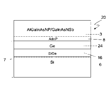
The semiconductor device 20 of figure 3 mainly differs from the embodiment of
figure 2 by the
particular choice of its substrate 7. In this embodiment the Ge layer 24 is
not strain relaxed, but has
a high residual compressive strain and thus a smaller lateral lattice constant
than the strain relaxed
Ge layer 2 of figures 1 and 2.
In order to be able to still grow a multilayer structure 3 onto the substrate
7 an additional strain
compensation layer 8, in this case AllnP is grown onto the Ge layer 24 and the
Ge layer 24 is grown
onto a SiGe layer 16.
In this case in order to be able to grow the multilayer structure 9 on the
substrate 7 it is necessary
to reduce the lattice constant of the material of the inactive layer. For the
embodiment of figure 3
A10.6Ga0.39In0.c1Aso.998N0.001P0.00lhas been chosen.
By use of the SiGe layer 16 between the Si layer 6 and the Ge layer 24 the
lattice constant is
gradually increased from Si towards Ge, wherein the SiGe layer is relaxed
before the Ge layer is
grown on top of it. The Ge composition changes over the thickness of the SiGe
layer 16. However,
the lattice constant does not reach the lattice constant of Ge before the Ge
layer is grown. Conse-
quently, there is residual compressive strain left in the Ge layer 24, which
is compensated by use
of a strain compensation layer 8 of AllnP. All nP has an even smaller lattice
constant than the part
of the SiGe layer 16 in contact with Ge layer 24.
To obtain a successful growth of an AlGaAs material on such structure, one
needs to reduce the
lattice constant of the AlGaAs material of the inactive layer. This can be
done by choosing a proper
composition of AlGalnAsNP ¨ e.g. one could use
A10.6Ga0.391n0.01AS0.949N0.001P0.05, where z and c
are adjusted to reach the desired lattice constant which is smaller than that
of Ge and larger than
that of the strain compensation layer 8.
Figure 4 shows a more detailed view of a semiconductor device following the
design principles of
figure 2.
Again the substrate 5 comprises a Si layer 6 and a strain relaxed Ge layer 2,
wherein a laser
structure 11 is grown onto the substrate 5. In an embodiment not depicted in
the figures the Si layer
6 could well be replaced by a Ge layer.
In the embodiment of figure 5 between the Si layer 6 and a strained Ge layer
24, a SiGe layer 16
is located. Furthermore a strain compensation layer 8 is located between the
Ge layer 24 and the
optoelectronic semiconductor multilayer structure 11. In this embodiment the
substrate 17 is formed
by the Si layer 6, the SiGe layer 16, the Ge layer 24 and the strain
compensation layer 8.
CA 03071711 2020-01-31
WO 2019/052672 PCT/EP2017/073521
- 9 -
The laser structure 11 of figures 4 and 5 comprises a multiple quantum well
structure 12. The
multiple quantum well structure 12 has multiple alternating layers of quantum
well material and a
barrier material. The quantum well material that has smaller bandgap than the
barrier material
forming a potential well (quantum well) for electrons and holes when inserted
between two layers
of barrier material. The multiple quantum well structure 12 is formed by one
or more quantum wells
separated by the barrier material.
The quantum well structure 12 is sandwiched between two waveguide layers 13
both of GalnAs.
The functionality of the GalnAs layers 14 is to act as a waveguide and keep
the optical field confined
in the region of the multi-quantum well structure 12. Those inactive waveguide
layers 13 have a
considerable thickness of up to 3 pm but still do not lead to any substantial
built up of compressive
strain in the structure.
.. In addition the optoelectronic multilayer structure 11 comprises two
cladding layers 14 of A10.6Ga0.4
As. Further on top of the upper cladding layer 14 there is a contact layer 15.
Figure 6 shows a schematic cross-sectional view of an alternative embodiment
of a semiconductor
device 40 according to the present disclosure. On a substrate 5 as it has been
described with
reference to figures 2 and 4 above an optoelectronic semiconductor multilayer
structure 23 has
been grown.
In addition to a multi-quantum well structure 12 embedded between two cladding
layers 14 and an
additional contact layer 15 on top of the structure a distributed Bragg
reflector 18 has been inte-
grated into the multilayer structure 23. Alternative designs of the substrate
5 as they have been
described in detail above could be implemented.
Figure 7 is a graph presenting relative output power in arbitrary units over
test time in hours. The
continuous line in the graph of figure 7 represents the output power of a
comparative structure,
wherein a laser diode has been fabricated on a GaAs substrate. The comparative
structure is sche-
matically depicted in figure 8 b). The relative output power of the
comparative structure decreases
with increasing test time.
The dashed line in the graph of figure 7 represents relative output power of a
semiconductor device
according to the present disclosure comprising a laser diode structured on a
substrate having a Ge
layer. The comparative structure is schematically depicted in figure 8 a). The
relative output power
of the comparative structure is roughly constant over test time.
CA 03071711 2020-01-31
WO 2019/052672 PCT/EP2017/073521
- 10 -
Figure 8 c) shows the Band gap of the optoelectronic multilayer structure of
the laser diodes ac-
cording to figures 8 a) and b).
Figure 9 is a graph plotting the X-ray diffraction signal over the Omega-
2Theta angle of a GaAs
layer grown on Ge substrate. The difference (in arc sec) of the diffraction
peaks is linked to the
lattice mismatch between the GaAs and Ge layers. The mismatch of the AlGaAs
material-based
layers on Ge layer should not exceed this. The strain in of the GaAs layer in
the figure 8 is tensile
meaning that the GaAs peak is on the right side of the Ge peak. However, the
strain of the AIGaAs
on Ge may also be compressive, in which case its diffraction peak would be on
the left side of the
Ge peak, but the distance should still be the same or smaller than the
distance of the GaAs and
Ge peaks.
Figure 10 is a schematic cross-sectional view of a semiconductor device 60
having a microelec-
tronic multilayer semiconductor structure 19 forming a transistor. The
substrate 17 is identical to
the substrate 17 of figure 5. The transistor formed by the semiconductor
multilayer structure 19
comprises a layer 21 of an AlGaAs-based material and a layer 22 consisting of
AlGalnAsNSb. In
order to be able to operate as a transistor the multilayer structure 19
further has contacts 23, 25
acting as the gate, as the drain, and as the source of the transistor,
respectively.
For purposes of original disclosure, it is pointed out that all features which
are apparent for a person
skilled in the art from the present description, the figures and the claims,
even if they have only
been described with further features, could be combined on their own or
together with all the com-
binations of the features disclosed herein, if not excluded explicitly or
technically impossible. A
comprehensive explicit description of all possible combinations of features is
only omitted in order
to provide readability of the description.
While the disclosure has been described with respect to a limited number of
embodiments, it will
be understood that the disclosure is not limited to those embodiments. Other
embodiments com-
prising various changes do not depart from the scope of the disclosure. In
particular, the description
of preferred embodiments shall not be understood to be limited to what is
explicitly shown and
described in the specification and drawings but shall encompass the disclosure
of the specification
and drawings as a whole.
CA 03071711 2020-01-31
WO 2019/052672
PCT/EP2017/073521
- 11 -
Reference numerals
1, 10, 20, 30, 40, 50 optoelectronic semiconductor device
60 microelectronic semiconductor device
2, 24 Ge layer
3, 4, 11, 23 optoelectronic semiconductor multilayer structure
5, 7, 17 substrate
6 Si layer
8 strain compensation layer
12 multiple quantum well structure
13 waveguide layer
14 cladding layer
contact layer
16 SiGe layer
15 18 distributed Bragg reflector
19 microelectronic semiconductor multilayer structure
21 AlGaAs-based layer
22 AlGalnAsNSb layer
source/drain
20 26 gate