Note : Les descriptions sont présentées dans la langue officielle dans laquelle elles ont été soumises.
OFFSET BLOCK WAVEGUIDE COUPLER
TECHNICAL FIELD
The present invention relates generally to waveguides and, more particularly,
to a waveguide coupler that efficiently launches a desired uniform or non-
uniform
Radio Frequency (RF) field-distribution into an open parallel-plate
transmission line
structure.
BACKGROUND ART
Multiple techniques have been employed to couple a waveguide into a
parallel-plate transmission line that is multiple wavelengths in width. These
techniques include, for example, direct open-ended waveguide-to-parallel-plate
interfaces, indirect slot-coupled waveguide-to-parallel-plate interfaces,
direct coax-to-
parallel-plate interfaces, and horn feeds.
Direct open-ended waveguide-to-parallel-plate interfaces tend to be bulky and
have grating-lobe related limits on maximum spacing. They also require
separate
corporate or traveling-wave feed for excitation and can be relatively
expensive and
difficult to realize in practical injection-molded structures. Examples of
direct open-
ended waveguide-to-parallel-plate interfaces include an array of open-ended
rectangular or ridged waveguides (E-plane aligned), and an array of open-ended
rectangular or ridged waveguides (with 90 degree twists).
Indirect slot-coupled waveguide-to-parallel-plate interfaces also are bulky
and
often have limited bandwidth due to the resonant properties of the requisite
coupling
slot. They also are difficult to realize in practical injection-molded
structures. Further,
some grating-lobe limitations exist for maximum spacing and for potential
higher-
order mode excitation in some slot excitation geometries. Examples of indirect
waveguide-to-parallel-plate interfaces include a common-broadwall (series-
series,
shunt-series) coupling.
1
CA 3073382 2020-02-24
Direct coax-to-parallel-plate interfaces are bulky with grating-lobe related
limits
on maximum interelement spacing and require a separate corporate or traveling-
wave feed for excitation.
Horn-feeds, like the other techniques, also are bulky and have limits on
excitation phase and amplitude control.
SUMMARY OF INVENTION
In view of the aforementioned shortcomings of currently available methods for
coupling a waveguide into a parallel-plate transmission line, a device and
method in
accordance with the present invention efficiently feed a desired uniform or
non-
uniform radio frequency (RF) field-distribution into an open parallel-plate
transmission
line. More specifically, controlled coupling of energy is performed via a
centered
continuous slot opening in a wall of the waveguide that connects one or both
broadwall(s) of a rectangular waveguide to an adjoining parallel-plate
transmission
line, where a plurality of stepped sections extend along a length of the
waveguide
and create a controlled coupling through the continuous-centered slot. When
compared to conventional methods, the device and method in accordance with the
invention provide superior excitation control, superior physical compactness,
broader
operating frequency bandwidth capability, enhanced design flexibility, and
superior
tolerance insensitivity/producibility.
According to one aspect of the invention, a waveguide coupler includes: a
waveguide including a first and a second port; a first slot formed in a first
broadwall of
the waveguide between the first and second ports, the first slot centered on
the first
broadwall; a plurality of shifted waveguide sections arranged between the
first and
second ports and extending along a length of the waveguide; and a first
parallel-plate
transmission line structure coupled to the first slot, wherein RF signals
within one of
the waveguide or the parallel-plate transmission line are communicated to the
other
of the waveguide or the parallel-plate transmission line through the slot.
2
CA 3073382 2020-02-24
In one embodiment, each shifted waveguide section includes an alternating
arrangement of ascending or descending steps.
In one embodiment, the alternating arrangement of ascending or descending
steps is formed at least partially on sidewalls of the waveguide, and each
step on a
first sidewall of the waveguide is offset along a length of the waveguide from
a step
on a second sidewall of the waveguide, the second sidewall opposite the first
sidewall.
In one embodiment, each shifted waveguide section comprises at least one
step having a step width and a step height, and each step of the plurality of
shifted
waveguide sections has the same step width and step height as other steps of
the
plurality of shifted waveguide sections.
In one embodiment, each shifted waveguide section comprises at least one
step having a step width and a step height, and at least one step of the
plurality of
shifted waveguide sections has a different step width or step height from
other steps
of the plurality of shifted waveguide sections.
In one embodiment, the step width corresponds to a quarter wavelength of an
RE signal propagating through the waveguide.
In one embodiment, the waveguide a-dimension of the waveguide coupler is
constant throughout.
In one embodiment, the plurality of shifted waveguide sections approximate a
sinusoidal profile in the waveguide coupler.
In one embodiment, the waveguide a-dimension of the waveguide coupler
varies.
In one embodiment, the second port comprises a load that attenuates an RE
signal propagating in the waveguide.
In one embodiment, the second port comprises a short that electrically
connects the first sidewall to the second sidewall.
In one embodiment, the waveguide coupler comprises a dielectric material.
3
CA 3073382 2020-02-24
In one embodiment, the dielectric material comprises one of a solid dielectric
or an air dielectric.
In one embodiment, the waveguide coupler includes a plurality of tuner
features formed in at least one of the first broadwall or a second broadwall
of the
waveguide.
In one embodiment, the tuner features are at least partially formed in at
least
one of the shifted waveguide sections.
In one embodiment, the waveguide coupler includes a second slot formed a
second broadwall of the waveguide, the second broadwall arranged opposite the
first
broadwall.
In one embodiment, the waveguide coupler includes a second parallel-plate
transmission line structure coupled to the second slot to communicate RF
signals
between the waveguide and the parallel plate transmission line.
In one embodiment, each port comprises an electrical short circuit, further
comprising a plurality of input waveguides coupled to a second broadwall of
the
waveguide, wherein at least one shifted waveguide section of the plurality of
shifted
waveguide sections is arranged between adjacent input waveguides.
In one embodiment, virtual shorts are formed at boundaries between adjacent
input waveguides.
According to another aspect of the invention, a method is provided for
launching a desired uniform or non-uniform Radio Frequency (RF) field-
distribution
from a waveguide into an open parallel-plate transmission line structure,
wherein the
waveguide is coupled to the parallel-plate transmission line via a continuous
slot
centered in a broadwall of the waveguide. The method includes using shifted
waveguide sections in the waveguide to perturb the RF field distribution in
such a
way as to couple RF energy via the continuous slot in order to create a
desired e-field
distribution in the parallel-plate section.
4
CA 3073382 2020-02-24
To the accomplishment of the foregoing and related ends, the invention, then,
comprises the features hereinafter fully described and particularly pointed
out in the
claims. The following description and the annexed drawings set forth in detail
certain
illustrative embodiments of the invention. These embodiments are indicative,
however, of but a few of the various ways in which the principles of the
invention may
be employed. Other objects, advantages and novel features of the invention
will
become apparent from the following detailed description of the invention when
considered in conjunction with the drawings.
BRIEF DESCRIPTION OF DRAWINGS
In the annexed drawings, like references indicate like parts or features.
Figs. 1A and 1B are schematic diagrams of equivalent circuits for shifted
waveguide sections in accordance with the invention.
Fig. 2 illustrates an exemplary antenna system that utilizes a waveguide
coupler in accordance with the present invention.
Figs. 3A and 3B are side and perspective views of a parallel-plate fed (single-
sided) basic shifted waveguide section Feed.
Figs. 4A and 4B are side and perspective views of a modified shifted
waveguide section variant with dissimilar length blocks on opposing sides of
the
rectangular waveguide.
Figs.5A and 5B are side and perspective views of a modified shifted
waveguide section variant with added broadwall tuners in order to "match"
IS111=0
(useful for efficient broadside operation with traveling-wave designs.)
Fig. 6 is a perspective view of a basic or modified shifted waveguide section
with dual-sided parallel-plate coupling into two opposing parallel-plate
regions via two
slots in the two opposing rectangular waveguide broadwalls.
Fig. 7A-7B are side and perspective views of a basic (or modified) (M)OSB
variant realized as an "N-Element" standing-wave feed and fed via individual
discrete
5
CA 3073382 2020-02-24
waveguide ports connecting the broadwall of the waveguide opposite the
broadwall
coupling to the parallel-plate.
DETAILED DESCRIPTION OF INVENTION
For RE antenna applications it is desirable to create controlled amplitude and
phase distributions ("aperture excitations") in order to meet specific antenna
gain,
sidelobe, beamwidth, and overall antenna pattern ("RE radiation") design
characteristics. For direct-radiating array antennas employing parallel-plate
transmission lines, this implies the need for efficient launching (from a
single
waveguide interface, the "input/output" port of the antenna) of controlled
transverse
electric (TE) parallel-plate waveguide "modes" that are bounded and
propagating
within the parallel-plate structure.
As used herein, a parallel-plate transmission line is defined as an RF
transmission line that includes two generally parallel conductive plates (two
or more
wavelengths in width and one or more wavelengths in length) separated by a
predetermined distance (generally less than% wavelength) from one another.
In a conventional waveguide feed, a linear array of discrete resonant slots
are
offset various distances from a center line of the common broadwall of a
waveguide
(line-feed) in order to provide the desired coupling characteristic
(individual slot
coupling values) such that a specific phase and amplitude distribution (and
requisite
power-to-load) is realized. Such conventional device exhibits limited
bandwidth
capability, largely due to the classical (undesirable) variation in "real" (G)
and
"reactive" (jB) coupling components of the resonant coupling slots as
operating
frequency moves away from the design center frequency (fo).
In contrast, the device and method in accordance with the present invention
employ novel periodic or pseudo-periodic waveguide sidewall and broadwall
features
incorporated into a single straight rectangular waveguide "feed" adjoining the
parallel-
plate transmission line. A pseudo-periodic waveguide is generally within 10
percent
of a strictly periodic structure, i.e., features are separated from one
another by a fixed
6
CA 3073382 2020-02-24
distance or by a distance that varies within 10 percent of a fixed distance.
The
features excite ("launch") desired parallel-plate modes consistent with
realization of a
desired aperture excitation and thereby the desired RF antenna
characteristics.
Further, the device and method in accordance with the invention employ a
continuous centered slot along the broadwall centerline of the waveguide line-
feed,
forming a (reduced height) intermediate parallel-plate region (e.g., a "fin")
which is
subsequently coupled/transitioned into a (increased height) parallel-plate
transmission-line section.
In its simplest basic "offset block" (OSB) embodiment (also referred to as a
shifted waveguide embodiment), the sidewalls of the waveguide are "offset" as
constant-width "blocks" (waveguide sections) in order to control local
coupling from
the waveguide line feed into the parallel-plate region. These shifted
waveguide
sections are typically one-quarter guide-wavelength in length and
longitudinally
separated by one-half guide wavelength (inter-element spacing), with
individual
shifted waveguide sections alternating in offset direction in synchronicity
with the
internal waveguide fields (broadwall current patterns) associated with the
dominant
TE10 propagating modes.
Referring initially to Fig. 1A, a simplified equivalent circuit is shown with
the
coupled power (coupled from the waveguide into the parallel-plate) represented
as a
shunt conductance (G) and the reflections and phase shift associated with RF
fringing at each edge of the shifted waveguide section represented as shunt
inductances, each offset 1/8 of a wavelength from the centerline of the
section.
As a result of the individual shifted waveguide section's (typical) %-
wavelength, the reactive components at leading and lagging edges cancel
leaving
(predominantly at "resonance") a matched pseudo-constant coupling (modeled via
the shunt conductance) as a function of waveguide offset. Referring to Fig.
1B, a
more generalized equivalent circuit model for the individual shifted waveguide
is a
shunt admittance (Y) with short transmission-line sections of length d' on
either end
in order to "model" the phase-shift associated with the inductive fringing at
the abrupt
shifted waveguide transitions. Resonance is defined as when the shunt
admittance
7
CA 3073382 2020-02-24
is pure real, the insertion phase (unlike a typical slot) has residual
positive phase
component (as modeled by the short transmission line sections).
With reference to Fig. 2, illustrated is an exemplary system 2 implementing
waveguide coupler 10 in accordance with the present invention. In addition to
the
waveguide coupler 10, the system 2 includes a parallel-plate transmission line
4
communicatively connected to the coupler 10, and an antenna array 6 (e.g., a
continuous transverse stub (CTS) array) coupled to the parallel-plate
transmission
line 4. RF signals enter the waveguide coupler 10 via a waveguide input 10a,
are
communicated to the parallel-plate transmission line 4 and radiated by the
antenna
array 6.
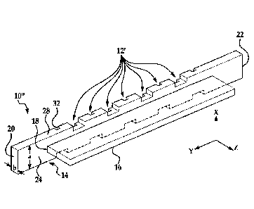
Referring now to Figs. 3A and 3B, illustrated are side and perspective views
of
an exemplary waveguide coupler 10 in accordance with a first embodiment of the
present invention. The basic design employs identical-length shifted waveguide
sections 12 down the length of a rectangular waveguide 14. As used herein, a
"shifted waveguide section" refers to at least one step change (ascending or
descending) in a sidewall of the waveguide resulting in a shift of the
waveguide
centerline in that section that is approximately 1/4 wavelength in length. As
seen in
Figs. 3A and 3B, alternating 1/4-wave shifted waveguide sections 12
excite/couple
rectangular waveguide fields into a parallel-plate 16 via a slot/fin 18
extending from
the center of the broadwall of the rectangular waveguide 14.
The rectangular waveguide 14 includes a first input/output (I/O) port 20 and a
second I/O port 22, wherein one or both of the first and second I/O ports may
receive
RF signals. As will be described in more detail below, in one embodiment one
I/O
port is configured to receive an RF signal and the other I/O port is
configured to
absorb (attenuate) the RF signal, i.e., it acts as a load. In another
embodiment both
I/O ports receive an RF signal, and in yet another embodiment both I/O ports
are
configured as electrical short circuits.
The slot 18 is formed in a first broadwall 24 of the waveguide 14 between the
first and second I/O ports 20, 22. The slot 18, which preferably is centered
on the
8
CA 3073382 2020-02-24
first broadwall 24, is approximately equal in length and width and coupled to
the
parallel-plate transmission line 16, which receives and/or provides RF signals
from/to
the waveguide 14. Between the shifted waveguide sections 12 are a plurality of
unshifted waveguide sections 26 arranged between the first and second I/O
ports 20,
22 and extend along a length of the waveguide 14.
Alternating shifted waveguide sections 12 are of equal step length, and can be
formed by stepping each sidewall 28. In the embodiment of Figs. 3A-3B, the
shifted
waveguide sections 12 are complementary to each other, i.e., the equal steps
in the
same direction relative to the waveguide 14 centerline effectively shift the
waveguide
centerline in the shifted waveguide section. This results in a waveguide a-
dimension
and b-dimension of the shifted waveguide sections as being the same as the a-
dimension and b-dimension of the unshifted waveguide sections but with their
centerlines offset from one another. As shown in Figs. 3A-3B, each shifted
waveguide section includes an alternating arrangement of ascending or
descending
steps that approximate a sinusoidal profile in the waveguide coupler.
In the embodiment shown in Figs. 3A and 3B, each shifted waveguide section
12 includes a step having a step width and a step height, and each step of the
plurality of shifted waveguide sections has the same step width and step
height as
other steps of the plurality of shifted waveguide sections. In another
embodiment, at
least one step of the plurality of shifted waveguide sections has a different
step width
or step height from other steps of the plurality of shifted waveguide
sections. The
dimensions of each step can be configured to provide a desired characteristic.
For
example, a first step width may correspond to a quarter wavelength of an RF
signal
at one particular operating frequency propagating through the waveguide and a
second step width may correspond to a quarter wavelength of the RF signal at a
second particular operating frequency to provide a desired coupling
characteristic
between the waveguide and the parallel-plate transmission line (e.g., the
reflections
at each step will cancel out, each at slightly different frequencies).
When compared to the closest "relative" (e.g., a traveling-wave fed waveguide
employing series-series/angle-slots or shunt-series offset slots), the device
in
9
CA 3073382 2020-02-24
accordance with the present invention is better-suited for injection molding.
This is
due at least in part to the use of a continuous centered slot (coupling from
the
waveguide centerline to the parallel-plate) together with sidewall shifted
waveguide
sections or "meander" features, which can be realized in a simple two-piece
mold. In
other words, internal details or resonant slots are not required, thereby
simplifying the
mold. Additionally, high-Q resonant structures are not present, which results
in wider
operating frequency bandwidth (unlike the behavior of typical resonant
coupling
structures, the equivalent slot conductance "G" of the device and method
according
to the invention is largely frequency independent). Further, the device and
method in
accordance with the invention provide superior tolerance insensitivity as
compared to
"conventional" high-Q structures. This provides high-performance even at
millimeter
wave (MMVV) frequencies (through 94 GHz) using conventional injection-molding
techniques.
Also, superior bandwidth performance of the device and method in
accordance with the invention enables traveling-wave implementations with
"radiating
load" (e.g., the last coupling unshifted waveguide section(s) is/are employed
as a
termination load for the traveling-wave feed, thereby eliminating the need for
a
conventional load, and eliminating the associated efficiency loss). The
bilateral and
balanced nature of the coupling mechanism also allows for both one-sided
(launch in
one parallel-plate direction) and two-sided (launch in two opposing parallel-
plate
directions) implementations.
In a variant of the basic design, referred to as the "Modified Offset Block
(MOSB)" feed 10' (or modified shifted waveguide feed) and shown in Figs. 4A-
4B,
the abrupt steps (of equal length on both opposing sides of the waveguide) are
replaced by a single step on just one side of the waveguide to form each
alternating
shifted waveguide section, thereby creating the discretized "meandering" of
the
waveguide centerline on either side of the centered broadwall slot ( or "fin",
which is
applicable in cases where a dielectric medium is a solid material instead of
air)
between unshifted waveguide sections 26. In this embodiment the single-step
shifted waveguide sections maximize the operating bandwidth of the MOSB
structure
CA 3073382 2020-02-24
despite having a smaller a-dimension as compared to the unshifted waveguide
sections. The MOSB has generally wider bandwidth characteristics as compared
to
the OSB, based on the reduction of the "abrupt" waveguide section offset
steps,
thereby removing one of the resonant (bandwidth-limiting) characteristics. The
equivalent circuits for both variants are similar.
As illustrated in Figs. 4A and 4B, the waveguide coupler 10' is similar to
that
shown in Figs. 3A-3B, with the exception of the arrangement of the shifted
waveguide
sections 12', where only a single sidewall step is employed to achieve the
shifting of
the waveguide centerline in the shifted waveguide sections. As can be seen in
Figs.
4A-4B, between the shifted waveguide sections 12' are a plurality of unshifted
waveguide sections 26 arranged between the first and second I/O ports 20, 22
and
extend along a length of the waveguide 14. In contrast to the waveguide
coupler 10
of Figs. 3A-3B, a cross section of the waveguide coupler 10' through sidewalls
of the
waveguide 14 is not constant and instead varies along a length of the
waveguide.
This variant provides similar microwave characteristics to the basic
(identical section
length) but has the mechanical advantage of allowing for a narrower overall
cross-
section.
In terms of design limitations for the embodiment of Figs. 4A and 4B, care
should be taken to limit the "b" dimension of the (M)OSB waveguide in order to
limit
the waveguide to single indices (transverse only) waveguide modes. Further,
the
maximum offset together with the waveguide "a" dimension should be limited in
order
to ensure (pre)dominant TE10 waveguide propagation (thoughTE20 is strongly
excited as an evanescent component.) Also, the "b" dimension of the centered
continuous coupling slot should also be constrained in order to minimize
undesired
higher-order (evanescent) mode coupling from the waveguide to the parallel-
plate
region. As used herein, the "a" dimension refers to the longer dimension of
the
waveguide cross-section (the broadwall height) and the "b" dimension refers to
the
shorter dimension of the waveguide cross-section (the sidewall).
Moving now to Figs. 5A-5B, illustrated is a waveguide coupler 10" in
accordance with another embodiment of the invention. The embodiment of Figs.
5A-
11
CA 3073382 2020-02-24
5B is similar to the embodiment of Figs. 4A-4B, but includes tuner features 32
formed
in at least one of the first (front) broadwall or a second (rear/opposing)
broadwall of
the waveguide 14. The broadwall tuner features, which in the exemplary
embodiment are formed as rectangular grooves formed in a broadwall and
spanning
between opposing sidewalls, are configured to "match" IS111=0. This is useful
for
efficient broadside operation with traveling-wave designs wherein the
undesirable
peak in input reflection coefficient (due to coherent addition of the
reflections of
individual elements) is largely mitigated. The tuner features 32 can be formed
in
portions of the broadwall 24 and/or sidewall 28 that do not include a shifted
waveguide section 12', or they can at least partially be formed in a shifted
waveguide
section 12', as can be seen in Fig. 5B. Alternative embodiments may employ
tuner
features having semicircular features instead of rectangular grooves
Referring now to Fig. 6, illustrated is a dual-sided waveguide coupler 10"
coupling into two opposing parallel-plate transmission lines 16, 16a in
accordance
with another embodiment of the invention. The embodiment of Fig. 6 is similar
to the
embodiment of Figs. 3A and 3B but includes a second slot 18a formed in the
second
(opposing) broadwall 24a of the waveguide 14'. The second parallel-plate
transmission line 16a is coupled to the second slot 18a to communicate RF
signals
between the waveguide 14' and the parallel plate transmission line 16a. The
embodiment of Fig. 6 is advantageous in that signals from the waveguide 14'
can be
selectively split into one of the two transmission line structures 16, 16a
and/or
received from each of the transmission line structures and combined in the
waveguide 14'.
Moving to Figs. 7A and 7B, illustrated is a waveguide coupler 10" in
accordance with another embodiment of the invention. The waveguide coupler 10"
is similar to the waveguide coupler 10 of Figs. 3A and 3B, but is realized as
an "N-
Element" standing-wave feed and fed via a plurality of individual discrete
rectangular
waveguide ports 40 connected to the rear broadwall 24a (i.e., the broadwall
opposite
the broadwall 24 coupled to the parallel-plate transmission line 16). As seen
in Figs.
7A and 7B, at least one shifted waveguide section 12 of the plurality of
shifted
12
CA 3073382 2020-02-24
waveguide sections is arranged between adjacent input waveguides 40. Further,
each I/O port 20, 22 includes an electrical short circuit between opposing
sidewalls.
The short circuit may be formed, for example, by including a metal conductor
or the
like connecting the opposing sidewalls. Due to boundary conditions imposed on
opposing waveguide signals, virtual short-circuits are naturally realized at
the
boundaries between opposing waveguide fed sections. As a signal enters the
waveguide coupler 10" from waveguide ports 40, it splits in in both directions
and
travels along the waveguide, where it resonates between the short circuit at
one port
and the virtual short (or between virtual shorts ¨ see the unit cell in Fig.
7A) before
exiting via the slot and into the parallel-plate transmission line 16.
The waveguide couplers described herein can be realized as an air-filled, or
more typically, a single dielectric-filled waveguide structure. This reduces
the
size/thickness of the assembly and further simplifies low-cost injection-
molding as an
integrated structure (one-piece fabrication including OSB feed and radiating
CTS
structure). In the air-filled embodiment, the waveguide may be formed from a
plastic
or like material to define the respective portions of the waveguide coupler,
and a
metallized surface can be formed on or in the plastic material. In the
dielectric
embodiment, a metalized surface can be formed over the dielectric material.
Also,
the structures can be terminated in a conventional load or a traveling-wave
fed
structure can be terminated in a "coupling/zero-loss" load, where the last
coupling
element(s) are employed as a "radiating" load thereby eliminating the
undesired loss
associated with conventional absorptive loads.
The device and method in accordance with the invention departs from the
conventional methods described herein by coupling the propagating energy
inside
the rectangular waveguide through a long centered narrow slot on its broadwall
where it is transitioned into the parallel-plate (see Fig. 3A). This is an
improved
derivative of the conventional longitudinal offset slot waveguide feed
employing an
array of discrete (resonant) slots.
Potential benefitting applications include (but are not limited to) Continuous
Transverse Stubs (CTS) and Variable Inclination Continuous Transverse Stub
13
CA 3073382 2020-02-24
(VICTS) antennas or any other microwave device employing parallel-plate
transmission line structure(s.)
Although the invention has been shown and described with respect to a
certain embodiment or embodiments, equivalent alterations and modifications
may
occur to others skilled in the art upon the reading and understanding of this
specification and the annexed drawings. In particular regard to the various
functions
performed by the above described elements (components, assemblies, devices,
compositions, etc.), the terms (including a reference to a "means") used to
describe
such elements are intended to correspond, unless otherwise indicated, to any
element which performs the specified function of the described element (i.e.,
that is
functionally equivalent), even though not structurally equivalent to the
disclosed
structure which performs the function in the herein exemplary embodiment or
embodiments of the invention. In addition, while a particular feature of the
invention
may have been described above with respect to only one or more of several
embodiments, such feature may be combined with one or more other features of
the
other embodiments, as may be desired and advantageous for any given or
particular
application.
14
CA 3073382 2020-02-24