Note : Les descriptions sont présentées dans la langue officielle dans laquelle elles ont été soumises.
CA 03074728 2020-03-04
PROCESSES FOR PRODUCING ELECTRO-OPTIC DISPLAYS
[Para 1] This application is related to U.S. Patents Nos. 6,982,178;
7,561,324; and
7,839,564.
[Para 21 This invention relates to processes for producing electro-optic
displays. More
specifically, this invention relates to processes for the production of
electro-optic displays
without the use of front plane laminates, inverted front plane laminates and
double release films
as described in the aforementioned U.S. Patents Nos. 6,982,178; 7,561,324; and
7,839,564, and
to processes for depositing encapsulated electrophoretic media by spraying.
[Para 3] The term "electro-optic", as applied to a material or a display, is
used herein in its
conventional meaning in the imaging art to refer to a material having first
and second display
states differing in at least one optical property, the material being changed
from its first to its
second display state by application of an electric field to the material.
Although the optical
property is typically color perceptible to the human eye, it may be another
optical property,
such as optical transmission, reflectance, luminescence or, in the case of
displays intended for
machine reading, pseudo-color in the sense of a change in reflectance of
electromagnetic
wavelengths outside the visible range.
[Para 4] The term "gray state" is used herein in its conventional meaning in
the imaging art
to refer to a state intermediate two extreme optical states of a pixel, and
does not necessarily
imply a black-white transition between these two extreme states. The term
"monochrome" may
be used hereinafter to denote a drive scheme which only drives pixels to their
two extreme
optical states with no intervening gray states.
[Para 5] Some electro-optic materials are solid in the sense that the
materials have solid
external surfaces, although the materials may, and often do, have internal
liquid- or gas-filled
spaces. Such displays using solid electro-optic materials may hereinafter for
convenience be
referred to as "solid electro-optic displays". Thus, the term "solid electro-
optic displays"
includes rotating bichromal member displays, encapsulated electrophoretic
displays, microcell
electrophoretic displays and encapsulated liquid crystal displays.
[Para 6] The terms "bistable" and "bistability" are used herein in their
conventional meaning
in the art to refer to displays comprising display elements having first and
second display states
differing in at least one optical property, and such that after any given
element has been driven,
by means of an addressing pulse of finite duration, to assume either its first
or second display
state, after the addressing pulse has terminated, that state will persist for
at least several times,
for example at least four times, the minimum duration of the addressing pulse
required to
-1-
CA 03074728 2020-03-04
WO 2019/089042 PCT/1JS2017/059887
change the state of the display element. It is shown in U.S. Patent No.
7,170,670 that some
particle-based electrophoretic displays capable of gray scale are stable not
only in their extreme
black and white states but also in their intermediate gray states, and the
same is true of some
other types of electro-optic displays. This type of display is properly called
"multi-stable" rather
than bistable, although for convenience the term "bistable" may be used herein
to cover both
bistable and multi-stable displays.
I Para 71 Several types of electro-optic displays are known, for example
(a) a rotating bichromal member type as described, for example, in U.S.
Patents
Nos. 5,808,783; 5,777,782; 5,760,761; 6,054,071 6,055,091; 6,097,531;
6,128,124;
6,137,467; and 6,147,791;
(b) an electrochromic medium, for example an electrochromic medium in the
form
of a nanochromic film comprising an electrode formed at least in part from a
semi-
conducting metal oxide and a plurality of dye molecules capable of reversible
color
change attached to the electrode; see, for example U.S. Patents Nos.
6,301,038;
6,870,657; and 6,950,220; and
(c) an electro-wetting display as described in Hayes, R.A., et al., "Video-
Speed
Electronic Paper Based on Electrowefting", Nature, 425, 383-385 (2003) and
U.S.
Patent No. 7,420,549.
[Para 81 One type of electro-optic display, which has been the subject of
intense research
and development for a number of years, is the particle-based electrophoretic
display, in which
a plurality of charged particles move through a fluid under the influence of
an electric field.
Electrophoretic displays can have attributes of good brightness and contrast,
wide viewing
angles, state bistability, and low power consumption when compared with liquid
crystal
displays. Nevertheless, problems with the long-term image quality of these
displays have
prevented their widespread usage. For example, particles that make up
electrophoretic displays
tend to settle, resulting in inadequate service-life for these displays.
[Para 9] As noted above, electrophoretic media require the presence of a
fluid. In most prior
art electrophoretic media, this fluid is a liquid, but electrophoretic media
can be produced using
gaseous fluids; see, for example, Kitamura, T., et al., "Electrical toner
movement for electronic
paper-like display", IIDW Japan, 2001, Paper HCS1-1, and Yamaguchi, Y., et
al., "Toner
display using insulative particles charged triboelectrically", IDW Japan,
2001, Paper AMD4-
4). See also U.S. Patents Nos. 7,321,459 and 7,236,291. Such gas-based
electrophoretic media
appear to be susceptible to the same types of problems due to particle
settling as liquid-based
-2-
CA 03074728 2020-03-04
WO 2019/089042 PCT/1182017/059887
electrophoretic media, when the media are used in an orientation which permits
such settling,
for example in a sign where the medium is disposed in a vertical plane.
Indeed, particle settling
appears to be a more serious problem in gas-based electrophoretic media than
in liquid-based
ones, since the lower viscosity of gaseous suspending fluids as compared with
liquid ones
allows more rapid settling of the electrophoretic particles.
[Pam 101 Numerous patents and applications assigned to or in the names of the
Massachusetts
Institute of Technology (MIT) and E Ink Corporation describe various
technologies used in
encapsulated electrophoretic and other electro-optic media. Such encapsulated
media comprise
numerous small capsules, each of which itself comprises an internal phase
containing
electrophoretically-mobile particles in a fluid medium, and a capsule wall
surrounding the
internal phase. Typically, the capsules are themselves held within a polymeric
binder to form
a coherent layer positioned between two electrodes. The technologies described
in these patents
and applications include:
(a) Electrophoretic particles, fluids and fluid additives; see for
example U.S. Patents Nos. 7,002,728; and 7,679,814;
(b) Capsules, binders and encapsulation processes; see for example
U.S. Patents Nos. 6,922,276; and 7,411,719;
(c) Films and sub-assemblies containing electro-optic materials; see
for example U.S. Patents Nos. 6,825,829; 6,982,178; 7,236,292; 7,443,571;
7,513,813; 7,561,324; 7,636,191; 7,649,666; 7,728,811; 7,729,039; 7,791,782;
7,839,564; 7,843,621; 7,843,624; 8,034,209; 8,068,272; 8,077,381; 8,177,942;
8,390,301; 8,482,852; 8,786,929; 8,830,553; 8,854,721; and 9,075,280; and
U.S. Patent Applications Publication Nos. 2009/0109519; 2009/0168067;
2011/0164301; 2014/0027044; 2014/0115884; and 2014/0340738;
(d) Backplanes, adhesive layers and other auxiliary layers and
methods used in displays; see for example U.S. Patents Nos. D485,294;
6,124,851; 6,130,773; 6,177,921; 6,232,950; 6,252,564; 6,312,304; 6,312,971;
6,376,828; 6,392,786; 6,413,790; 6,422,687; 6,445,374; 6,480,182; 6,498,114;
6,506,438; 6,518,949; 6,521,489; 6,535,197; 6,545,291; 6,639,578; 6,657,772;
6,664,944; 6,680,725; 6,683,333; 6,724,519; 6,750,473; 6,816,147; 6,819,471;
6,825,068; 6,831,769; 6,842,167; 6,842,279; 6,842,657; 6,865,010; 6,967,640;
6,980,196; 7,012,735; 7,030,412; 7,075,703; 7,106,296; 7,110,163; 7,116,318;
7,148,128; 7,167,155; 7,173,752; 7,176,880; 7,190,008; 7,206,119; 7,223,672;
-3-
CA 03074728 2020-03-04
WO 2019/089042 PCT/1JS2017/059887
7,230,751; 7,256,766; 7,259,744; 7,280,094; 7,327,511; 7,349,148; 7,352,353;
7,365,394; 7,365,733; 7,382,363; 7,388,572; 7,442,587; 7,492,497; 7,535,624;
7,551,346; 7,554,712; 7,583,427; 7,598,173; 7,605,799; 7,636,191; 7,649,674;
7,667,886; 7,672,040; 7,688,497; 7,733,335; 7,785,988; 7,843,626; 7,859,637;
7,893,435; 7,898,717; 7,957,053; 7,986,450; 8,009,344; 8,027,081; 8,049,947:
8,077,141; 8,089,453; 8,208,193; 8,373,211; 8,389,381; 8,498,042; 8,610,988;
8,728,266; 8,754,859; 8,830,560; 8,891,155; 8,989,886; 9,152,003; and
9,152,004; and U.S. Patent Applications Publication Nos. 2002/0060321;
2004/0105036; 2005/0122306; 2005/0122563; 2007/0052757; 2007/0097489;
2007/0109219; 2009/0122389; 2009/0315044; 2011/0026101; 2011/0140744;
2011/0187683; 2011/0187689; 2011/0292319; 2013/0278900; 2014/0078024;
2014/0139501; 2014/0300837; 2015/0171112; 2015/0205178; 2015/0226986;
2015/0227018; 2015/0228666; and 2015/0261057; and International
Application Publication No. WO 00/38000; European Patents Nos. 1,099,207
Bland 1,145,072B1;
(e) Color formation and color adjustment; see for example
U.S.
Patents Nos. 7,075,502; and 7,839,564;
(t) Methods for driving displays; see for example U.S.
Patents Nos.
7,012,600; and 7,453,445;
(g) Applications of displays; see for example U.S. Patents Nos.
7,312,784; and 8,009,348; and
(h) Non-electrophoretic displays, as described in U.S. Patents Nos.
6,241,921; 6,950,220; 7,420,549; 8,319,759; and 8,994,705; and U.S. Patent
Application Publication No. 2012/0293858.
[Para 111 Many of the aforementioned patents and applications recognize that
the walls
surrounding the discrete microcapsules in an encapsulated electrophoretic
medium could be
replaced by a continuous phase, thus producing a so-called polymer-dispersed
electrophoretic
display, in which the electrophoretic medium comprises a plurality of discrete
droplets of an
electrophoretic fluid and a continuous phase of a polymeric material, and that
the discrete
droplets of electrophoretic fluid within such a polymer-dispersed
electrophoretic display may
be regarded as capsules or microcapsules even though no discrete capsule
membrane is
associated with each individual droplet; see for example, the aforementioned
U.S. Patent No.
-4-
CA 03074728 2020-03-04
WO 2019/089042 PCT/1JS2017/059887
6,866,760. Accordingly, for purposes of the present application, such polymer-
dispersed
electrophoretic media are regarded as sub-species of encapsulated
electrophoretic media.
[Para 121 Although electrophoretic media are often opaque (since, for example,
in many
electrophoretic media, the particles substantially block transmission of
visible light through the
display) and operate in a reflective mode, many electrophoretic displays can
be made to operate
in a so-called "shutter mode" in which one display state is substantially
opaque and one is light-
transmissive. See, for example, U.S. Patents Nos. 5,872,552; 6,130,774;
6,144,361; 6,172,798;
6,271,823; 6,225,971; and 6,184,856. Dielectrophoretic displays, which are
similar to
electrophoretic displays but rely upon variations in electric field strength,
can operate in a
similar mode; see U.S. Patent No. 4,418,346. Other types of electro-optic
displays may also be
capable of operating in shutter mode. Electro-optic media operating in shutter
mode may be
useful in multi-layer structures for full color displays; in such structures,
at least one layer
adjacent the viewing surface of the display operates in shutter mode to expose
or conceal a
second layer more distant from the viewing surface.
[Para 131 An encapsulated electrophoretic display typically does not suffer
from the
clustering and settling failure mode of traditional electrophoretic devices
and provides further
advantages, such as the ability to print or coat the display on a wide variety
of flexible and rigid
substrates. (Use of the word "printing" is intended to include all forms of
printing and coating,
including, but without limitation: pre-metered coatings such as patch die
coating, slot or
extrusion coating, slide or cascade coating, curtain coating; roll coating
such as knife over roll
coating, forward and reverse roll coating; gravure coating; dip coating; spray
coating; meniscus
coating; spin coating; brush coating; air knife coating; silk screen printing
processes;
electrostatic printing processes; thermal printing processes; ink jet printing
processes;
electrophoretic deposition (See U.S. Patent No. 7,339,715); and other similar
techniques.)
Thus, the resulting display can be flexible. Further, because the display
medium can be printed
(using a variety of methods), the display itself can be made inexpensively.
[Para 141 Other types of electxo-optic materials may also be used in the
present invention.
[Para 151 The aforementioned U.S. Patent No. 6,982,178 describes a method of
assembling a
solid electro-optic display (including an encapsulated electrophoretic
display) which is well
adapted for mass production. Essentially, this patent describes a so-called
"front plane
laminate" ("FPL") which comprises, in order, a light-transmissive electrically-
conductive
layer; a layer of a solid electro-optic medium in electrical contact with the
electrically-
conductive layer; an adhesive layer, and a release sheet. Typically, the light-
transmissive
-5-
CA 03074728 2020-03-04
WO 2019/089042 PCT/1JS2017/059887
electrically-conductive layer will be carried on a light-transmissive
substrate, which is
preferably flexible, in the sense that the substrate can be manually wrapped
around a drum
(say) 10 inches (254 mm) in diameter without permanent deformation. The term
"light-
transmissive" is used in this patent and herein to mean that the layer thus
designated transmits
sufficient light to enable an observer, looking through that layer, to observe
the change in
display states of the electro-optic medium, which will normally be viewed
through the
electrically-conductive layer and adjacent substrate (if present); in cases
where the electro-
optic medium displays a change in reflectivity at non-visible wavelengths, the
term "light-
transmissive" should of course be interpreted to refer to transmission of the
relevant non-visible
wavelengths. The substrate will typically be a polymeric film, and will
normally have a
thickness in the range of about 1 to about 25 mil (25 to 634 gm), preferably
about 2 to about
mil (51 to 254 pm). The electrically-conductive layer is conveniently a thin
metal or metal
oxide layer of, for example, aluminum or ITO, or may be a conductive polymer.
Poly(ethylene
terephthalate) (PET) films coated with aluminum or ITO are available
commercially, for
example as "aluminized Mylar" ("Mylar" is a Registered Trade Mark) from ET. du
Pont de
Nemours & Company, Wilmington DE, and such commercial materials may be used
with good
results in the front plane laminate.
[Para 161 Assembly of an electro-optic display using such a front plane
laminate may be
effected by removing the release sheet from the front plane laminate and
contacting the
adhesive layer with the backplane under conditions effective to cause the
adhesive layer to
adhere to the backplane, thereby securing the adhesive layer, layer of electro-
optic medium and
electrically-conductive layer to the backplane. This process is well-adapted
to mass production
since the front plane laminate may be mass produced, typically using roll-to-
roll coating
techniques, and then cut into pieces of any size needed for use with specific
backplanes.
[Para 171 The aforementioned U.S. Patent No. 7,561,324 describes a so-called
"double
release sheet" which is essentially a simplified version of the front plane
laminate of the
aforementioned U.S. Patent No. 6,982,178. One form of the double release sheet
comprises a
layer of a solid electro-optic medium sandwiched between two adhesive layers,
one or both of
the adhesive layers being covered by a release sheet. Another form of the
double release sheet
comprises a layer of a solid electro-optic medium sandwiched between two
release sheets. Both
forms of the double release film are intended for use in a process generally
similar to the
process for assembling an electro-optic display from a front plane laminate
already described,
but involving two separate laminations; typically, in a first lamination the
double release sheet
-6-
CA 03074728 2020-03-04
WO 2019/089042 PCT/1JS2017/059887
is laminated to a front electrode to form a front sub-assembly, and then in a
second lamination
the front sub-assembly is laminated to a backplane to form the fmal display,
although the order
of these two laminations could be reversed if desired.
[Para 181 The aforementioned U. S. Patent No. 7,839,564 describes a so-called
"inverted front
plane laminate", which is a variant of the front plane laminate described in
the aforementioned
U.S. Patent No. 6,982,178. This inverted front plane laminate comprises, in
order, at least one
of a light-transmissive protective layer and a light-transmissive electrically-
conductive layer;
an adhesive layer, a layer of a solid electro-optic medium; and a release
sheet. This inverted
front plane laminate is used to form an electro-optic display having a layer
of lamination
adhesive between the electro-optic layer and the front electrode or front
substrate; a second,
typically thin layer of adhesive may or may not be present between the electro-
optic layer and
a backplane. Such electro-optic displays can combine good resolution with good
low
temperature performance.
[Para 19] As already indicated, the aforementioned front plane laminates,
inverted front plane
laminates and double release films are well adapted for production by roll-to-
roll processes,
thus producing the front plane laminate, inverted front plane laminate or
double release film in
the form of a roll of material which can be severed into pieces of the size
needed for individual
displays and laminated to appropriate backplanes. However, also as already
indicated, to effect
the necessary lamination, and layer of lamination adhesive normally needs to
be present
between the electro-optic layer itself and the backplane, and this layer of
lamination adhesive
remains in the final display between the two electrodes. The presence of this
lamination
adhesive layer has significant effects on the electio-optic properties of the
display. Inevitably,
some of the voltage drop between the electrodes occurs within the lamination
adhesive layer,
thus reducing the voltage available for driving the electro-optic layer. The
effect of the
lamination adhesive tends to become greater at lower temperatures, and this
variation in the
effect of lamination adhesive with temperature complicates the driving of the
display. The
voltage drop within the lamination adhesive can be reduced, and the low
temperature operation
of the display improved, by increasing the conductivity of the lamination
adhesive layer, for
example by doping the layer with tetrabutylammonium hexafluorophosphate or
other materials
as described in U.S. Patents Nos. 7,012,735 and 7,173,752. However, increasing
the
conductivity of the lamination adhesive layer in this manner tends to increase
pixel blooming
(a phenomenon whereby the area of the electro-optic layer which changes
optical state in
response to change of voltage at a pixel electrode is larger than the pixel
electrode itself), and
-7-
CA 03074728 2020-03-04
WO 2019/089042 PCT/1JS2017/059887
this blooming tends to reduce the resolution of the display. Hence, this type
of display
apparently intrinsically requires a compromise between low temperature
performance and
display resolution.
[Para 201 One aspect of the present invention relates to processes for the
production of
electro-optic displays which do not require the presence of a lamination
adhesive layer between
the electro-optic layer and the backplane; these processes involve coating the
electio-optic
material on to the backplane.
[Para 211 A second aspect of the present invention relates to novel processes
for application
of encapsulated electrophoretic media to substrates. These processes may be
used to aid in the
first aspect of the invention but may also be used in other types of coating
processes.
[Para 22] The electrophoretic media described in the aforementioned E Ink
patents and
applications, and similar prior art electrophoretic media typically comprise
electrophoretic
particles, charge control agents, image stability agents and flocculants in a
non-polar liquid,
typically encapsulated in a flexible organic matrix such as a gelatin/acacia
coacervate. To
produce commercial displays, it is necessary to coat a thin layer (preferably
a monolayer ¨ see
U.S. Patent No. 6,839,158) of capsules on a substrate, which may be a front
substrate bearing
an electrode (see the aforementioned U.S. Patent No. 6,982,178), a backplane
or a release sheet.
Hitherto, coating of encapsulated electrophoretic media on substrates has
typically been
effected by slot coating, in which a slurry of capsules in a carrier medium is
forced through a
slot on to a substrate which is moving relative to the slot. Slot coating
imposes limitations upon
the viscosity and other physical properties of the material being coated and
typically requires
the addition of slot coating additives to control the rheology of the coated
material to ensure
that the coating does not flow and develop non-uniformities in thickness prior
to drying. Thus,
in slot coating electrophoretic capsules are typically supplied in the form of
aqueous slurries
containing optional latex binder, rheology modification agents, ionic dopants,
and surfactants.
These additives remain in the final dried electrophoretic medium and may
affect its properties,
including its electro-optic properties.
[Para 231 Furthermore, although slot coating is well adapted for applying
electrophoretic
media to continuous webs, it is not well adapted for "patch" coating of
discrete areas of a web
or discrete parts (for example, individual backplanes) lying on a moving belt,
since settling and
self-segregation of capsule slurry within the slot die manifold become
problematic during such
"interrupted" capsule deposition processes. Slot coating is generally not
useful for non-planar
substrates, which is unfortunate since encapsulated electrophoretic media are
well adapted for
-8-
CA 03074728 2020-03-04
WO 2019/089042 PCT/1JS2017/059887
coating three-dimensional objects, including architectural features. Other
problems with slot
coating include chatter-like streaks parallel to the coating slot die (these
streaks are believed to
result from periodic bunching or jamming of capsules), and streaking in the
direction of coating
(believed to be due to capsule jamming or non-uniform flows in delivery of
capsules to the slot
coating slot die).
[Pam 241 The aforementioned problems with slot coating have resulted in a
search for an
alternative coating technology able to cope with patch coating and coating of
non-planar
substrates, as well as planar objects and webs. One well established coating
technology which
has been considered for this purpose is spray coating, i.e., the pneumatic
atomization and
deposition of capsule dispersions. Spray coating is a mature technology, but
prior art attempts
to apply the technology to capsule deposition have been subject to various
defects and modes
of failure. Because they typically have flexible capsule walls, capsules
deform and sometime
rupture during spraying, either during the atomization step or upon impact on
the target. The
consequences of significant capsule rupture, including the release of
electrophoretic particles,
fluid etc., are so severe that, so far as the present inventors are aware,
unacceptable levels of
ruptured capsules have by themselves been sufficient to doom all previous
attempts to spray
coat encapsulated electrophoretic media. The second aspect of the present
invention provides
a spray coating process which reduces or eliminates these problems.
[Para 251 A third aspect of the present invention relates to processes for
reducing the adhesion
of capsules to a substrate during coating in order to facilitate close packing
of capsules on the
substrate. This adhesion reduction process is primarily intended for use with
spray coating of
capsules but may also be useful with other capsule deposition techniques.
[Para 261 As previously mentioned, in the production of electrophoretic
displays it is
generally preferred to form a monolayer of capsules on a substrate. However, a
common
problem encountered when coating electrophoretic capsules on to a substrate
(typically a
ITO/PET film, a PET/release film, or any type of silicone release film) is
that the capsules
adhere strongly to the substrate and are unable to rearrange themselves into
an optimally packed
monolayer upon drying. Various coating materials have been found to
significantly reduce
capsule-substrate adhesion, thus allowing the capsules to rearrange themselves
by means of
capillary forces during drying. Unfortunately, if such coating materials are
used in slot coating
processes employing a doctor blade, as is common during slot coating, the
reduced capsule-
substrate adhesion causes the capsules to not pass properly past the doctor
blade; instead, the
vast majority of the capsules are simply pushed in front of the doctor blade,
leaving only a very
-9-
CA 03074728 2020-03-04
WO 2019/089042 PCT/1JS2017/059887
sparse capsule coating on the substrate. Accordingly, there is a need for an
improved process
for the formation of closely packed monolayers of capsules on substrates, and
the third aspect
of the present invention seeks to provide such a process.
[Para 271 A fourth aspect of the present invention relates to processes for
overcoating electro-
optic materials to planarize an electro-optic layer and/or adhere the electro-
optic layer to a
transparent front electrode that may be attached to a color filter.
I Para 28.1 It is known (see especially United States Patent No. 7,839,564)
that a color display
may be formed by overlaying a color filter array (CFA) over an monochromatic
black/white
electro-optic display, with the CFA elements aligned with the pixel electrodes
of the backplane.
Such a CFA may for example have repeating red, green and blue stripes, or a
repeating 2 x 2
red/green/blue/white (clear) pixel pattern. The brightest state of such a
display is achieved
when all pixels of the electro-optic layer are white, and it is therefore
preferred that the
absorption of the CFA elements, taken as a whole, be constant across the
visible range, so that
the brightest state will have no color tint.
[Pam 291 Overlaying a CFA over an electro-optic layer in this manner leads to
a trade-off
between brightness and color saturation, and the colors that are most
difficult to render are the
brightest colors, such as white and yellow. Moreover, such a display suffers
from several
sources of light loss or contamination that limit still further the quality of
color attainable.
These include:
(a) absorption of light by the white state of the electro-optic layer that
limits
the brightness of all colors; this may be as much as 50% of light incident on
a
white region of the electro-optic layer;
(b) reflection of light by the dark state of the electro-optic layer,
causing
pollution of a desired color by unwanted light of other colors;
(c) contrast at the pixel level ("local contrast") may be lower than the
contrast measured if the entire display is switched from the white state to
the
dark state, due to electrical effects at the edges of pixels (i.e., image
"blooming")
or to optical effects related to the scattering length within the electro-
optic layer
(i.e., "optical dot gain");
(d) loss of light due to total internal reflection within the display;
since
electrophoretic and most other reflective electro-optic layer are Lambertian
reflectors, a significant proportion of light may be reflected at angles to
the
-10-
CA 03074728 2020-03-04
WO 2019/089042 PCT/1182017/059887
normal greater than the critical angle for total internal reflection at at
least one
surface between adjacent layers of the display and be lost;
(e) illumination parallax: if the CFA elements are significantly separated
from the electro-optic layer by intervening layers, light incident on the
display
at sufficiently large angles to the normal may pass through a color filter
element
of one color and exit the display through an element of a different color,
leading
to pollution of the colored image and a color shift; and
(f) viewing parallax: for the same reasons as in (e), if a viewer observes
the
display at a sufficiently large angle to the normal, and the CFA elements are
significantly separated from the electro-optic layer, the viewer may see
modulation of reflectivity through an unintended color filter element.
[Pam 301 When an electro-optic display is formed using a front plane laminate,
as described
above with reference to U.S. Patent No. 6,982,178, a single adhesive layer is
present between
the electro-optic layer and the backplane. Although this adhesive layer is not
disposed between
the electro-optic layer and the CFA (and thus does not contribute to most of
the problems
discussed above), it is present between the electrodes of the display, and
thus contributes to
image blooming. The presence of this adhesive layer also diminishes the
voltage drop actually
occurring across the electro-optic layer, which tends to limit the
reflectivity of the white state
of the electro-optic layer and its contrast ratio. When an electro-optic
display is formed using
either a double release film, as described above with reference to U.S. Patent
No. 7,561,324,
or an inverted front plane laminate, as described above with reference to U.S.
Patent No.
7,839,564, typically two adhesive layers will be present, the first between
the CFA and the
electro-optic layer, and the second between the electro-optic layer and the
bacicplane. The
second adhesive layer contributes to the same problems as the adhesive layer
derived from an
FPL, as already discussed; the first adhesive layer at least contributes to
the illumination and
viewing parallax problems, and may also contribute to the total internal
reflection problem.
[Para 311 There is thus a need for a process for producing electro-optic
displays which reduces
or eliminates the problems caused by the presence of adhesive layers between
the electrodes.
However, since as discussed above, manufacture of electro-optic displays
necessitates at least
one lamination operation, the best process will involve the provision of only
one thin adhesive
layer, and the present invention seeks to provide such a process.
[Pam 321 Accordingly, in one aspect this invention provides a process for
producing a sub-
assembly for use in an electro-optic display, the process comprising:
-11-
CA 03074728 2020-03-04
WO 2019/089042 PCT/1JS2017/059887
providing a backplane comprising at least one electrode located in a first
area
of the backplane;
covering a second area of the backplane spaced from the electrode with a
masking layer,
coating the backplane having the masking layer thereon with a layer of an
electro-optic material; and
removing the masking layer, and the portion of the layer of electro-optic
medium thereon, from the backplane, thereby producing a sub-assembly
comprising the
backplane having its first area covered by the layer of electro-optic material
but its second area
free from the layer of electro-optic material.
[Para 33] This process may hereinafter for convenience be referred to as the
"masked
backplane" process of the invention. In one form of this process, the second
area of the
backplane comprises a contact pad intended, in the final display, to make
electrical contact with
the front electrode of the display. In this form of the invention, a light-
transmissive conductive
layer may be partially covered with a lamination adhesive, and laminated to
the
backplane/electro-optic material sub-assembly with the lamination adhesive
contacting the
electro-optic material and the light-transmissive conductive layer in
electrical contact with the
contact on the backplane. This electrical contact may be direct, or may be
made via an
electrically conductive ink or similar deformable conductive material.
[Pam 34] In another form of the process, after the layer of electro-optic
material has been
coated on the backplane, but before the masking layer is removed, a layer of
lamination
adhesive (preferably a 100 per cent solids radiation-curable adhesive) is
coated over the electio-
optic material, and then the masking layer is removed, together with both the
portions of the
layers of electro-optic material and the lamination adhesive thereon. A light-
transmissive
electrically-conductive layer can then be laminated to the lamination adhesive
in the first area
of the backplane; the light-transmissive electrically-conductive layer
preferably extends into
the second area of the backplane so as to make electrical contact with the
contact pad in this
second area.
[Para 351 In a further form of the process, the backplane has a third area
which is covered by
a second masking layer which can be removed separately from the (first)
masking layer
covering the second area. In this form of the process, after the layer of
electro-optic material
has been coated, the second masking layer is removed, thus exposing the third
area of the
backplane. A light-transmissive electrically-conductive layer is now coated
over the backplane.
-12-
CA 03074728 2020-03-04
[Para 361 In a second aspect, this invention provides a process for spraying
capsules of an
electrophoretic medium on to a substrate, the process comprising:
forming a dispersion of the capsules in a liquid;
feeding the dispersion through a first orifice; and
feeding a continuous stream of gas through a second, annular orifice
surrounding
the first orifice, thereby forming a spray of the capsules. During spraying of
the capsules, a
masking material covers part of the substrate, and after the spraying the
masking
material and the capsules thereon are removed so that, after removal of the
masking material,
capsules remain only on those portions of the substrate where the masking
material was not
present.
[Para 37] This process may hereinafter for convenience be referred to as the
"spray coating
process" of the present invention. The process may include shaping the spray
by feeding a
continuous stream of gas through a plurality of shaping orifices disposed
adjacent the spray. The
spray may be directed on to any type of substrate, including a web, a
plurality of discrete objects
disposed on a support or one or more three-dimensional (i.e., non-planar)
objects. If, as is
typically the case, the capsule walls are formed from a hydrophilic material
(such as the
aforementioned gelatin/acacia coacervate), the liquid used to disperse the
capsules is desirably
aqueous; depending upon the specific capsules and liquid used, the liquid may
optionally
comprise any one or more of pH modifiers, surfactants and ionic dopants. The
gas passed
through both the second orifice and the shaping orifices is typically air, but
it some cases it may
be useful to use an inert gas, for example nitrogen.
[Para 38] The spray coating process of the present invention may include the
use of a masking
material covering part of the substrate so that, after removal of the masking
material, capsules
remain only on those portions of the substrate where the masking material was
not present. Such
a "masked spray coating process" of the invention may comprise multiple steps
with each step
involving the use of a different mask and a different capsule dispersion so
that the different
capsule dispersions are disposed in different areas of the final display.
[Para 39] In a third aspect, this invention provides a process for forming a
monolayer of
capsules on a substrate, the process comprising:
depositing a solution of a water-swellable polymer on the substrate; and
-13-
= CA 03074728 2020-03-04
thereafter depositing a quantity of the capsules sufficient to form a
monolayer of
capsules on to the substrate, and allowing the capsules to arrange themselves
into a
monolayer on the substrate.
[Para 40] This process may hereinafter for convenience be referred to as the
"swellable polymer
coating process" of the present invention. The polymer used may be, for
example, a
polysaccharide, such as a pectin, or a protein, especially an albumin. The
albumin used may be,
for example, egg albumin or bovine serum albumin; other types of albumin may
also be
-13a-
CA 03074728 2020-03-04
WO 2019/089042 PCT/1JS2017/059887
suitable. At least when the capsules are formed of a hydrophilic material
(such as the
gelatin/acacia coacervate mentioned in many of the E Ink patents and
applications mentioned
above), the polymer solution is preferably an aqueous solution. The deposition
of the capsules
is desirably effected by a process such as spray coating which does not
require contact of a
coating head or coating bar with the capsule layer.
[Pam 411 In a fourth aspect, this invention provides a process for forming an
electio-optic
display, the process comprising:
providing a backplane comprising at least one electrode;
coating the backplane with a layer of an electro-optic material;
depositing a layer of a substantially solvent-free polymerizable liquid
material
over the layer of electro-optic material;
contacting the polymerizable liquid material with at least one light-
transmissive
electrically-conductive layer; and
exposing the polymerizable liquid material to conditions effective to cause
polymerization of the material, thereby adhering the at least one light-
transmissive electrically-conductive layer to the layer of electro-optic
material.
!Para 421 This process may hereinafter for convenience be referred to as the
"overcoat layer
process" of the present invention. In this process, the coating of the
backplane with the electro-
optic material may be conducted by the masked backplane process of the present
invention (to
permit masking of any areas, for example row and column electrodes, which
should not be
covered by electro-optic material) and/or by the spray coating process of the
present invention.
[Para 431 In one form of the overcoat layer process of the present invention,
both a light-
transmissive electrically-conductive layer and a color filter array are
adhered to the electro-
optic layer. Typically, the light-transmissive electrically-conductive layer
is mounted on a front
substrate, which is provided with a color filter array (which may be printed
directly on to the
front substrate). The front substrate may serve to provide mechanical support
to the electrically-
conductive layer, many conductive layers, for example indium-tin-oxide (ITO)
layers are too
fragile to be self-supporting.
[Para 441 In a second form of the overcoat layer process of the present
invention, the electro-
optic layer is a color electro-optic layer capable of displaying a variety of
colors (a so-called
"inherent color" layer), and only a front plane electrode (and any supporting
substrate required)
are adhered to the electro-optic layer by means of the polymerizable liquid
material.
-14-
CA 03074728 2020-03-04
WO 2019/089042 PCT/1JS2017/059887
[Para 45] Figure 1 of the accompanying drawings is a schematic top plan view
of a backplane
undergoing a first masked backplane process of the present invention.
Para 461 Figure 2A is a schematic section along line 2A-2A in Figure 1 but
showing the
backplane after deposition of electro-optic material thereon.
[Para 47] Figure 2B is a schematic section similar to that of Figure 2A but
showing the
backplane after the masking layer has been removed.
'Pam 481 Figure 2C is a schematic section through a sub-assembly comprising a
light-
transmissive, electrically-conductive layer and a layer of lamination
adhesive.
[Pam 491 Figure 2D is a schematic section similar to those of Figures 2A and
2B but showing
the backplane after lamination of a front electrode and front substrate to the
electro-optic
material via a layer of lamination adhesive.
[Pam 501 Figure 3A is a schematic section similar to that of Figure 2A but
showing the same
stage in a second masked backplane process of the present invention.
[Para 51] Figure 3B is a schematic section similar to those of Figures 2B and
3A but showing
the backplane after formation of a layer of lamination adhesive overlying the
electro-optic
material but before removal of the masking layer.
[Para 52] Figure 3C is a schematic section similar to that of Figure 3B but
showing the
backplane after removal of the masking layer.
[Para 53] Figure 3D is a schematic section similar to that of Figures 2D and
3C but showing
the backplane after lamination of a front electrode and front substrate to the
electm-optic
material via the layer of lamination adhesive.
[Para 541 Figure 4A is a schematic section similar to those of Figures 2A and
3A but showing
the same stage in a third masked backplane process of the present invention
which uses two
separate masking layers.
[Para 551 Figure 4B is a schematic section similar to that of Figure 4A but
showing the
backplane after removal of the second masking layer.
[Para 561 Figure 4C is a schematic section similar to those of Figures 4A and
4B but showing
the backplane after formation of a light-transmissive front electrode layer
overlying the electro-
optic material.
I Para 57) Figure 4D is a schematic section similar to those of Figures 4A-4C
but showing the
backplane after removal of the first masking layer.
-15-
CA 03074728 2020-03-04
WO 2019/089042 PCT/1JS2017/059887
[Para 58] Figure 5 is a schematic top plan view, similar to that of Figure 1,
of the backplane
used in the third masked backplane process after application of the two
masking layers but
before deposition of the electro-optic layer.
[Para 59] Figure 6 is a schematic cross-section through a simple spray coating
nozzle used in
the spray coating process of the present invention.
[Para 60] Figure 7 is a cross-section through a more complex spray coating
nozzle used in the
spray coating process of the present invention.
[Para 61] Figure 8 is an enlarged view of the portion of the nozzle lying
within the dotted box
in Figure 7.
[Para 621 Figure 9 is a graph illustrating preferred parameters used in the
spray coating
process of the present invention.
[Para 63] Figure 10 is a top plan view of a first electrophoretic display
produced by a masked
spray coating process of the present invention.
[Pam 64] Figure 11 is a top plan view of a second electrophoretic display
produced by a
masked spray coating process of the present invention.
[Pam 65] Figures 12A-12H are time lapse micrographs showing an experimental
demonstration of the swellable polymer coating process of the present
invention using capsules
deposited from a pipette on to a microscope slide.
[Para 661 Figure 13 is a schematic cross-section through a prior art color
display using a color
filter array and produced using a double release film as previously described.
Para 671 Figure 14 is a schematic cross-section similar to that of Figure 13
but taken through
a color display produced by the overcoat layer process of the present
invention.
[Para 68] Figure 15 is a schematic cross-section similar to those of Figures
13 and 14 through
a prior art inherent color display.
[Para 691 Figure 16 is a schematic cross-section similar to those of Figures
13 to 15 but taken
through an inherent color display produced by the overcoat layer process of
the present
invention.
[Para 701 As already indicated, this invention has several different aspects,
which will
primarily be described separately below. However, it should be appreciated
that a single
physical process may make use of more than one aspect of the invention. Thus,
for example, a
masked backplane process of the invention might make use of the air spray
coating process of
the invention to deposit electro-optic material on a backplane treated by the
swellable coating
-16-
CA 03074728 2020-03-04
WO 2019/089042 PCT/1JS2017/059887
process of the invention, and the layer of electro-optic material might
thereafter be treated by
the overcoat layer process of the invention.
I Para 711 Masked backplane process
[ Para 721 As indicated above, the masked backplane process of the present
invention provides
a process for producing a sub-assembly for use in an electro-optic display.
This process
comprises providing a backplane comprising at least one electrode located in a
first area of the
backplane; covering a second area of the backplane spaced from the electrode
with a masking
layer; coating the backplane having the masking layer thereon with a layer of
an electro-optic
material; and removing the masking layer, and the portion of the layer of
electro-optic medium
thereon, from the backplane, thereby producing a sub-assembly comprising the
backplane
having its first area covered by the layer of electro-optic material but its
second area free from
the layer of electro-optic material. Thus, the masked backplane process allows
for formation
of a sub-assembly, and ultimately an electro-optic display, without the use of
a pre-formed front
plane laminate and without the presence of a lamination adhesive layer between
the electro-
optic layer and the backplane, thus reducing or eliminating the problems
associated with this
lamination adhesive layer, as discussed above.
'Para 73] The masked backplane process of the present invention builds the sub-
assembly or
display starting from the backplane. The process may be carried out on
individual backplanes
but for mass production purposes it is more conveniently effected on
backplanes arranged in a
multi-up configuration. Conceptually, when used to produce a complete display,
the masked
backplane process may be regarded as involving (a) the backplane itself, which
may be a
segmented, passive matrix or active matrix backplane; (b) a masking layer for
protecting areas
of the backplane which are not be covered by the electro-optic material (the
protected areas
will typically be those required for making a "top plane connection" to the
front electrode of
the final display, and may also include areas used for conductors leading to
the pixel electrodes
and electronic components such as row and column drivers); (c) a solid electro-
optic medium,
typically an encapsulated electrophoretic medium; (d) a light-transmissive,
electrically-
conductive layer which forms the front electrode of the display; and (e) a
means, typically a
lamination adhesive, for securing the light-transmissive, electrically-
conductive layer to the
solid electro-optic medium.
[Para 741 As already indicated, the backplane used in the masked backplane
process may be
of any known type, although care should be taken to ensure that the backplane
used does not
damage the electro-optic layer. For example if the electro-optic layer is to
be formed from an
-17-
CA 03074728 2020-03-04
WO 2019/089042 PCT/1JS2017/059887
encapsulated electrophoretic medium, the backplane should not have such sharp
changes in
level as to risk puncturing some of the capsules. The masking layer may be
formed from a
simple polymeric film which adheres to the backplane either because of its own
physical
properties or with the aid of an adhesive coating, but should desirably not be
more than about
75 pm in thickness; polymeric films which have been found useful as masking
layers include
Kapton tape (a polyimide tape available from du Pont de Nemours & Company,
Wilmington,
DE) and RP301 film (an acrylic film available form Nitto America, Inc.,
Fremont CA). The
solid electro-optic layer is typically an encapsulated electrophoretic layer
but may also be a
polymer-dispersed electrophoretic layer or a rotating bichromal member or
electrochromic
layer. Care should be taken to ensure that the physical properties of the
electro-optic layer are
such that the portions of the layer overlying the masking layer are removed
when the masking
layer itself is removed, without tearing the masking layer so that portions of
the masking layer
are left on the backplane and/or without portions of the electro-optic layer
in the unmasked
portion of the backplane being inadvertently removed. The material used to
form the front
electrode and the adhesive can be any of the materials used in the prior art
for this purpose.
[Para 751 Specific masked backplane processes of the invention will now be
described in
more detail with reference to Figures 1 to 4 of the accompanying drawings.
Figure 1 is a top
plan view of an active matrix backplane (generally designated 100) having a
first, central area
102 provided with a two dimensional array of pixel electrodes (not shown), and
a second,
peripheral area 104 covered by a masking film 106. (It will be appreciated
that the relative sizes
and dispositions of the first and second areas 102 and 104 can vary widely and
it is not
necessary that the second area 104 surround the first area 102.) The second
area 104 will
normally include a contact pad for making electrical contact with a front
electrode (described
below) and may include row and column electrodes connected to the pixel
electrodes in the
first area 102 and sockets for row and column drivers.
[Para 761 After provision of the masking layer on the backplane, the next step
of the masked
backplane process is coating the backplane with a layer of electro-optic
material 108, as
illustrated in Figure 2A. Any technique capable of depositing the layer of
electro-optic material
on the backplane may be used to form layer 108; with an encapsulated
electrophoretic electro-
optic material, slot die coating, bar coating and spray coating methods have
all been
successfully used to apply the electrophoretic material directly to a masked
backplane.
Depending upon the deposition method used, the layer of electro-optic material
may or may
-18-
CA 03074728 2020-03-04
WO 2019/089042 PCT/1JS2017/059887
not cover completely both the first and second areas of the backplane; for
example, some spray
coating methods may only coat part of the masked area.
[Para 771 The next step of the process is removal of the masking layer 106 to
expose the
second area 104 of the backplane 100, and the electrical connectors and/or
sockets thereon, as
illustrated in Figure 2B. As already noted, it is important to choose the
masking layer and the
electro-optic material such that the masking film and overlying layer of
electro-optic material
are removed completely from the second area 104 but that no portion of the
electro-optic
material overlying the first area 102 is removed.
[Pam 781 To complete the assembly of an electro-optic display, it is necessary
to secure a
light-transmissive, electrically conductive layer over the layer of electro-
optic material 108. As
shown in Figure 2C, this is most conveniently effected by providing a front
substrate 110
carrying the light-transmissive, electrically conductive layer or front
electrode layer 112. As
discussed for example in the aforementioned U.S. Patent No. 6,982,178,
polymeric films
coated with indium tin oxide ([TO) are available commercially and are very
suitable for
providing the front substrate 110 and front electrode layer 112. A layer of
lamination adhesive
114 is then formed on the front electrode layer 112, leaving exposed a portion
of the front
electrode layer 112 needed to provide an electrical connection to the
backplane 100. In practice,
it is generally most convenient to coat the whole of the front electrode layer
112 with the
lamination adhesive layer 114 using a roll-to-roll process, cut the resultant
roll into portions of
the size needed for individual displays, and then to remove or "clean" the
lamination adhesive
from the portion of the front electrode layer 112 required to provide the
electrical connection.
A variety of methods for cleaning the lamination adhesive from the requisite
portion of the
front electrode layer 112 are known in the art; see, for example, U.S. Patent
No. 7,733,554.
[Para 791 The sub-assembly shown in Figure 2C is then laminated to the sub-
assembly shown
in Figure 2C with the lamination adhesive layer 114 in contact with the
electro-optic layer 108
to form the final display shown in Figure 2D. Typically, a conductive ink or
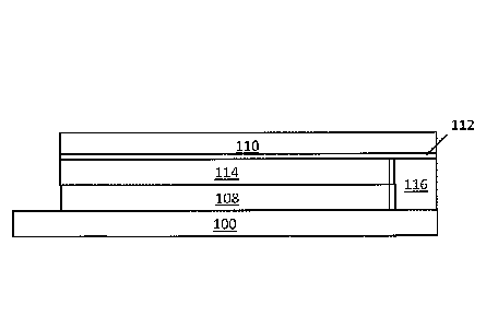
similar material
116 is placed on the backplane 100 adjacent the portion of the front electrode
layer 112 not
covered by the adhesive layer 114, as described in the aforementioned U.S.
Patent No.
6,982,178. This final display has the advantage that the electro-optic layer
108 is in direct
contact with the backplane 100 (without any intervening adhesive layer),
thereby maximizing
the resolution of the display. In addition, the positioning of the adhesive
layer 114 adjacent the
front electrode layer 112 allows the adhesive layer 114 to be made highly
conductive without
detriment to the resolution of the display.
-19-
CA 03074728 2020-03-04
WO 2019/089042 PCT/1.182017/059887
[Para 801 Figures 3A-3D illustrate a second masked backplane process of the
invention in
which an adhesive layer is formed overlying the electro-optic layer before the
masking layer is
removed. The first stages of this second process, namely the provision of a
masking layer 106
on a backplane 100 and the deposition of an electro-optic layer 108 over the
backplane, are
identical to the first process described above, and result in the sub-assembly
shown in Figure
3A, which is essentially identical to that shown in Figure 2A. However, the
next step in the
second process is the coating of a 100 per cent solids radiation-curable
adhesive layer 214 over
the electro-optic layer 108, to produce the structure shown in Figure 3B. The
adhesive layer
214 is left uncured at this step of the process. The masking layer 106 is next
removed, as shown
in Figure 3C, thereby removing the portions of both the electro-optic layer
108 and the adhesive
layer 214 previously overlying the masking layer 106. Again, it is important
to choose the
masking layer, the electro-optic material and the adhesive such that the
masking film and
overlying layers of electro-optic material and adhesive are removed completely
from the
second area 104 but that no portion of the electro-optic material overlying
the first area 102 is
removed.
[Para 811 The final step in the second process is the lamination of a film
comprising a front
substrate 110 and front electrode layer 112 to the sub-assembly shown in
Figure 3C to produce
the final display shown in Figure 3D, with the provision of conductive ink 116
or similar
conductive material as described above with reference to Figure 2D. Since the
radiation-curable
adhesive layer 214 is already present in the sub-assembly of Figure 3C, no
further adhesive is
needed and the front substrate 110 and front electrode layer 112 can be
laminated at
substantially room temperature and without the use of high pressure. The use
of the 100%
solids adhesive layer 214 allows the front electrode layer 112 and front
substrate 110 to take a
variety of forms including flexible substrates and also rigid substrates like
glass. Once the front
electrode layer 112 and front substrate 110 have been applied, the adhesive
layer 214 can be
radiation cured with ultraviolet radiation to produce the final display shown
in Figure 3D. This
display, like that shown in Figure 2D, has the advantage that the electro-
optic layer 108 is in
direct contact with the backplane 100 to maximize the resolution of the
display. In addition, the
positioning of the adhesive layer 214 adjacent the front electrode layer 112
allows the adhesive
layer 214 to be made highly conductive without detriment to the resolution of
the display. The
process of Figures 3A-3D eliminates the top plane cleaning used in the process
of Figures 2A-
2D, allows for a thinner adhesive layer because this layer is applied as a
liquid, allows for
-20-
CA 03074728 2020-03-04
WO 2019/089042 PCT/I1S2017/059887
flexible or rigid front electrode layers and eliminates the need for a high
temperature lamination
step.
[Para 821 Figures 4A-4D illustrate a third masked backplane process of the
invention in which
two separate masking layers are used and a front electrode layer is formed
directly on the
electro-optic layer. The first stages of this third process, namely the
provision of two separate
masking layers 106A and 106B on a backplane 100 and the deposition of an
electro-optic layer
108 over the backplane, are generally similar to the first and second
processes described above,
and result in the sub-assembly shown in Figure 4A, which is generally similar
to those shown
in Figures 2A and 3A except for the provision of the two separate masking
layers 106A and
106B. Masking layer 106A covers the bonding areas for the driver electronics
and edge seal
areas, while masking layer 106B covers the area for front electrode
connection(s). The two
masking layers do not have to be separate films but can be in the form of a
single film cut to
allow two portions thereof to be removed separately, as illustrated
schematically in Figure 5.
Alternatively, depending upon the geometry of the areas covered by the first
and second
masking films, the first masking film may cover all areas of the backplane
which are not to
have electro-optic material deposited thereon, and the second masking film may
be a separate
film applied over the first masking film. The masking films previously
described can be used.
The masked backplane shown in Figure 5 then has electro-optic material
deposited thereon by
any of the methods previously described to produce the structure shown in
Figure 4A.
I Para 831 The next step in the second process is removal of the second
masking layer 106B
without removing the first masking layer 106A, thus exposing the areas of the
backplane
needed for front electrode contacts, and producing the structure shown in
Figure 4B. Next, a
light-transmissive, electrically-conductive front electrode layer 312 is
deposited (normally by
a wet coating process) over the backplane to produce the structure shown in
Figure 4C. The
front electrode layer 312 not only forms a front electrode over the electro-
optic layer 108 but
also forms a front electrode connection with the exposed areas of the
backplane, as illustrated
at the right hand side of Figure 4C. The front electrode layer 312 may be
formed from a
conductive polymer, for example poly(3,4-ethylenedioxythiophene) ("PEDOT"),
normally
used in the form of its poly(styrenesulfonate) salt ("PEDOT:PSS") or a
polyaniline, or may be
formed from network of conductors, for example carbon nanotubes or nanowires.
The present
inventors have successfully coated both PEDOT and carbon nanotube front
electrodes directly
on an encapsulated electrophoretic layer.
-21-
CA 03074728 2020-03-04
WO 2019/089042 PCT/1JS2017/059887
[Para 841 The final step of the process is removal of the first masking layer
106A, together
with the overlying portions of the electro-optic layer 108 and the front
conductor layer 312 to
produce the display illustrated in Figure 4D. If desired driver electronics
and/or edge seals may
now be placed in the exposed areas of the backplane.
[Para 851 The display shown in Figure 4D, like those shown in Figures 2D and
3D, has the
advantage that the electro-optic layer is in direct contact with the
backplane, thus maximizing
the resolution of the display. However, in contrast to the displays described
above, the display
shown in Figure 4D has no lamination adhesive between its electrodes, thus
completely
eliminating the electrical effect of such adhesive. Thus, the display
structure shown in Figure
4D enables the highest resolution and temperature performance for a given
electro-optic layer.
One potential practical problem with the display structure shown in Figure 4D
is that any pore
or pinhole in the electro-optic layer would allow the coated front electrode
to come into
electrical contact with the pixel electrodes on the backplane, thus shorting
the display.
(Para 86i From the foregoing, it will be seen that the masked backplane
process of the present
invention can provide high resolution addressing without compromising
temperature
performance, thus removing the limitations imposed by prior art display
construction methods
which require a thin adhesive between the electro-optic layer and the
backplane. Additionally
the masked backplane process opens up the possibility of conducting the entire
manufacturing
process in a single fab.
[Para 87] Spray coating process
[Para 881 As already mentioned, this invention also provides a process for
spraying capsules
of an electrophoretic medium on to a substrate. This process comprises forming
a dispersion
of the capsules in a liquid; feeding the dispersion through a first orifice;
and feeding a
continuous stream of gas through a second, annular orifice surrounding the
first orifice, thereby
forming a spray of the capsules. This spray coating process has the advantage
over slot coating
that spray coating normally does not require the use of Theology modifiers in
the liquid being
sprayed, so that the final coating is free from such rheology modifiers and
hence free from the
effects such rheology modifiers may have upon the properties of slot coated
electrophoretic
media. Typically, in spray coating, only the additives actually needed in the
final product need
be added to the liquid being sprayed.
[Para 891 Figure 6 is a schematic cross-section through a simple spray coating
nozzle
(generally designated 600) which may be used in the spray coating process of
the present
invention. The nozzle 600 comprises a substantially cylindrical body 602
having a central, axial
-22-
CA 03074728 2020-03-04
WO 2019/089042 PCT11LS2017/059887
bore 604 through which is pumped electrophoretic capsules (not shown)
dispersed in a liquid
(also not shown). The central bore 604 is surrounded by an annular bore 606,
through which is
forced a continuous stream of air. The lower end of the central bore 604
terminates in an orifice
608, which the lower end of the annular bore 606 terminates in an annular
orifice 610, which
surrounds orifice 608. A cylindrical baffle 612 surrounds the annular orifice
610. The air flow
through the annular orifice 610 constrained by the baffle 612 causes the
dispersion of capsules
passing through orifice 608 to form a spray or jet 614.
[Para 901 The nozzle 600 is also provided with shaping air bores 616, which
may be six or
eight in number. As shown in Figure 6, the peripheral portions of the nozzle
600, through which
the bores 616 pass, extend downwardly below the orifices 608 and 610 and the
baffle 612, and
the lower portions of the bores 616 are directly downwardly and inwardly.
Shaping air is forced
continuously through the bores 616 so that it impinges on the jet 614, thereby
causing the jet
to open out into a wide spray 618, which impinges on a substrate 620 disposed
below the nozzle
600.
[Pam 911 Figures 7 and 8 illustrate a high-volume low-pressure atomization
nozzle (generally
designated 700) suitable for use in a high volume spray coating process of the
present invention.
it will be appreciated that in use the nozzle 700 would normally be inverted
relative to the
position illustrated in Figures 7 and 8 so that capsules emerging from the
nozzle would be
directed downwardly on to a substrate, as illustrated in Figure 6.
[Para 921 As will readily be apparent to those familiar with spray nozzle
technology, the
nozzle 700 shown in Figures 7 and 8 operates in substantially the same manner
as the nozzle
600 shown in Figure 6 but the nozzle 700 has the following structural
differences:
(a) the central axial bore 702, through which the capsule dispersion
passes,
tapers adjacent its orifice 708 to increase the velocity at which the capsule
dispersion passes through this orifice;
(b) the simple annular bore 606 in Figure 6 is replaced by a combination of
air feed passage 706A, a cylindrical air plenum 706B, a conical tapering
portion
706C and an outlet portion 706D (Figure 8) which terminates in an annular
orifice 710; in addition, auxiliary shaping air jets are provided by bores
706E
which extend from the tapering portion 706C to orifices on either side of the
orifice 708; and
(c) the shaping air bores 716 are provided with double outlet portions
716A,
716B to provide greater control of the shape of the final capsule spray.
-23-
CA 03074728 2020-03-04
WO 2019/089042 PCT/1JS2017/059887
[Para 93] Figure 8 shows four dimensions which have been found important in
achieving
good spray coating results from the nozzle 700 shown in Figures 7 and 8, these
four dimensions
being (A) the radius of the central orifice 708; (B) the radial distance
between the outer edge
of the central orifice 708 and the inner edge of the annular orifice 706D; (C)
the radial width
of the annular orifice 706D; and (D) the axial distance between the orifices
708 and 710.
[Para 941 The quality of capsules coatings is assessed in terms of their
reproducibility
granularity, mean coating weight, uniformity and defect density; defect
density is quantified by
the number of non-switching capsules per unit display area in a standard
display structure,
which for present purposes is defined as a backplane bearing, in order, a 25
gm layer of
lamination adhesive, a 20 gm capsule layer and a front substrate comprising an
ITO layer on
25 gm polyethylene terephthalate film. The first factor to be considered in
achieving good
spray coatings is capsule and gas flow rates and pressures. It has been found
empirically that
capsule spraying is best achieved using a high-volume, low-pressure ("HVLP")
nozzle; a
variety of standard nozzle designs known in the art may be used, but the
preferred design is
that shown in Figures 7 and 8. Preferably, the ratio of atomization air outlet
cross-section to
capsule dispersion outlet cross section is not greater than about 8.5, and
preferably between
about 5.0 and about 7Ø The capsule dispersion orifice diameter (twice A in
Figure 8) is
preferably in the range of about 1.0-1.40 mm. The capsule dispersion may
contain capsules in
a weight fraction preferably between about 38.0 and about 40.5 weight per
cent; this dispersion
may optionally contain 1-butanol at a concentration of up to about 4.0 weight
per cent and a
surfactant, such as Triton X-100 at a concentration of up to about 0.04 weight
per cent.
[Para 951 A wide range of capsule dispersion feed rates and atomization air
feed rates can be
used in the spray coating process of the present invention. Typically, the
capsule dispersion
feed rate, MF, is not less than about 30 g/min and not greater than about 70
g/min, the optimum
being determined mainly on the basis of an appropriate residence time in the
atomization zone,
that is to say the region in which the capsule dispersion column emerging from
the first orifice
breaks into sheets of fluid, which subsequently break into ligaments and
finally droplets.
Desirably, the droplet size distribution is such that the mean capsule count
per droplet is less
than about 5.0, and the standard deviation is less than about 3.0, capsules
per droplet. The
atomization air feed rate is set on the basis of a critical air velocity, v*,
measured at the second
orifice, and is typically of the order of about 100 m/sec. In the preferred
process, a total air feed
rate, MA, (including atomization air and shaping air) of approximately 150 to
200 g/min is
employed in the absence of shaping air, and up to 300 g/min with shaping air.
-24-
CA 03074728 2020-03-04
WO 2019/089042 PCT/1JS2017/059887
[Para 961 Empirically, it has been found that the operating window for HVLP
atomization in
terms of MA/MF versus MF, has the form shown in Figure 9, although the
numerical values
involved will vary with the particular nozzle design used. The unshaded region
of the graph of
Figure 9 represents the desirable operating window. The shaded regions
represent defect
regions which result in undesirable spray patterns such as excessive fluid
velocity ("jetting"),
highly irregular and transient spray structure, and coarse droplet
distribution.
I Para 971 In the spray coating process of the present invention, the air feed
rate and nozzle-
to-substrate distance should be carefully controlled to avoid capsule damage.
In general, a
nozzle-to-substrate distance of 200 to 320 mm is optimal, and this distance
should be adjusted
approximately inversely to atomization air velocity squared.
[Para 981 It has also been found that the quality and uniformity of the
sprayed capsule coating
can be strongly influenced by pretreatment of the substrate and by additives
added to the
capsule dispersion. Useful pretreatments and additives include but are not
limited to:
1) Capsule dispersions that incorporate surfactants such as Triton X -100,
butanol
etc. to improve wetting of the substrate surface;
2) Pre-coating of the substrate surface with sub-layers incorporating
surfactants
such as Triton X-100, 1-butanol, and others possessing a detergent structure,
and
optionally a polyurethane latex;
3) Pre-treating the substrate with an atmospheric plasma or corona
discharge
treatment; and
4) The capsule dispersion may contain polymeric binders, for example a
polyurethane latex
[Para 991 Example 1
[Para 1001A capsule dispersion was sprayed with an HVLP nozzle using inlet
atomization air
at a pressure of 20 psig (about 330 MNw ni2) measured at the nozzle inlet,
with a gravity feed
of the capsule dispersion. Depending on the dispersion viscosity, the mass
flow rate of the
dispersion was approximately 25 to 35 g/min. The spray was directed vertically
downward and
deposition took place at near normal incidence on to a horizontal substrate so
as to avoid
inclined plane flow after deposition. The nozzle-to-substrate distance was 240
to 280 mm, but
may be lower or higher. Capsule spraying took plane across a thin film
transistor ba.ckplane in
one or more passes to achieve a target mean coating weight given by the
following relationship:
= 14, wnv Nm ddvt = Fa FH FP
-25-
CA 03074728 2020-03-04
WO 2019/089042 PCT/1JS2017/059887
where e is the mean coating weight (in g/m2), MF is the dispersion mass feed
rate (in g/min),
N is the number of passes over the substrate, 1 is the spray transfer
efficiency at each pass
(which should be at least 50%), W is the substrate width (in meters), v is the
actuation velocity
(in m/min). In one process of the invention, the target mean coat weight 0 =
20 -d, MF = 35
g/min, ri ¨ 60 ¨ 70%, and W = 0.107 m. In this process, multiple coating
passes could be used
so long as the total residence time of a given substrate underneath the nozzle
did not exceed
about 3 or 4 seconds; longer coating times left the thin sub-layers
ineffective by evaporation.
[Para 101]As already mentioned, the spray coating process of the invention may
include the
use of a masking material covering part of the substrate so that, after
removal of the masking
material, capsules remain only on those portions of the substrate where the
masking material
was not present. The masking material used to cover part of the substrate
should not be porous,
or at least should have low enough porosity to ensure that capsule deposition
on to the masked
areas of the substrate does not occur. The masking material should not
significantly absorb the
liquid (usually aqueous) in which the capsules are dispersed, and should be
placed close enough
to the surface of the substrate that lateral draft of capsules beneath the
masking material from
the unmasked regions of the substrate into the masked areas does not occur.
After the capsules
have been deposited on the substrate, the capsules may be dried (or otherwise
treated to form
a coherent layer, for example by exposure to radiation) with the masking
material still in
position, or the masking material may first be removed and then the capsules
dried or otherwise
treated. In either case, the physical properties of the masking material and
the capsule
dispersion should be chosen so that, during the removal of the masking
material, capsules are
not dragged into previously masked areas of the substrate, nor are capsules
removed from
unmasked areas (for example, by irregular tearing of a coherent dried layer of
capsules.
[Para 102]The masking film may comprise an adhesive pre-laminated on to the
surface on to
which the capsules are to be deposited, and a release film exposed to the
spray. After capsule
deposition, the release film is removed, followed by additional processing.
The resultant spray-
printed film may then be laminated to a backplane, which may be either
transparent or opaque.
[Para 103]Figure 10 is a top plan view of a first electrophoretic produced by
a masked spray
coating process of the invention. The backplane is made transparent to allow
visibility through
the display outside of the areas (circles in Figure 10) on which the capsules
have been
deposited. Such a backplane can generate a patterned image with as many
individual optical
states as the electrophoretic medium is capable of generating. In the display
shown in Figure
10, the capsules contain a white and a magenta pigment, so that all possible
states of the display
-26-
CA 03074728 2020-03-04
WO 2019/089042 PCT/1JS2017/059887
are a combination of magenta and/or white, including the extreme magenta and
white optical
states.
[Para 1041As already mentioned, the masked spray coating process of the
invention may
comprise more than one coating step and thus allow deposition of two or more
different
electrophoretic media on a single substrate. Figure 11 is a top plan view of a
display produced
in this manner. The display shown in Figure 11 is produced by applying a first
masking material
to a front plane electrode, and then spray coating electrophoretic capsules
containing blue and
white pigments over the first masking material. After drying the capsules and
removing the
first masking material, a second masking material is applied to the front
electrode, and
electrophoretic capsules containing yellow and white pigments are spray coated
on to the
electrode. The second masking material is then removed and the front electrode
and overlying
electrophoretic layer laminated to a backplane. The display shown in Figure 11
has two primary
optical states, namely a uniform color determined by the common pigment (in
this case, white)
and a second patterned (blue/yellow) state as illustrated in Figure 11.
[Pam 105]The spray coating process of the present invention overcomes the
limitation of prior
art coating processes such as slot coating and thus provides the ability to do
patch coating and
coating of three dimensional objects. The spray coating process is also less
susceptible to
streaking due to clogging of the die in slot coating processes, and thus can
offer enhanced
yields. The spray coating process also avoids the need for lamination adhesive
layers between
the electrodes of a display, thus permitting a higher electric field across
the electrophoretic
layer for a given operating voltage and thus enabling higher white state
brightness and higher
contrast ratio, as well as the potential for reduced blooming and enhanced
microcontrast as a
result of the electrophoretic capsules being in direct contact with the
backplane.
[Para 106]Printed encapsulated electrophoretic displays are desirable in
applications such as
window screens, wall panels, or other architectural elements in which either a
low information
density display or artistic relief is desired with minimal or no active matrix
driving. Instead,
the interfaces between switching and non-switching, or between two regions of
differing
electrophoretic medium which switch in a qualitatively different manner, may
be pre-patterned
into the display. The masked spray coating process of the present invention
provides a way of
achieving these aims without compromising the mechanical integrity of the
deposited capsules.
[Pam 107[Swellable polymer coating process
[Pam 108]As already mentioned, this invention provides a process for forming a
monolayer
of capsules on a substrate, the process comprising depositing a solution of a
water swellable
-27-
CA 03074728 2020-03-04
WO 2019/089042 PCT/1JS2017/059887
polymer on the substrate; and thereafter depositing a quantity of the capsules
sufficient to form
a monolayer of capsules on to the substrate, and allowing the capsules to
arrange themselves
into a monolayer on the substrate.
[Para 109]In this process, it is important to control the quantity of capsules
deposited on each
unit area of the substrate; this quantity should be controlled so that the
capsules can rearrange
on the substrate into a tightly packed monolayer. The rearrangement of
capsules may take place
immediately after the deposition of the capsules on the substrate but, perhaps
more commonly,
may take place after the capsule layer is dried or otherwise treated to form a
coherent layer of
capsules on the substrate. As previously noted, it is desirable that the
deposition of the capsules
be effected by a process such as spray coating (or alternatively curtain
coating or deposition of
capsules from nozzles or similar processes) which do not require contact of a
coating head or
bar with the capsule layer. With the swellable polymer reducing adhesion of
the capsules to the
substrate, a coating head or bar will tend to drag the capsules along with it,
thus resulting in a
very sparse capsule coating on the substrate, too sparse to enable a well
packed monolayer of
capsules to be formed. If coating is attempted without the swellable polymer
pre-treatment, the
capsules stick to the substrate as they are deposited by a coating head or
bar, but the adhesion
of the capsules to the substrate is so great that capillary forces are
insufficient to allow for
capsule rearrangement and the formation of a well packed monolayer of
capsules.
[Para 110)Figures 12A to 12H of the accompanying drawings illustrate
successive stages of
an experimental process of the present invention in which a microscope slide
was treated with
egg albumen and then had capsules deposited thereon from a pipette. It will be
seen from these
Figures that the originally scattered capsules deposited from the pipette were
gradually drawn
by capillary forces into a closely packed monolayer covering about three-
fourths of the area of
the slide shown in the Figures. When a similar experiment was attempted with
bar coating on
an albumin-treated slide, the capsules simply clung to the coating bar and
virtually no capsules
were left behind on the slide. When covering much larger areas than a
microscope slide, the
albumin coating process of the present invention renders it possible to
generate large area of
closely packed monolayers of capsules.
[Para 11111From the foregoing, it will be seen that the swellable polymer
coating process of
the present invention provides a process for generating large quantities of
closely packed
capsule monolayer coatings using conventional equipment and materials suitable
for mass
production. The process should produce coatings essentially free from grain,
especially if the
capsules are applied by spray coating, as the spray should randomize the size
distribution of
-28-
CA 03074728 2020-03-04
WO 2019/089042 PCT/1JS2017/059887
capsules over the coating area. The swellable polymer coating process may be
especially useful
in providing coatings for use in variable transmission windows, where
multilayers of coatings
and coating defects (uncoated areas) are highly visible and adversely affect
the quality of the
windows.
[Pam 1121 Overcoat layer process
[Pam 113]As already mentioned, the overcoat layer process of this invention
comprises:
providing a backplane comprising at least one electrode; coating the backplane
with a layer of
an electro-optic material; depositing a layer of a substantially solvent-free
polymerizable liquid
material over the layer of electro-optic material; contacting the
polymerizable liquid material
with at least one light-transmissive electrically-conductive layer; and
exposing the
polymerizable liquid material to conditions effective to cause polymerization
of the material,
thereby adhering the at least one light-transmissive electrically-conductive
layer to the layer of
electro-optic material.
[Pam 1141The advantages of the overcoat layer process of the present invention
may be seen
by comparing Figures 13 and 14. Figure 13 shows a schematic cross-section
through a prior art
color display (generally designated 1300) comprising, in order, a backplane
1302, a first
(relatively thin) adhesive layer 1304, a monochrome electro-optic layer 1306,
a second
adhesive layer 1308 substantially thicker than the first adhesive layer 1304,
a front electrode
layer 1310, a front substrate 1312 and a color filter array 1314, which may be
printed directly
on to the front substrate 1312. This structure may be formed using a double
release film in the
manner described above. Note that in the display 1300 the CFA 1314 is
separated from the
electro-optic layer 1306 by the thicknesses of the front substrate 1312 and
the second adhesive
layer 1308, which together are typically about 50 gm thick. (The front
electrode layer 1310 is
typically less than 1 gm thick and thus for practical purposes its thickness
may be ignored.)
[Para 115]Figure 14 is a schematic cross-section, similar to that of Figure
13, but taken
through a display (generally designated 1400) produced by the overcoat layer
process of the
present invention. The backplane 1302, electro-optic layer 1306, front
electrode layer 1310,
front substrate 1312 and CFA 1314 are all similar to the corresponding layers
in the prior art
display 1300 shown in Figure 13. However, in Figure 14 the electro-optic layer
1306 is coated
directly on to the backplane 1302 so that the first adhesive layer 1304
present in the display
1300 is eliminated. Furthermore, the second adhesive layer 1308 in display
1300 is replaced in
display 1400 by a much thinner adhesive layer 1408 formed by polymerization of
a solvent-
free polymerizable liquid material. The adhesive layer 1408 will typically
have a thickness of
-29-
CA 03074728 2020-03-04
WO 2019/089042 PCT/1JS2017/059887
only about 5 pm, thus reducing the spacing between the CFA 1314 and the
electro-optic layer
1306 to about 30 pm, a 40 per cent reduction from the spacing in display 1300,
with a
corresponding reduction in both illumination and viewing parallax, thus
providing a wider
viewing angle and higher color saturation. In addition, the elimination from
display 1400 of
the first adhesive layer 1304 in display 1300 increases the voltage drop
across the electro-optic
layer and reduces blooming. The overcoat layer process of the present
invention may also be
applied to black-and-white displays having a structure similar to that of
display 1400 but
lacking the CFA 1314.
[Pam 1161As already indicated, the present invention may also be applied to
inherent color
displays, as illustrated in Figures 15 and 16. Figure 15 is a schematic cross-
section through a
prior art display (generally designated 1500), which is generally similar to
the display 1300
shown in Figure 13 except that the electro-optic layer 1506 is an inherent
color electro-optic
layer which is capable of displaying a range of colors at every pixel of the
display, as described,
for example in U.S. Patent No. 8,576,476, and the color filter array is
omitted. Figure 16 shows
a display 1600 produced by the overcoat layer process of the present
invention. As with the
display 1400 described above, in the display 1600 the first adhesive layer
1304 is omitted and
the second adhesive layer 1308 is replaced with a much thinner adhesive layer
1408 formed by
polymerization of a solvent-five polymerizable liquid material. As with the
display 1400
described above, eliminating the first adhesive layer 1304 allows more of the
electric field
applied to the display to reside within the electro-optic layer 1506,
resulting in a brighter white
state and higher contrast ratio. In addition, micro contrast will be greatly
improved because
blooming effects associated with the first adhesive will be eliminated,
thereby increasing color
gamut and image sharpness.
[Para 117]The overcoat layer process of the present invention may include
various optional
features. When the electro-optic layer is to be an encapsulated
electrophoretic layer, the capsule
slurry used to apply the capsules to the backplane may include surfactants,
such as Triton X-
100 or butanol, to improve wetting of the backplane. Prior to coating of the
electro-optic layer,
the backplane may be pre-coated with surfactants, such as Triton X-100 or
butanol, or with a
polyurethane latex. Alternatively or in addition, the backplane may be pre-
treated with plasma
(including atmospheric plasma) or corona discharge treatment. Such treatment
may be effected
at various power settings and with various gases, including but not limited to
oxygen, nitrogen
etc. As previously noted, in general it is preferred that the electro-optic
layer in the overcoat
layer process be applied by spray coating, including electrostatic spray
coating, but other
-30-
CA 03074728 2020-03-04
WO 2019/089042 PCT/1JS2017/059887
application techniques, such as slot die coating, blade coating and roll
coating (including flexo
and gravure techniques) may also be used. When the electro-optic layer is to
be an encapsulated
electrophoretic layer, the capsules are desirably in the form of a slurry
containing a polymeric
binder, for example a polyurethane latex.
[Pam 1181 Example 2
[Pam 119]An overcoat layer process of the present invention was carried out by
depositing
capsules of an electrophoretic medium on to a backplane, overcoating the
capsules with a
solvent-free polymerizable liquid material and adhering a front electrode
layer/front substrate
(in the form of a poly(ethylene terephthalate) film coated on one surface with
ITO) to the
electrophoretic medium by means of the polymerizable liquid material.
[Para 1201 The spraying of the capsules on to an active matrix backplane was
effected using
the spray coating process of the present invention and substantially as in
Example 1 above
using an HVLP nozzle at a pressure of 20 psig (about 330 MNw ni2) measured at
the nozzle
inlet, with a gravity feed of the capsule dispersion at a mass flow rate of 25
to 35 g/min. The
spray was directed vertically downward and deposition took place at near
normal incidence on
to a horizontal substrate so as to avoid inclined plane flow after deposition.
The nozzle-to-
substrate distance was 240 to 280 mm. The target coating weight was 20 g/m2.
Multiple spray
heads and higher dilution coating slurries may contribute to increased coating
uniformity.
[Para 121]The polymerizable liquid material used was formulated as follows
(the various
Sartomer resins used are available from Sartomer Americas, Inc., Overland Park
KS):
Sartomer SR 9087 44.55% by weight
Sartomer SR 9038 14.85% by weight
Sartomer CN 3108 39.6% by weight
TPO diphenyl (2,4, 6-trimethylbenzoyl) - phosphine oxide 0.5% by
WI.
1-Hydroxycyclohexyl phenyl ketone 0.5% by weight.
These components were combined and placed on a roll mill for at least eight
hours to ensure
thorough mixing.
[Para 122]The displays were assembled as follows. A metal pan was covered with
cardboard
to provide cushioning, and a sheet of plastic release sheet was placed on top
of the cardboard.
The capsule-coated backplane was placed on this pan, and polyimide tape was
used to cover
the contacts on the backplane. A PET/ITO film was cut to the size of the
backplane, placed
over the capsule-coated backplane, and taped in place with polyimide tape. A
sheet of metalized
-31-
CA 03074728 2020-03-04
WO 2019/089042 PCT/1JS2017/059887
release sheet was placed on top of the stack, and the whole assembly moved to
a laminator,
with the roller closed just barely on the glass of the backplane. The
laminator was set to 20psi
and 25ft/min (7.62 m/min) to assure an ultraviolet-cured coating of the
desired thickness. The
PET/ITO was lifted up, allowing a bead of the polymerizable liquid mixture to
be placed as
close as possible to one edge of the PET/ITO film; the film was lifted for as
long as possible
while the roller moves the polymerizable liquid mixture to the opposed edge of
the backplane.
Finally, the metalized release film was removed and the polymerizable liquid
mixture cured.
The tape used to cover the contacts on the backplane was removed, and use
carbon tape (or
silver paste) applied to make electrical contact with the ITO layer. The
display thus produced
was conditioned at 25 C and 50% relative humidity for 5 days, then edge sealed
with a
hydrophobic UV curable polymer.
[Para 1231From the foregoing, it will be seen that the overcoat layer process
of the present
invention enables higher white state brightness in both color and monochrome
displays, and
increased color gamut in both inherent color and color filter array displays.
-32-