Note : Les descriptions sont présentées dans la langue officielle dans laquelle elles ont été soumises.
REINSTALLABLE CIRCUIT INTERRUPTING DEVICE
WITH VIBRATION RESISTANT MIS WIRE PROTECTION
This application is a division of application number 2,808,952 that was filed
in
Canada on March 11,2013.
CROSS-REFERENCE TO RELATED APPLICATIONS
[0001] This
application contains subject matter related to subject matter contained in
copending U.S. Patent Applications filed on even date herewith, application
numbers not
assigned yet, entitled, "SOLENOID COIL HAVING AN ENHANCED MAGNETIC
FIELD," by Stephen P. Simonin, "COMPACT LATCHING MECHANISM FOR
SWITCHED ELECTRICAL DEVICE," by Gaetano Bonasia and Kenny Padro, and
"ENHANCED AUTO-MONITORING CIRCUIT AND METHOD FOR AN ELECTRICAL
DEVICE," by Gaetano Bonasia and Kenny Padro.
- 1 -
CA 3077948 2020-04-20
BACKGROUND OF THE INVENTION
Field of the Invention
[0002] The present application relates generally to circuit
interrupting devices, such
as ground fault circuit interrupting (GFCI) devices, that prevent power from
being delivered
to a connected load when the circuit interrupting device is not properly
wired. More
particularly, the present application is directed to a latching mechanism
provided in a GFCI
device that will not enter a latched, "reset," state connecting a line contact
with a load contact
unless the GFCI device is properly installed with AC power connected to the
line terminals of
the device.
Description of Related Art
[0003] GFCI devices are designed to trip in response to the detection
of a ground fault
condition at an AC load. Generally, the ground fault condition results when a
person comes
into contact with the line side of the AC load and earth ground at the same
time, a situation
that can potentially result in serious injury or death. The GFCI device
recognizes this
condition by using a sensing transformer to detect an imbalance between the
electric currents
flowing in the hot and neutral conductors of the AC supply, as will occur when
some of the
load current is being diverted to ground. When such an imbalance is detected,
an actuator,
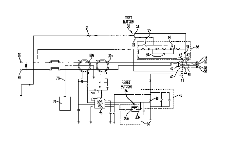
such as a solenoid or a relay, activates a latched circuit breaker mechanism
within the GFCI
device to enter a tripped state, thereby opening one or both sides of the AC
line, i.e., hot
and/or neutral, removing power to the load.
[0004] GFCI devices may be connected, for example, to fuse boxes or
circuit panels,
but more commonly, conventional GFCI devices are incorporated into electrical
receptacles
and installed at various locations within a building. Similar to regular
electrical receptacle
outlets these conventional GFCI devices have a set of conductive receptacle
terminals that are
accessible through slots in the face of the GFCI device. In many GFCI devices
these face
terminals are connected directly to the load terminals which are electrically
connected to the
line terminals when the latching mechanism is in a closed, or reset,
condition. When the
device is properly wired the AC power source is connected to the line
terminals of the GFCI
device and downstream load devices, such as additional GFCI devices or
regular, non-GFCI,
receptacles, are electrically connected to the load terminals.
[0005] If the GFCI device is "reverse wired," also referred to as
"miswired," where
the AC power source is connected to the load terminals instead of the line
terminals, a
- 2 -
CA 3077948 2020-04-20
potentially dangerous situation arises. That is, according to some
conventional GFCI devices,
when the load terminals are connected to an AC power source, and the
receptacle, or face,
terminals are electrically connected to the load terminals, the receptacle
terminals are always
powered, even if the circuit breaker, or latching mechanism, is not latched.
As a result, the
installer, and possibly the user, would be under the mistaken impression that
the GFCI is
operating correctly. The installer or user would be unaware that the GFCI is
not providing
fault protection, even when a fault condition is detected and the device
trips, as expected.
That is, if the device trips, for example in response to a real or test ground
fault, power is still
supplied to the face terminals and any device plugged into the face terminals.
This is because
AC power is directly connected to the load terminals which, in many older
devices, are
electrically connected to the face terminals.
[0006] To prevent such a potentially dangerous situation, Underwriters
Laboratories
(UL) Standard 943 requires that GFCI devices have a means to detect such
miswiring
conditions, and prevent power from being supplied to the face terminals in
such instances.
Thus, in accordance with UL standards, any attempt to reset a miswired GFCI
device should
prevent power from being provided to the face terminals. A solution employed
by some
manufacturers is to provide the GFCI to the installer in a tripped condition
where the latch
mechanism is in an open, unlatched, state such that no power is provided to
the face
terminals. The latch mechanism is then permitted to enter a closed, reset,
state only if the
device is properly wired. These types of GFCI devices typically utilize a
mechanical locking
mechanism that prevents the device from being reset until a properly wired
condition is
detected, at which point the locking feature is disabled. The locking feature
of these GFCI
devices is typically permanently disabled after the device is properly
installed. Thus,
according to these devices miswiring protection is only provided at the time
of initial
installation. This solution is particularly undesirable because the GFCI
device no longer
provides miswiring protection when the GFCI device is removed and/or re-
installed later.
[0007] Another undesirable characteristic of such devices is the
propensity for the
mechanical locking feature to malfunction due to something happening to the
device prior to
the first installation. Known causes of such malfunction include the device
being subjected
to strong vibrations or shock during shipping, for example, resulting from the
device being
dropped, or otherwise exposing the GFCI device to an impact. In this case, the
face terminals
will provide unprotected power unbeknownst to the user if the GFCI device is
miswired.
[0008] Further, it is known that even though manufacturers typically
advise
customers and the public to test their GFCI devices periodically by pressing
the "TEST"
- 3 -
CA 3077948 2020-04-20
button on the device, causing an intentional imbalance in the hot and neutral
currents in the
device, the devices are rarely tested as advised. Accordingly, some
manufacturers have
provided so-called "self-test" mechanisms within their GFCI devices for
automatically testing
the device without requiring human intervention. Conventional self-test GFCI
devices,
however, fail to test the device in a robust fashion where many of the device
components are
tested and false failures are ignored.
[0009] Thus, it is desirable to provide a GFCI device that includes
shock and/or drop
proof miswiring protection, which is re-installable after the device has been
removed or
power has been cut-off from the device and which optionally provides a robust
self-testing
feature for automatically testing the functionality of the device without
human intervention.
SUMMARY OF THE INVENTION
[0010] Exemplary embodiments of the present invention address at least
the above
problems and/or disadvantages and provide at least the advantages described
below.
Accordingly, an aspect of exemplary embodiments of the present invention is to
provide a
ground fault circuit interrupting (GFCI) device having a reset device
including a reset button
and a cylindrical reset pin, the reset pin having a flange portion and being
movable in a first
direction along its cylindrical axis, a latch block with an opening
therethrough, wherein the
reset pin passes freely through the opening in the latch block and the latch
block is movable
in the first direction. A latch plate is further provided in the GFCI device
that has a flat
portion with an aperture therethrough and an end portion substantially
perpendicular to the
flat portion, the latch plate being movable in a second direction transverse
to the first
direction. The exemplary GFCI device further includes a reset circuit with a
pair of electrical
contacts and a rigid electrically conductive member fixed to a first surface
of the latch block,
the rigid electrically conductive member contacting the pair of electrical
contacts and
completing the reset circuit to initiate a reset function when the reset
button is pressed.
[0011] A further embodiment of the invention includes a circuit
interrupting device
comprising a pair of line conducting members including at least a hot line
conducting
member and a neutral line conducting member, a pair of load conducting members
including
at least a hot load conducting member and a neutral load conducting member, a
pair of face
conducting members including at least a face conducting member and a neutral
face
conducting member, and a detection circuit configured to generate a detection
signal upon
detecting a current imbalance in at least one of the pairs of line, load and
face conducting
- 4 -
CA 3077948 2020-04-20
members. A circuit interrupting device in accordance with this exemplary
embodiment
further includes a latch assembly engaged with one or more of the line, load
and face
conducting members and for electrically connecting the line, load and face
conducting
members to place the circuit interrupting device in a reset state and
electrically isolate the
line, load and face conducting members to place said circuit interrupting
device in a tripped
state. An activation circuit is also provided in accordance with this
embodiment, the
activation circuit is electrically connected to the detection circuit and the
latch assembly and
configured to activate the latch assembly upon receiving the detection signal
from the
detection circuit. Also, a reset assembly is provided including a reset
circuit and a reset
mechanism, the reset circuit having a first electrical contact electrically
connected to the
detection circuit and a second electrical contact connected to the activation
circuit, wherein
the activation circuit is activated when the first and second electrical
contacts of the reset
circuit are electrically connected.
[0012] A
further embodiment of the invention includes a method of operation for a
GFCI device. The method includes connecting AC power to line terminals of the
GFCI
device, pressing a reset button of the GFCI device in a first direction, the
reset button being
attached to a reset pin, pushing a latch plate in the first direction with a
flange portion of the
reset pin, and pushing a latch block in the first direction with the latch
plate, the latch block
having a rigid conducting member attached to a bottom surface of the latch
block. According
to this method the following additional steps are also conducted, electrically
connecting two
auxiliary contacts of a reset circuit with the rigid conducting member,
activating an actuator
when the auxiliary contacts are electrically connected, moving the latch plate
with the
actuator in a direction transverse to the first direction when the actuator is
activated, aligning
a first aperture in the latch block with a second aperture in the latch plate,
moving the latch
plate with a first resilient member in a direction opposite the first
direction when the first and
second apertures are aligned, wherein the flange portion of the reset pin
passes through the
second aperture of the latch plate, deactivating the actuator, moving the
latch plate with a
second resilient member in a direction opposite the second direction when the
actuator is
deactivated, and pulling the latch block with the should portion of the reset
pin in the
direction opposite the first direction. If AC power is not properly connected
to the line
terminals, the actuation cannot be activated and, thus, the device will not be
placed into the
reset condition. That is, the latch block will never ultimately be pulled up
where the line,
load and face contacts will be electrically connected.
- 5 -
CA 3077948 2020-04-20
100131 A further embodiment of the invention includes a circuit
interrupting device
having a hot line terminal and a neutral line terminal for electrically
connecting to an AC
power source, a hot load terminal and a neutral load terminal for electrically
connecting to an
electrical load, a first electrical conductor disposed between the hot line
terminal and the hot
load terminal, a second electrical conductor disposed between the neutral line
terminal and
the neutral load terminal, a fault detecting circuit operable to detect at
least one type of fault
and generate a fault detection signal when the fault is detected, an
interrupter electrically
connected to the first and second conductors and the hot and neutral load
terminals and being
operable to electrically disconnect one or more of the hot line terminal from
the hot load
terminal and the neutral line terminal from the neutral load terminal when
actuated, a first
switching device electrically coupled to the fault detecting circuit and
closing when the fault
detection signal is received from the fault detecting circuit, a second
switching device
electrically coupled to an output of the first switching device and closing as
a result of the
first switching device closing, and a third switching device electrically
coupled to an output
of the first switching device and closing as a result of the first switching
device closing,
wherein the interrupter is actuated when at least one of the second and third
switching
devices is closed.
100141 A still further embodiment of the invention includes a circuit
interrupting
device with a housing having a front cover and a rear cover, a hot line
terminal and a neutral
line terminal for electrically connecting to an AC power source, a hot load
terminal and a
neutral load terminal for electrically connecting to an electrical load, a
first electrical
conductor disposed between the hot line terminal and the hot load terminal, a
second
electrical conductor disposed between the neutral line terminal and the
neutral load terminal,
a detecting circuit operable to detect a magnetic flux and generate a
detection signal when the
flux is detected, an interrupter electrically connected to the first and
second conductors and
the hot and neutral load terminals and operable to electrically disconnect one
or more of the
hot load terminal from the hot line terminal and the neutral load terminal
from the neutral line
terminal when actuated, and an auto-monitoring circuit electrically coupled to
the detecting
circuit and operable to generate a test magnetic flux to be detected by the
detecting circuit,
wherein the rear cover of the housing includes a recessed receptacle in which
the hot line
terminal and the neutral line terminal are disposed, the recessed receptacle
being configured
to receive a power plug connected to AC power.
- 6 -
CA 3077948 2020-04-20
[0015] Aspects, advantages and salient features of the invention will
become apparent
to those skilled in the art from the following detailed description, which,
taken in conjunction
with annexed drawings, discloses exemplary embodiments of the invention.
BRIEF DESCRIPTION OF THE DRAWINGS
[0016] The above and other exemplary features and advantages of
certain exemplary
embodiments of the present invention will become more apparent from the
following
description of certain exemplary embodiments thereof when taken in conjunction
with the
accompanying drawings in which:
[0017] FIG. 1A is a top perspective view of a ground fault circuit
interrupting (GFCI)
device in accordance with an exemplary embodiment of the present invention;
[0018] FIG. 1B is a top perspective view of a ground fault circuit
interrupting (GFCI)
device in accordance with a second exemplary embodiment of the present
invention;
[0019] FIG. 2A is a bottom perspective view of the ground fault
circuit interrupting
device shown in FIG. 1A;
[0020] FIG. 2B is a bottom perspective view of the ground fault
circuit interrupting
device shown in FIG. 2A;
[0021] FIG. 3A is a schematic diagram of an exemplary electric circuit
of the ground
fault circuit interrupting device of FIG. 1A;
[0022] FIG. 3B is a schematic diagram of an exemplary electric circuit
of the ground
fault circuit interrupting device of FIG. 2A;
[0023] FIG. 4 is a cross sectional view illustrating the various
mechanical
components within the ground fault circuit interrupting device of FIG. 1 in
accordance with
an exemplary embodiment of the present invention;
[0024] FIG. 5A is an enlarged cross sectional side view of a portion
of the latch
assembly and spring mechanism within the solenoid housing of the ground fault
circuit
interrupting device of FIG. 1 in accordance with an embodiment of the present
invention;
[0025] FIG. 5B is an enlarged cross sectional front view of a portion
of the latch
assembly and spring mechanism within the solenoid housing of the ground fault
circuit
interrupting device of FIG. 5A in accordance with an embodiment of the present
invention;
[0026] FIG. 5C is a perspective view of an exemplary embodiment of a
latch block
assembly in accordance with the present invention;
- 7 -
CA 3077948 2020-04-20
[0027] FIG. 6A is an enlarged cross sectional view of a portion of the
latch assembly
and reset mechanism in the tripped condition, within the solenoid housing of
the ground fault
circuit interrupting device of FIG. 1 in accordance with an embodiment of the
present
invention;
[0028] FIG. 6B is an enlarged cross sectional view of a portion of the
latch assembly
and reset mechanism within the solenoid housing of the ground fault circuit
interrupting
device of FIG. 1 as the reset button is initially being pressed, in accordance
with an
embodiment of the present invention;
[0029] FIG. 7A is an enlarged cross sectional view of a portion of the
latch assembly
and reset mechanism within the solenoid housing of the ground fault circuit
interrupting
device of FIG. 1 when the reset button is fully pressed and the switch on the
PCB is closed, in
accordance with an embodiment of the present invention;
[0030] FIG. 7B is an enlarged cross sectional view of a portion of the
latch assembly
and reset mechanism within the solenoid housing of the ground fault circuit
interrupting
device of FIG. 1 after the solenoid has fired;
[0031] FIG. 8 is a cross-sectional view of an alternative construction
for the reset pin
assembly in accordance with a further embodiment of the present invention;
[0032] FIG. 9A is an enlarged cross sectional view of a portion of the
latch assembly
and reset mechanism within the solenoid housing of the ground fault circuit
interrupting
device of FIG. 1 after the latch plate clears the reset pin and the latch
assembly is permitted to
rise, opening the switch on the PCB;
[0033] FIG. 9B is an enlarged cross sectional view of a portion of the
latch assembly
and reset mechanism within the solenoid housing of the ground fault circuit
interrupting
device of FIG. 1 after the latch plate is permitted to retract;
[0034] FIG. 10 is an enlarged cross sectional view of a portion of the
latch assembly
and reset mechanism within the solenoid housing of the ground fault circuit
interrupting
device of FIG. 1 after the reset pin is released and pulls the latch assembly
up under the bias
of the reset spring;
[0035] FIG. 11A is a perspective view showing the interrupter contacts
in the open
position and other internal components of the ground fault circuit
interrupting device of FIG.
1 in accordance with an embodiment of the present invention;
[0036] FIG. 11B is a perspective view showing the interrupter contacts
in the closed
position and other internal components of the ground fault circuit
interrupting device of FIG.
1 in accordance with an embodiment of the present invention;
- 8 -
CA 3077948 2020-04-20
[0037] FIG. 11C is a perspective view showing the face terminal
manifold holding
the face terminals and the end-of-life indicator in accordance with an
embodiment of the
present invention;
[0038] FIG. 12 is an enlarged cross sectional view of a portion of the
latch assembly
and reset mechanism within the solenoid housing of the ground fault circuit
interrupting
device of FIG. 1 after the test button is pressed and the solenoid fires,
pushing the plunger
into the latch plate;
[0039] FIG. 13 is an enlarged cross sectional view of a portion of the
latch assembly
and reset mechanism within the solenoid housing of the ground fault circuit
interrupting
device of FIG. 1 after the solenoid has fired and the latch plate has cleared
the reset pin
allowing the latch assembly to drop and open the interrupter contacts as shown
in FIG. 11B;
[0040] FIGS. 14A-14C are schematic drawings illustrating an
alternative
embodiment of the present invention.
[0041] Throughout the drawings, like reference numerals should be
understood to
refer to like elements, features and structures.
DETAILED DESCRIPTION OF EXEMPLARY EMBODIMENTS
[0042] The matters exemplified in this description are provided to
assist in a
comprehensive understanding of exemplary embodiments of the present invention
disclosed
with reference to the accompanying figures. Those of ordinary skill in the art
will recognize
that various changes and modifications of the exemplary embodiments described
herein can
be made without departing from the scope and spirit of the claimed invention.
Also,
descriptions of well-known functions and constructions are omitted for clarity
and
conciseness.
[0043] FIG. 1A is a perspective view of an exemplary ground fault
circuit
interrupting (GFCI) receptacle device 10 in accordance with an embodiment of
the present
invention. The GFCI device 10 includes a housing 12 having a cover portion 14
and a rear
portion 16. GFCI 10 also includes an inner housing (see, for example, FIG. 4)
visible when
the cover portion 14 is removed from the rear portion 16. Cover portion 14 and
rear portion
16 are removably secured to each other via fastening means such as clips,
screws, brackets,
tabs and the like. Because the embodiment shown in FIG. 1A is a duplex
receptacle device,
cover portion 14 includes two pair of plugin slots 18 and 20 (also referred to
as face
receptacles) and two grounding slots 22. It will be appreciated by those
skilled in the art that
- 9 -
CA 3077948 2020-04-20
plugin slots 18 and 20 and grounding slots 22 can accommodate polarized, non-
polarized,
grounded or non-grounded blades of a male plug. The male plug can be a two-
wire or three-
wire plug without departing from the scope of the present invention. GFCI
receptacle 10
further includes ground strap 24 having mounting holes 26 for mounting GFCI
receptacle 10
to a junction box (not shown). Grounding screw 28 for connecting to a ground
conductor is
disposed at the rear wall of housing 12.
[0044] Rear portion 16 includes four terminal screws, 37-40, of which
only screws 38
and 40 are shown in FIG. 1A. When the GFCI device is properly installed, load
side terminal
screw 38 is connected to a load side neutral conductor and an opposing load
side terminal
screw 37 (See FIG. 2A) is connected to a load side hot conductor. Line side
terminal screw
40 is connected to the neutral conductor of a power supply, and an opposing
line terminal
screw 39 (See FIG. 2A) is connected to the hot conductor of the power supply.
It will be
appreciated by those skilled in the art that GFCI receptacle 10 can also
include apertures
proximate the line and load terminal screws 37-40 to receive the bare end of
the conducting
wires rather than connecting the bare end of the wires to the line and load
terminal screws.
[0045] Still referring to FIG. 1A, test button 30 extends through
opening 32 in cover
portion 14 of housing 12. Depressing the test button activates a test
operation that tests the
circuit interrupting components disposed in GFCI receptacle 10. The circuit
interrupting
components, to be described in detail below, are used to break electrical
continuity in one or
more conductive paths between the line and load sides of the GFCI receptacle
10, and the
user-accessible face terminals, by transitioning a latching mechanism to enter
an unlatched,
or "tripped," state. Reset button 34 extends through opening 36 in cover
portion 14 of
housing 12. Depressing reset button 34 activates a reset operation to place
the latching
mechanism in a latched, or "reset," state that reestablishes electrical
continuity in the open
conductive paths, that is, it reestablishes electrical continuity between the
line, load and face
contacts.
[0046] FIG. 113 depicts a further exemplary embodiment of a GFCI
receptacle device
in accordance with the invention. In particular, GFCI 100 is similar to GFCI
10 in FIG. 1A
in some respects, but GFCI device 100 has several important differences.
Housing 112
includes cover portion 114 and rear portion 116. Similar to GFCI 10, cover
portion 114
includes two pair of plugin slots 18 and 20 and two grounding slots 22. GFCI
device 100
further includes ground strap 24 having mounting holes 26 for mounting the
GFCI receptacle
100 to a junction box (not shown). GFCI 100 does not include terminal screws
37-40, as
shown in FIG. 1A, because GFCI 100 is connected to AC power via a plug-in
terminal on the
- 10 -
CA 3077948 2020-04-20
back of rear cover 116, as shown in FIG. 2B. Also, cover portion 114 of GFCI
100 includes
a visible indicator 132, such as an LED, to indicate the status of one or more
conditions of the
device, which are described in more detail below.
[0047] Referring to FIG. 2B, rear cover 116 includes an input power
receptacle 120.
Input power receptacle 120 connects with a "keyed," i.e., having a
corresponding shape to
input receptacle 120, input power connector (not shown) which provides AC
power to the
device. Input receptacle 120 includes male ground blade 122, male neutral
blade 124 and
male hot blade 126. Blade 126 connects to the hot, or phase, side of the input
power
connector, blade 124 connects to the neutral side of the input connector and
ground blade 122
connects to the ground connection of the input connector. In comparison to
GFCI device 10
shown in FIG. 1A, GFCI 100, thus, provides a convenient mechanism by which AC
power is
applied to the device, i.e., by way of the input connector. Further, because
of the shape of
input receptacle 120, for example, as provided by curved portion 128, the
input connector can
only be inserted into receptacle 120 if it is correctly oriented. That is, a
curved portion on the
input connector must be similarly shaped and aligned with curved portion 128
on receptacle
120 before the connector can be inserted into the receptacle. Accordingly, it
is virtually
impossible to miswire the device. Specifically, because the input connector
can only be
inserted into the input receptacle one way, the hot conductor in the input
connector cannot be
connected to the neutral or ground conductors of the input receptacle, and
vice versa.
[0048] FIG. 3A is an electrical schematic diagram illustrating circuit
interrupting
components of an exemplary GFCI device in accordance with the invention. The
circuit
depicted in FIG. 3A is consistent with and can be implemented as part of
either GFCI 10 or
GFCI 100 shown respectively in FIGS. 1A and 1B. For ease of description here,
however,
the circuit of FIG. 3A is described in connection with GFCI 10, as shown in
FIG. 1A. In
accordance with this embodiment, the circuit interrupting components of GFCI
device 10
include test button 30, reset button 34, which is provided as part of reset
circuit 35, latch
assembly 50, firing circuit 48, sensing transformer 90A, ground transformer
90B, and a GFCI
chip 70. GFCI chip 70 according to this embodiment is a commercially available
GFCI
device, such as, an RV4141 or RV4145 by Fairchildm.
[0049] Latch assembly 50 includes contact assembly 47 and solenoid 51.
Further,
contact assembly 47, an exemplary embodiment of which is shown more clearly in
FIGS.
11A and 11B, includes a plurality of contact pairs, 41-42, 43-44, 45-46,
electrically
connected to line terminals, screws, (39, 40), load terminals, screws, (37,
38) and face
terminals (18, 20), respectively. When latch assembly 50 is in the latched
state, the hot line,
- 11 -
CA 3077948 2020-04-20
hot load and hot face contacts (41, 43, 45, respectively) are electrically
connected together,
and the neutral line, neutral load and neutral face contacts (42, 44, 46,
respectively) are
electrically connected together. Thus, when the device is latched in the reset
state and AC
power is applied to the device, power is also provided to the load and face
terminals.
100501 Firing circuit 48 includes a silicon controlled rectifier (SCR)
49 that functions
as a switch to control current flow through solenoid 51, as described further
below. The
electrical components depicted in FIG. 3A and described above, are preferably
interconnected on a printed circuit board (PCB).
[0051] The components of GFCI devices 10 and 100, as illustrated in
FIGS. 3A and
3B, are structured and arranged to prevent miswiring of the GFCI device during
installation.
For example, prior to installation of GFCI device 10, latch assembly 50 is
provided in an
unlatched state such that the line, load and face contacts of contact assembly
47 are not
electrically connected. In this unlatched state, the power supply is cut-off
from the face
terminals, 18, 20, as well as from any other loads connected downstream from
the GFCI via
load terminals 37, 38. Power is provided to face terminals, 18,20, only if the
power supply is
properly connected to the line side terminals 39, 40 and the device is in the
latched state. To
initiate a latched, "reset", state of the latch assembly 50, a user presses
the reset button 34 to
electrically connect secondary contacts 33a and 33b provided on the PCB and
close reset
circuit 35.
[0052] When reset circuit 35 is closed, the gate of SCR 49 is
energized by GFCI IC
device 70 and if GFCI 10 is correctly wired to the live power source current
flows through
SCR 49. That is, GFCI IC device 70 is only powered and able to gate SCR 49
when AC
power is connected to the line side terminals, 39, 40. When SCR 49 is ON,
i.e., its gate is
activated, it passes current drawn from the hot line terminal 39 through
solenoid 51 to
electrical ground. As described in greater detail below with respect to FIGS.
6-10, a plunger
provided within the coil of solenoid 51 is forced, due to a magnetic field
generated around the
coil, to move in a predetermined direction moving a latch plate 54 (FIG.4).
Latch plate 54
moves to a position such that upon release of the reset button, the latch
assembly 50 enters
the latched state to connect the contacts of the contact assembly, as shown in
FIG. 10C.
[0053] If GFCI device 10 is miswired, and AC power is connected to
load terminals
37, 38, upon the user pressing reset button 34, SCR 49 will not turn ON
because GFCI IC
device 70 will be unable to provide a voltage on the gate of SCR 49.
Accordingly, no current
will be drawn through solenoid 51 to enable the latch assembly 50 to enter the
latched state
and the device will remain in the tripped state.
- 12 -
CA 3077948 2020-04-20
[0054] The exemplary circuit of FIG. 3A also includes optional
microprocessor 75
with electrical conductor 76 connected between microprocessor 75 and ground.
Conductor
76 traverses through transformer 90A and conducts current through the
transformer when
microprocessor 75 outputs a test signal on conductor 76. Further information
regarding the
operation and configuration of microprocessor 75 is provided in, for example,
U.S. Patent
7,443,309, which may be referred to for further details.
[0055] FIG. 3B is an electrical schematic of a circuit in accordance
with a further
embodiment of the invention. Specifically, FIG. 3B depicts a circuit for a
self-testing
embodiment in accordance with the present invention. It is noted that the
circuit shown in
FIG. 3B is consistent with and can be implemented in either of GFCI device 10
or GFCI 100.
Also, the electro-mechanical aspects of the operation of a GFCI device
utilizing the circuit of
FIG. 3B are consistent with the description of the operations provided below
with respect to
FIGS. 4-7 and 9-13. For simplicity and ease of discussion, however, the
operational
description with respect to these figures is provided below in reference to
the GFCI device 10
shown in FIGS. 1A and 2A and the circuit shown in FIG. 3A. Specific additional
details
related to the circuit of FIG. 3B are provided subsequently.
[0056] FIG. 4 depicts a cross-section of internal housing 13 according
to exemplary
GFCI device 10. In FIG. 4, cover portion 14 (FIG. 1A) of housing 12 has been
removed to
expose internal housing 13. Internal housing 13 includes latch assembly 50
which includes
"T"-shaped latch plate 54. Latch plate 54 slidably extends through the latch
assembly 50, as
shown, and is secured to latch assembly 50 such that they move together during
both the
latching and tripping sequences, in the directions shown by the arrow "A".
Reset pin 56 is
provided through a central opening in latch assembly 50 with reset button 34
provided at the
end of the reset pin extending out of the central opening 36 in the GFCI cover
14 (FIG.1A).
Reset pin 56 has an annular reset flange 61 extending radially outwardly from
reset pin 56
and having first upwardly facing surface 61a and second downwardly facing
surface 6 lb near
the end of the reset pin 56 opposite the reset button 34 at the upper end. As
discussed further
below, first and second surfaces 61a, 61b engage with lower and upper
surfaces, respectively,
of the latch plate 54 to initiate a reset operation and to position the latch
plate 54 in the
latched state. Reset pin 56 is surrounded by a helical spring element 55
provided between the
reset button 34 and a support surface in the latch assembly 50. In the tripped
position, reset
button 34 is urged upward in FIG. 4 by spring element 55.
[0057] A conductive shorting bar 58a, more easily seen in FIG. 6A, is
provided at a
lower end of the latch assembly 50 on a surface facing the printed circuit
board (PCB) 65.
- 13 -
CA 3077948 2020-04-20
Secondary switch contacts 33a and 33b are provided on PCB 65 at a position
facing shorting
bar 58a. Shorting bar 58a is preferably a rigid member composed of a
conducting material,
such as metal, and has a length at least equal to the distance between the
secondary contacts
33a and 33b provided as part of the reset circuit 35 (FIG. 3A). Shorting bar
58a is electrically
isolated from secondary switch contacts 33a and 33b at all times, except
during the user
initiated reset operation. Specifically, latch assembly 50 is suspended above
PCB 65 to
prevent shorting bar 58a from contacting the secondary switch contacts and,
thus, shorting
the reset circuit except when a user presses reset button 34 to initiate the
reset operation.
100581 In a further embodiment, shorting bar 58a is attached to the
latch assembly 50
with one or more intervening spring elements to provide additional travel for
the latch
assembly. For example, in accordance with this further embodiment one or more
springs,
such as coil springs, leaf springs, etc., are placed between the bottom of
latch assembly 50
and shorting bar 58a. When reset button 34 is pressed, spring element 55
begins to compress
as shorting bar 58a moves downward toward secondary switch contacts 33a, 33b.
When
shorting bar 58a makes contact with switch contacts 33a, 33b, the spring
element(s) between
the shorting bar and the bottom of the latch assembly begin to compress as
reset button 34
continues to be pressed and reset spring 55 continues to compress.
100591 Solenoid 51 is provided within solenoid housing 60. Plunger 52,
spring
element 62 and spacer 64 are all provided within solenoid 51 and are coaxially
therewith. As
shown, plunger 52 and spring element 62 abut against an outer surface of side
wall 66 of the
"T"-shaped latch plate 54. Latch plate 54 is held in its initial position by
the force of helical
spring element 67 provided between an inner surface of side wall 66 and a
lower end of the
latch assembly 50. In the absence of a magnetic field around solenoid 51, the
force of spring
element 67 overcomes the force of spring element 62 provided within solenoid
51, side wall
66 of latch plate 54 remains pressed against flange 69 of the solenoid
housing.
100601 FIGS. 5A, 5B are enlarged side and front cross-sectional views,
respectively,
of an exemplary embodiment of latch assembly 50. As shown, latch assembly 50
is
suspended above the PCB 65 by spring elements 57a and 57b provided between the
two pairs
of retaining pegs 59a and 59b. According to this embodiment, retaining pegs
59b are
provided as part of the solenoid housing 60, while retaining pegs 59a are
provided as part of
the latch assembly 50, as shown. Retaining pegs 59a are provided on the
outwardly
protruding surfaces or arms 50b integral with and extending laterally away
from the latch
assembly 50. Retaining pegs 59a and 59b not only retain the spring elements
57a and 57b but
they also provide reactive surfaces for the spring elements 57a and 57b, to
keep the latch
- 14 -
CA 3077948 2020-04-20
assembly 50 floating or suspended above PCB 65. The force provided by spring
elements
57a and 57b is sufficient to maintain the latch assembly 50 in the floating
position in the
absence of an external force, for example when a user presses the reset button
to begin the
reset operation.
100611 As described in greater detail below with respect to FIGS. 11A,
11B, when
GFCI device 10 enters the latched state, laterally extending arms 50b of latch
assembly 50
urge cantilevered load contact arms 80 and 81 into engagement with
cantilevered line contact
arms 82 and 83, respectively, to supply power to the face and load terminals.
Because load
contact arms 80 and 81 electrically connect with line contact arms 82 and 83,
respectively, in
the latched state, load contact arms 80 and 81 are preferably formed as
resilient cantilevers
that are effectively biased toward PCB 65, away from line contact arms 82 and
83. To
prevent cantilevered load arms 80 and 81 from undesirably forcing the latch
assembly arms
50b, and, thus, the latch assembly 50, against the bias of the spring elements
57a and 57b
toward the PCB 65 in the unlatched state, solenoid housing 60 also preferably
includes at
least one fixed or built-in stop 68a providing a stop surface against which
the cantilevered
load arms 80 and 81 rest, thus, stopping further downward movement. Fixed stop
68a
prevents the cantilevered arms from providing a force on the latch assembly
arms 50b, by
blocking movement of the cantilevered arms in the biased direction when the
cantilevered
arms contact the fixed stop. Fixed stop 68a is provided as an additional means
to ensure that
the latch assembly 50 remains suspended above PCB 65 in the absence of an
applied force by
a user to initiate the reset mechanism. A similar fixed stop 68b is also
preferably provided on
the opposite side of solenoid housing 60 to provide a similar stop surface for
the cantilevered
line arms 82 and 83. Fixed stop 68b prevents a dangerous situation from
occurring where the
cantilevered line arms 82 and 83 may be urged by the effective bias of the
cantilever to
contact the load arms 80 and 81, while the GFCI is in an unlatched state.
[0062] FIGS. 6-10 are perspective views illustrating the sequence of
operation of the
latching mechanism of the exemplary GFCI device 10 as it enters the latched,
"reset," state.
As illustrated in FIG. 6A, according to this exemplary embodiment the GFCI
device is in the
unlatched, or "tripped," condition. This is the condition the device is in
when it is provided
from the manufacturer. As shown, latch assembly 50 in the initial unlatched
state is
suspended above the printed circuit board (PCB) 65, such that there is no
physical contact
between shorting bar 58a and secondary PCB contacts 33a and 33b. In the
unlatched state,
latch plate 54 is positioned below the contact flange of the reset pin formed
by first and
second contact surfaces 61a, 6 lb of reset flange 61. In this unlatched
position, as described
- 15 -
CA 3077948 2020-04-20
further below with respect to FIG. 11A, line side contacts 41 and 42 are not
able to contact
load side contacts 43 and 44, respectively, thus preventing power from being
supplied to any
load side devices or face terminals 18, 20 (FIG. 1) of the GFCI device. Thus,
in the initial
state, prior to the reset operation, there is no power supplied to face
terminals 18, 20
regardless of whether or not the GFCI device is correctly wired to a power
source.
100631 After the GFCI device is correctly wired to a power source by
connecting the
hot and neutral conductors of the power source to the line terminals 39 and
40, respectively, a
reset operation is performed before power will be supplied to the face
terminals 18, 20 and
load terminals 37, 38. To initiate a reset, i.e., to place the latch assembly
in a latched state, a
user presses the reset button 34 protruding from GFCI cover 14 against the
force of the spring
element 55 surrounding reset pin 56. Reset pin 56 moves in the same direction
as reset
button 34 into the GFCI housing toward latch plate 54. As shown in FIG. 6B,
bottom surface
61b of reset flange 61 contacts latch plate 54. Prior to contacting latch
plate 54, reset pin 56,
including reset flange 61, moves axially through a hole in the body of latch
assembly 50
without effecting movement of the latch assembly. Due to the engagement with
the latch
plate 54, which is movable in the same direction with the latch assembly 50,
and upon
continued pressing of reset button 34, latch assembly 50 moves against the
force of spring
elements 57a, 57b, shown in FIG. 5B, together with the reset pin 56.
[0064] As shown in FIGS. 7A, 7B, downward movement of latch assembly
50 and
latch plate 54 continues until shorting bar 58a comes into contact with
secondary contacts
33a, 33b provided on PCB 65, thus closing the reset switch (34 in FIG. 3A, 300
in FIG. 3B).
Secondary contacts 33a, 33b, provided on PCB 65, form a first part of the
reset switch.
When shorting bar 58a contacts secondary contacts 33a, 33b, the reset switch
is closed, thus,
providing a conductive path between the gate of SCR 49 (FIG. 3A) and the
voltage output pin
of the microcontroller 70. If GFCI device 10 is wired correctly, an electric
current will be
supplied to the gate terminal of SCR 49 through this closed conductive path.
The supplied
current transitions SCR 49 into a conducting/operating state and current is
drawn through
solenoid 51 from the correctly wired hot line terminal 39. The current now
flowing generates
a magnetic field at solenoid 51 that forces, i.e., fires, plunger 52 in a
direction that slightly
compresses spring 62 against the side wall 66 and pushes spacer 64 against
sidewall 66 of
latch plate 54.
[0065] Referring to FIG. 7B, the magnetic force applied to plunger 52
by the coil of
solenoid 51 is sufficient to overcome the opposing force asserted by spring
element 67
positioned between the side wall 66 of latch plate 54 and a spring retaining
peg on latch
- 16 -
CA 3077948 2020-04-20
assembly 50. As a result, latch plate 54 is moved, to the right in FIG. 7B, by
plunger 52 and
hollow spacer 64 through a slot in latch assembly 50, as shown. In this
position, an aperture
71 in latch plate 54 aligns with reset flange 61 on reset pin 56 such that the
second, or
bottom, surface 61b of the reset flange no longer contacts the latch plate. In
an exemplary
embodiment, spring elements 57a, 57b (FIG. 5A, 5B) provide a resilient buffer
against
excessive force asserted on the reset pin by a user initiating the reset
operation. Specifically,
as the user presses the reset button to initiate the condition shown in FIG.
7B, springs 57a,
57b compress. Springs 57a, 57b reduce an effective force on the surface of the
latch plate 54
when the shorting bar closes the reset switch to initiate the firing of the
plunger 52. Because
the reset switch is closed. i.e., by the shorting bar 58a, before latch
assembly 50 "bottoms
out" on the PCB board, springs 57a, 57b absorb some of the downward force
applied by reset
flange 61 on latch plate 54. This ensures that latch plate 54 moves to the
desired position
upon firing of plunger 52, as described above.
[0066] In a further exemplary embodiment, shown for example in FIG. 8,
cylindrical
reset pin 156 with internal spring element 155 is provided instead of, or in
addition to, springs
57a, 57b shown in FIG. 7B. In this embodiment, shorting bar 58a may be
attached directly to
the lower end of the latch assembly, as opposed to having one or more
intervening springs,
such as springs 160a, 160b included in the embodiment of FIG. 5C. Reset pin
156 comprises
at least two portions 157, 158. Upper portion 157 of reset pin 156 has a
hollow cavity, 159
with a retaining peg at the top end thereof for retaining one end of spring
155. Lower portion
158 of the reset pin 156 includes reset flange 161 with upper and lower
surfaces 161a, 16 lb,
respectively, and extends outside of hollow cavity 159. Lower portion 158 is
attached to the
hollow upper portion 157 with a spring element 155. Spring element 155 is
preferably
provided with a biasing strength at least slightly greater than the upward
force of the latch
assembly 50. Spring element 155 provides a buffer to reduce an effective force
of the reset
pin 156 on latch plate 54. Thus, latch plate 54 is not prevented from moving
to the desired
position upon firing of plunger 52, as described above.
[0067] Regarding the embodiment illustrated in FIGS. 6A, 6B and 7A,
7B, continued
pressing of reset button 34 moves reset pin 56 down through a cavity in latch
assembly 50, as
shown in FIG. 9A. Because the second, lower, surface 61b of reset flange 61 is
no longer in
contact with latch plate 54, the reset flange moves through aperture 71 in
latch plate 54 to the
position shown in FIG. 9A. Also, because latch assembly 50 is no longer forced
by the
pressing of the reset button against the bias of the spring elements 57a, 57b,
as shown in
FIGS. 5A, 5B, spring elements 57a, 57b urge the latch assembly up and away
from being in
- 17 -
CA 3077948 2020-04-20
contact with PCB 65. Further, because latch assembly 50 is urged away from PCB
65,
shorting bar 58a on the latch assembly is also urged away from the PCB and no
longer
contacts the secondary contacts 33a, 33b on the PCB, thus, opening reset
circuit 35 between
the gate of SCR 49 and the GFCI IC device 70 (see e.g., FIG. 3A).
[0068] Because the gate of SCR 49 is no longer activated when shorting
bar 58a
disconnects from the secondary contacts 33a, 33b, SCR 49 transitions back to a
non-
conducting/non-operating state. Consequently, current is no longer drawn
through solenoid
51 and the magnetic field ceases. Without the magnetic field to push plunger
52 and spacer
64 against latch plate 54, spring element 67 contacting side wall 66 of the
latch plate 54,
pushes spacer 64 and plunger 52 to the left in FIG. 9B and urges the latch
plate to its initial
position. Latch plate 54 slides sideways in the slot within latch assembly 50
such that
aperture 71 in the latch plate is no longer aligned with reset flange 61. When
reset button 34
is released by the user, the reset button and reset pin 56 are urged by reset
return spring
element 55 in the direction away from PCB 65, e.g., upward in FIGS. 9A, 9B.
[0069] Referring to FIG. 10, when the user releases the reset button
(see, e.g., FIG. 4),
reset pin 56, which now engages the underside of the latch plate 54 with the
first, top, surface
61a of reset flange 61, pulls the latch plate 54 up in a direction away from
PCB 65. The
GFCI device 10 and latch assembly 50 are now said to be in the latched state
because
contacts 41, 43, 45 (FIG. 11C) are electrically connected and contacts 42, 44,
46 (FIG. 11C)
are electrically connected. Because latch plate 54 is movable in the same
direction as latch
assembly 50, the latch assembly also moves in the same direction due to the
force applied by
the spring element 55 surrounding reset pin 56. Specifically, as latch
assembly 50 is pulled in
the "up" direction, farther away from the PCB 65, laterally extending arms 50b
(FIG. 5B) of
the latch assembly pull contacts 43, 44 on the free end of cantilevered load
arms 80 and 81,
respectively, into direct contact with the line contacts 41, 42 provided on
the cantilevered line
arms 82 and 83, respectively. When latch assembly 50 is pulled up and the
device enters the
latched condition, cantilevered arms 80-83 and contacts 41- 44 are disposed as
illustrated in
FIG. 11B.
[0070] FIGS. 11A and 11B illustrate, among other things, an exemplary
embodiment
of the contact assembly 47 shown in FIG. 3A and described above. FIG. 11A
shows GFCI
device 10 in the unlatched state. As shown, in the unlatched state, line
contacts 41 and 42 do
not contact load contacts 43 and 44. Accordingly, no current flows between the
line
terminals, 39, 40 and the load terminals 37, 38. As discussed with respect to
FIG. 1A, if the
GFCI device is properly wired, line hot and line neutral conductors connected
to an AC
- 18 -
CA 3077948 2020-04-20
power supply are connected to line hot and neutral terminals 39 and 40,
respectively. Load
hot and load neutral conductors are similarly connected to load hot and
neutral terminals 37
and 38, respectively. Line terminals 39 and 40 are electrically connected to
the cantilevered
line arms 82 and 83, respectively. A plurality of electrically conducting
contacts, 41 and 42,
are provided at the free end of the cantilevered line arms 82, 83,
respectively. According to
the present embodiment, line contacts 41 and 42 are staked into holes in the
ends cantilevered
arms 82 and 83, respectively, and include surfaces that face load contacts 43
and also include
surfaces that face upward, towards face contacts 45, 46 (not shown) and 44.
Face contacts
45, 46 are provided on separate electrically conducting members located on a
separate
housing (not shown). Although not shown, face contacts 45, 46 are electrically
connected to
the face terminals 18, 20 provided on the top cover 14, and electrically
connect with contacts
41, 42, respectively, when the GFCI device 10 is in the latched state. Due to
the natural bias
of the resilient cantilevered line arms 82, 83, contacts 41, 42 are urged away
from connecting
to the face contacts 45, 46 when the GFCI device 10 is in the unlatched or,
tripped, state.
10071] As seen in FIG. 11A, load hot terminal 37 and load neutral
terminal 38 are
electrically connected to cantilevered load arms 80 and 81, respectively. Load
contacts 43
and 44 are provided at the free ends of the cantilevered load arms 80 and 81,
respectively,
facing the line contacts 41 and 42 on the resilient cantilevered line arms 82
and 83,
respectively. In the unlatched state, as shown in FIG. 11A, due to the natural
bias of the
cantilevered load arms 80 and 81, the load contacts are urged away from
contacting with line
contacts 41 and 42, respectively. As previously discussed with respect to FIG.
5A, fixed stop
68b provides a surface for preventing the line contacts 41 and 42 from
"dropping" onto the
load contacts 43 and 44, respectively. Contacts 41-46 are preferably composed
of, and/or
coated with, an electrically conducting material that prevents any undesired
arcing between
the contacts.
10072] According to the embodiment shown in FIG. 11B, when the GFCI
device
enters the latched state, as described above, the bias of reset return spring
element 55 forces
the reset button and reset pin upwards, thus pulling the latch plate and latch
block upwards as
well. Laterally extending arms 50b (see, e.g., FIG. 5B), on either side of
latch assembly 50,
urge the resilient cantilevered load arms 80, 81, along with load contacts 43
and 44, upwards
to make contact with line contacts 41 and 42, respectively. As the latch
assembly 50
continues to move upwards, the face contacts 45 and 46 are contacted by line
contacts 41, 42
which are thus, brought into electrical contact with face terminals 18 and 20.
AC power is
now provided to face terminals 18, 20 on the outer housing of the GFCI device
and to any
- 19 -
CA 3077948 2020-04-20
device connected downstream to the load terminals 37, 38. In the configuration
shown in
FIG. 11B, GFCI device 10 is now in the latched, or reset, state.
[0073] Because GFCI device 10 is initially provided in an unlatched
state and proper
wiring is required before it can enter the reset state, there is no need to
provide any locking
mechanism or lock-out mechanism that could potentially be defeated prior to
installation.
The GFCI device will only enter the reset state when the GFCI device is
properly wired
during installation such that AC power is provided at the line terminals.
Therefore, miswire
protection of GFCI device 10 cannot be defeated prior to installation and a
potentially
dangerous situation where the GFCI device is incorrectly wired unbeknownst to
the user but
power is applied to the face terminals can be prevented. Additionally, the
above exemplary
latching mechanism is capable of repeatedly detecting a miswire condition
without any
specific additional operation of the user, if the GFCI device is un-installed
and then re-
installed later.
[0074] Referring to FIG. 11C, manifold 91, made of non-conductive
material, such as
plastic, retains, among other things, hot face terminal 18 and neutral face
terminal 20. End-
of-life indicator circuit 93 (FIG. 3A), including LED 94 and other EOL circuit
components, is
also provided on printed circuit board (PCB) 92 adjacent face terminals 18,
20. According to
the present embodiment, when the device assembled manifold 91 is disposed on
top of the
latch housing shown in FIGS. 11A and 11B, as indicated by the dotted line in
FIG. 11C.
Specifically, hot face contact 45 is axially aligned with hot line contact 41
and hot load
contact 43, and neutral face contact 46 is axially aligned with neutral line
contact 42 and
neutral load contact 44. When GFCI device 10 is in the latched, or reset,
condition, as
described in detail above, all three hot contacts, 41, 43 and 45 are
electrically connected
together and all three neutral contacts, 42, 44 and 46 are electrically
connected together.
Alternatively, when the GFCI device is in the unlatched, or tripped,
condition, contacts 41, 43
and 45 are electrically isolated from each other and contacts 42, 44 and 46
are electrically
isolated from each other.
[0075] End-of-life circuit 93, as shown is FIG. 11C and FIG. 3 is
provided on printed
circuit board (PCB) 92. Referring to FIG. 3A, when GFCI device 10 is in the
reset condition
and test button 30 is closed, e.g., as a result of a user pressing test button
34, hot face terminal
18, which is electrically connected to hot line and hot load terminals 39, 37,
respectively, is
initially connected to neutral line terminal 40 through resistor 27 and test
switch contact 28.
Based on the value of resistor 27 this causes a test current, typically 8-9
milliamperes
according to this embodiment, to be diverted around transformer 90A causing a
differential,
- 20 -
CA 3077948 2020-04-20
or net, current to be generated on the hot and neutral conductive paths
between the hot and
neutral line and load terminals. If the differential current is detected by
microcontroller 70,
which can be implemented by a custom programmed semiconductor device, a GFCI
IC
device, such as an RV4141integrated circuit, or some other similar device
useful for detecting
faults in a GFCI device, the GFCI device will immediately, or at least very
quickly, be placed
into the unlatched, or tripped, condition and the device will be non-
conductive, i.e., where no
power is delivered to the face terminals or the load terminals, until the
device is reset.
100761 If GFCI IC device 70 fails to detect the differential current
when test switch 30
is closed, continued pressing of test button causes test switch contact 29 to
directly connect
neutral line terminal 40 to hot face terminal 18 through the end-of-life
indicator circuit 93. If
this situation occurs, neutral line terminal 40 is first electrically
connected to load face
terminal 20 through a fuse 95, causing a short circuit which burns out or
opens fuse 95. After
fuse 95 opens, neutral face terminal 18 is connected to hot face terminal 18
through the
indicator circuit 93, which includes LED 94 and capacitor 96, along with other
assorted
components, such as resistors for limiting the current and diodes for
controlling the direction
of the current flow. According to this embodiment, capacitor 96 continuously
charges and
then discharges through LED 94, causing the LED to blink, indicating that the
GFCI device
has reached the end of its useful life.
100771 FIGS. 12 and 13 depict the operation of exemplary GFCI device
10 when it
cuts-off power to the face terminals 18, 20, and any downstream load, when a
ground fault is
detected, or upon a user pressing the test button 34 (see FIG. 4) protruding
from the external
cover 14 as shown in FIG. 1A. Referring to FIG. 3A, when test switch 30 is
closed, test
circuit contact 28 is electrically connected to line terminal 40, thus
completing the resistive
circuit between the face terminal 18 and electrical ground, e.g., through
resistor 27,
simulating a ground-fault condition. More particularly, the current drawn
through resistor 27
provides a detectable difference in current flowing through the sense
transformer 90A, thus
triggering a ground-fault response. When the simulated ground-fault or an
actual ground-
fault is detected, a current pulse is generated at the SCR output pin of the
GFCI IC device 70,
which is connected to the gate terminal of SCR 49. As described above with
respect to the
reset operation, the current pulse transitions SCR 49 into the conducting
state drawing current
through solenoid 51. A resultant magnetic field is created that urges plunger
52 within the
solenoid in the direction of side wall 66 of the latch plate 54. Latch plate
54 moves laterally
through latch assembly 50 against the bias of spring element 67 to the "fired"
position. In
¨ 21 -
CA 3077948 2020-04-20
this position, aperture 71 in latch plate 54 aligns with the reset flange 61
of the reset pin 56,
as shown in FIG. 12, allowing the reset flange to pass through the aperture
71.
[0078] Because latch plate 54 is no longer engaged with reset flange
61 of reset pin
56, and reset flange 61 travels through aperture 71, latch assembly 50 is
urged by the natural
bias of cantilevered load arms 80, 81 to move, e.g., downward in FIG. 12, thus
carrying latch
plate 54 downward past reset flange 61in a direction towards PCB 65. As load
arms 80,81
move, or drop, in this direction, load contacts 43, 44 separate from line
contacts 41, 42, as
shown for example in FIG. 11A. Line cantilever arms 82, 83 also flex downward
under their
respective natural bias and line contacts 41, 42 separate from face contacts
45,46. Thus, no
current can flow from line terminals 39, 40 to either the face terminals 18,
20 or the load
terminals 37, 38.
[0079] As mentioned, latch assembly 50 is urged downward in the
direction of PCB
65 when a real or simulated ground fault occurs. Latch assembly 50 is
prevented from
contacting the PCB 65 in this situation, however, due to the reactive forces
of spring elements
57a, 57b, and the at least one built-in stop 68a of the solenoid housing 60,
e.g., as shown in
FIG. 5A. Latch assembly 50, thus, returns to its initial suspended position,
shown in FIG. 13,
and the latch assembly is now in the unlatched, or tripped, state. After the
test condition or
ground fault is cleared, a current pulse is no longer supplied at the gate
terminal of SCR 49,
and the SCR returns to the non-conducting state. Because current is no longer
being drawn
through solenoid 51, the magnetic field is lost and plunger 52 is no longer
urged against the
side wall 66 of the latch plate 54. Latch plate 54 returns to its initial
position under the bias
of spring element 67, as shown in FIG. 6A. Latch assembly 50 remains in this
position until
the user initiates the reset of the GFCI device 10 by once again pressing the
reset button 34 as
described above in reference to FIGS. 6A-10.
[0080] Further details with respect to the circuit depicted in FIG. 3B
will now be
described. Specifically, as mentioned previously several of the structural and
functional
details of the circuit of FIG. 3B are similar to those of the circuit shown in
FIG. 3A and, in
fact, the circuit of FIG. 3B is consistent with the mechanical operation
described in regard to
both GFCI device 10 and GFCI device 100, described above. The circuit of FIG.
3B,
however, includes several structural and functional differences over the
circuit of FIG. 3A.
Those differences will now be described.
[0081] Referring to FIG. 3B, an electrical circuit consistent with the
operation of the
present invention includes phase line terminal 326 and neutral line terminal
328 for electrical
connection to an AC power source (not shown). Phase conductor 330 and neutral
conductor
¨ 22 -
CA 3077948 2020-04-20
332 are respectively connected to the phase and neutral line terminals and
each pass through
sense transformer 334 and grounded neutral transformer 336, which are part of
a detection
circuit described below. By way of example, phase and neutral line conductors
330, 332
represent line contact arms 82, 83, respectively, as described above with
respect to FIGS.
11A, 11B, according to one exemplary embodiment of the invention. Line
conductors 330,
332 are each cantilevered with respective fixed ends connected to the line
terminals and each
includes a respective movable contact, e.g. contacts 41, 42 from the
embodiment described
above. Face phase and face neutral conductors 338, 340, respectively, include
electrical
contacts, for example contacts 45, 46 in the embodiment described above in
reference to FIG.
11C. The face conductors are electrically connected to and, in the embodiment
shown are
integral with, respective face terminals 342, 344, to which plug blades would
be connected
when the electrical receptacle device is in use.
[0082] The circuit shown in FIG. 3B also includes optional load phase
and load
neutral terminals 346, 348, respectively, which electrically connect to a
downstream load,
such as one or more additional receptacle devices. For example, when the
circuit shown in
FIG. 3B is used in a GFCI device such as the one shown in FIGS. 1B and 2B,
load phase and
load neutral terminals would likely not be included as no downstream loads are
connected to
the device. Load terminals 346, 348, when included, are respectively connected
to
cantilevered load conductors 277, 278, each of which includes a movable
contact at its distal
end. For example, load conductors 277, 278 correspond to cantilever arms 80,
81 in FIG.
11C which respectively include contacts 43, 44. As shown, for example, in FIG.
11C, load
contacts 43, 44, are disposed below respective phase and neutral line contacts
41, 42, and
phase and neutral face contacts, 45, 46, and are coaxial with them such that
when the load
contacts are moved toward the line contacts, and the face contacts, the three
sets of contacts
will mate and be electrically connected together, e.g., in the reset state
described above.
[0083] THE DETECTOR CIRCUIT
[0084] A detector circuit 352 includes transformers 334, 336 as well
as a GFCI
integrated circuit device (GFCI IC), 350. GFCI IC 350 can be one of the
following or similar
devices, such as, an RV4141 or RV4145 device, both made by Fairchild
Semiconductor
Corporation, a Fudan FM2141 device, a Crys-Lattice CIA141 device, or it can be
a custom
device or circuit. GFCI IC 350 receives electrical signals from transformers
334, 336 and
determines if one or more faults, either real or simulated, has occurred. For
example, when a
current imbalance between line conductors 330, 332 occurs, a net current flows
through the
transformers which causes a magnetic flux to be created in the area of, for
example, sense
- 23 -
CA 3077948 2020-04-20
transformer 334. This flux results in electric current on the conductors that
connect the sense
transformer 334 to the input (IN) of GFCI IC 350, that is, current is
generated at the
transformer secondary. If the current in the transformer secondary exceeds a
predetermined
threshold for longer than a predetermined delay time, a detection signal is
generated at one or
more of the outputs of GFCI IC 350, such as the SCR output, which triggers SCR
359.
[0085] The current imbalance on line conductors 330, 332 results from
either a real
ground fault or a test ground fault. A test or simulated ground fault is
generated by pressing
the test button, e.g., button 30 in FIGS. 1A and 1B, closing test switch 354.
As described in
further detail below, another condition that causes a flux to be generated at
one or more of the
transformers and, thus, the detection signal to be generated by the GFCI IC,
is when the auto-
monitoring circuit 370 initiates a self-testing test sequence that includes a
current generated
on independent conductor 356.
[0086] When test switch 354 is closed, some of the current flowing in
line conductors
330, 332 is diverted around sense transformer 334 and through resistor 358 to
the face phase
conductor 338. By diverting some of the current through resistor 358, an
imbalance is caused
in the current flowing in one direction through conductor 330 and the current
flowing in the
opposite direction through conductor 332. This current imbalance, i.e., net
current, is
detected by detector circuit 352 and the SCR output of GFCI IC 350 is
activated as described
above.
[0087] When the SCR output of GFCI IC 350 is activated the gate of SCR
359 is
triggered allowing current to flow through SCR 359 creating a voltage on the
gates of SCR
360 and 320 and, thus, triggering these two SCRs. When SCR 360 is triggered
current is
permitted to flow through one of the coils, 362, of dual coil solenoid 366 and
when SCR 320
is triggered current is permitted to flow through the second coil, 364, of
dual coil solenoid
366.
[0088] The current flowing through coils 362 and 364 generates a
combined magnetic
field that moves an armature, or plunger, within solenoid 366. When the
solenoid armature
moves, it forces a latch plate, such as latch plate 54 in the embodiments
described above, and
a latch block, such as latch block 50 above, drops under the natural bias of
either the line or
load conductors away from the face conductors and, thus, opening interrupting
device 315.
The device is now said to be "tripped," as a result of the successful manual
test sequence, and
the device is ready to be reset. The time it takes from the moment test switch
354 closes until
the device is tripped and current no longer flows, particularly through trip
coils 362 and 364,
is sufficiently short such that fuses 368 and 370 remain intact.
- 24 -
CA 3077948 2020-04-20
100891 MANUAL TESTING VIA THE RESET OPERATION
100901 With continued reference to FIG. 3B, as described above with
respect to the
mechanical aspects of embodiments of the invention, closing the reset switch
300, e.g., by
pressing reset button 34 as described with respect to the above embodiments,
also initiates a
test operation. Specifically, when reset switch 300 is closed, a voltage
supply output, VS, of
GFCI IC 350 is electrically connected to the gate of SCR 360 via conductor
308, thus, turning
ON SCR 359 which, in turn, turns ON SCRs 360 and 320. As described above, when
SCRs
360 and 320 are energized, current is permitted to flow through coils 362 and
364. The
current flowing through coils 362, 364 generates a combined magnetic field in
solenoid 366
and the armature within the solenoid is actuated and moves. Under typical,
e.g., non-test,
conditions the armature is actuated in this manner to trip the device, such as
when an actual
ground fault or a manual ground fault via the test button occurs.
100911 In this particular situation, however, the device is already in
the tripped
condition, i.e., the line and face (and possibly load) contacts are already
electrically isolated,
hence the need to press the reset button. For example, in this situation the
reset button was
most likely pressed to re-latch the interrupting device and bring the line,
load and face
contacts back into electrical contact. This reset operation is described in
detail above in
regard to FIGS. 6A, 6B, 7A, 7B, 9A, 9B and 10. For example, the contacts on
reset switch
300 in FIG. 3B correspond to contacts 33a, 33b described above. If the
armature of solenoid
366 fails to fire, and the reset mechanism, including the latch plate
described above, fails to
engage the reset plunger on its return after the reset button is released, the
device will not be
reset. Accordingly, if, for example, the device is not wired at all, or it is
miswired with the
AC power not connected to the line terminals, e.g., 326, 328, no power is
applied to the GFCI
IC 350. If no power is applied to GFCI IC 350 it cannot drive SCR 359, or SCRs
360 and
320, and the device will not be able to be reset, as described above. Thus,
the miswire
condition is prevented because the device cannot be reset until AC power is
properly applied
to the line terminals.
100921 THE AUTO-MONITORING CIRCUIT
[0093] With continued reference to the exemplary circuit schematic
shown in FIG.
3B, the auto-monitoring circuit 370 of the present embodiment will now be
described. Auto-
monitoring circuit 370 includes a programmable device 301. Programmable device
301 can
be any suitable programmable device, such as a microcontroller or a
microprocessor, which
can be programmed to implement the auto-monitoring routine as explained in
detail below.
For example, programmable device 301 can be implemented by an ATMELTm
- 25 -
CA 3077948 2020-04-20
microcontroller from the ATtiny 10 family or a Microchip microcontroller such
as a
PIC10F204/206. Also, the input of an optocoupler device 380 is coupled to the
hot and
neutral load terminals 346, 348 and the output of optocoupler 380 is coupled
to the
microcontroller 301. When AC power is applied to the line terminals of the
GFCI device,
optocoupler 380 provides a particular signal to the microcontroller when the
interrupting
device (315) is closed, i.e., the device is "reset," and optocoupler 380
provides a different
signal to the microcontroller when the interrupting device is open, i.e., the
device is
"tripped." For example, when the interrupter is closed a voltage of
approximately 2.5 volts is
present at the OC input of microcontroller 301. When the interrupter is open,
a voltage of
approximately 3.6 volts is presented at the OC input port.
[0094] According to one exemplary auto-monitoring, or automatic self-
testing,
routine in accordance with this embodiment, programmable device 301 initiates
the routine
approximately every three (3) seconds by setting an auto-monitoring test flag.
The auto-
monitoring test flag initiates the auto-monitoring routine on the circuit
interrupting device
and confirms that the device is operating properly or, under certain
circumstances, determines
that the circuit interrupting device has reached its end-of-life (EOL).
Moreover, this
automatic self-testing routine occurs on either half-cycle of the AC wave,
i.e., either the
positive or negative half-cycle. When the auto-monitoring routine runs with a
positive result,
the auto-monitoring circuit enters a hibernation state until the programmable
device sets the
test flag again and initiates another auto-monitoring routine.
[0095] If the auto-monitoring routine runs with a negative result,
e.g., it cannot be
determined that the circuit interrupting device is functioning properly, a
failure counter is
incremented and the programmable device initiates another auto-monitoring
routine when
instructed. In addition to the failure count being incremented, a temporary
indication of the
failure can also be provided. For example, a Light Emitting Diode (LED) may be
flashed one
or more times, or an audible buzzer can be activated, to indicate the failure
to a user. If the
failure counter reaches a predetermined value, i.e., the auto-monitoring
routine runs with a
negative result a predetermined number of times, the auto-monitoring routine
invokes an end-
of-life (EOL) sequence. The EOL sequence then performs one or more of the
following
functions; (a) indicates that EOL has been reached, for example, by
continuously flashing or
illuminating an indicator light and/or generating an audible sound, (b)
attempts to trip the
device, (c) prevents an attempt to reset the device, (d) stores the EOL event
on non-volatile
memory, e.g., in the event there is a power failure, and (e) clears the EOL
condition when the
device is powered down.
- 26 -
CA 3077948 2020-04-20
[0096] In accordance with this embodiment, when the programmable
device
determines it is time to run the auto-monitoring routine, a stimulus signal
302 is turned ON
by programmable device 301. When the stimulus signal is turned ON, electric
current flows
through resistor 303 and transistor 304 is turned ON. When transistor 304 is
turned ON,
current flows from the 3.3V voltage supply through resistor 305, which is, for
example, a 3k-
ohm resistor, and continues through electrical conductor 356 and transistor
304 to ground.
According to this exemplary embodiment, electrical conductor 356 is a wire
connected at one
end to resistor 305, traverses through the centers of sense transformer 334
and grounded
neutral transformer 336 and is looped approximately six (6) times around the
cores of these
transformers and is connected at its other end to the collector-emitter of
transistor 304. Thus,
when the software auto-monitoring test flag is set in device 301and transistor
304 is turned
ON, current flows through conductor 356 which comprises an independent third
conductor,
e.g., separate from the two, hot/phase and neutral, conductors 330 and 332
that also traverse
through the centers of transformers 334 and 336.
[0097] If the circuit interrupting device according to the present
embodiment is
functioning properly, when current flows through third conductor 356, thus
creating a net
current flow through sense transformer 334, a flux is generated at the
transformer which is
detected by detection circuit 352, including GFCI device 350. In accordance
with this
embodiment, when device 350 detects the flux created at 334, a voltage level
is increased at
one of the output ports of device 350, for example at the output port labeled
CAP in FIG. 3B,
thus increasing the voltage on conductor 306. Because conductor 306 is
connected to a
capacitor, 307, the SCR trigger signal 308 of device 350 is delayed for a
predetermined
period of time, i.e., determined by the value of capacitor 307. For example,
if capacitor 307
is a 1.8 nF capacitor and device 350 is an RV4141 device, SCR trigger signal
308 is delayed
for 3.333 msec. Further, the CAP output, 306, of device 350 is connected to
programmable
device 301 via a conductive path that includes conductor 309 and diode 310 in
series with
resistor 311, e.g., 4.7 k-Ohm, which completes a voltage divider with resistor
312, e.g., 1M-
Ohm.
[0098] According to this embodiment, programmable device 301 has an
analog-to-
digital converter (ADC) whose input is connected to conductor 309.
Accordingly, the ADC
of device 301 reads the increasing voltage established on capacitor 307. When
a
predetermined voltage level is reached at the ADC input of programmable device
301, device
301 turns OFF the auto-monitoring stimulus signal by setting the TST output to
logic low,
thus, turning off transistor 304 and stopping the current flow on conductor
356 and, thus, the
- 27 -
CA 3077948 2020-04-20
flux created at transformer 334. When this occurs, it is determined by
programmable device
301 that a qualified auto-monitoring event has successfully passed and the
auto-monitoring
fail counter is decremented if the present count is greater than zero.
[0099] According to this embodiment, an auto-monitoring routine is
repeated by
programmable device 301 on a predetermined schedule. For example, based on the
software
program installed within the device, the auto-monitoring routine is programmed
to be run, as
desired, anywhere from every few seconds to every month, etc. When the routine
is
initiated, the flux created at sense transformer 334 occurs similarly to the
way a flux would
be created if either an actual ground fault had occurred or if a simulated
ground fault had
been manually generated, e.g., by pressing the test button as described above.
1001001 That is, when either an actual or simulated ground fault
occurs, a difference in
the current flowing in the phase and neutral conductors, 330 and 332,
respectively, is created.
This differential, or net, current flowing through sense transformer 334 is
detected by device
350 which, as a result, drives SCR 359 to turn ON via conductor 308, which
turns ON SCRs
360 and 320. When SCRs 360 and 320 turn ON, current passes through coils 362
and 364,
respectively, which trips interrupting device 315, i.e., causing the latch
block to drop and the
line and face (and possibly load) contacts to separate from each other. Thus,
current is
prevented from flowing through phase and neutral conductors 330 and 332 to the
phase and
neutral face terminals, 342 and 344, respectively, and the phase and neutral
load terminals,
346 and 348, respectively, when such external load terminals are included on
the device.
1001011 In comparison, when the auto-monitoring routine is performed in
accordance
with the present invention, no differential current is created on the phase
and neutral
conductors 330, 332 and the interrupting device 315 is not tripped. Instead,
during the auto-
monitoring routine, the flux generated at sense transformer 334 is a result of
current flowing
through a single, independent third, conductor 356, electrically isolated from
phase and
neutral conductors 330, 332. The current generated on conductor 356 is present
for only a
brief period of time, for example, less than the delay time established by
capacitor 307,
discussed previously.
1001021 Thus, if the voltage on conductor 309, which is input to the
ADC input of
programmable device 301, reaches a given voltage within this predetermined
period of time
during an auto-monitoring routine, it is determined that the detection circuit
352 successfully
detected the net current flowing through sense transformer 334 on conductor
356 and the
auto-monitoring event is determined to have passed. Accordingly, programmable
device 301
determines that detection circuit 352, including GFCI device 350, is working
properly.
- 28 -
CA 3077948 2020-04-20
Because the net current flowing through sense transformer 334 during the auto-
monitoring
routine is designed to be substantially similar in magnitude to the
differential current flowing
through the sense transformer during a simulated ground fault, e.g., 4-6
milliamps, it is
determined that detection circuit 352 would be able to detect an actual ground
fault and
provide the proper drive signal to SCR 359 to trip interrupter 315.
1001031 Alternatively, the auto-monitoring circuit 370 might determine
that the auto-
monitoring routine has failed. For example, if it takes longer than the
predetermined period
of time for the voltage at the ADC input of programmable device 301 to reach
the given
voltage during the auto-monitoring routine, it is determined that the auto-
monitoring event
failed. If this occurs, an auto-monitoring fail tally is incremented and the
failure is indicated
either visually and/or audibly. For example, according to one embodiment, the
ADC port of
programmable device 301 is converted to an output port when an auto-monitoring
event
failure occurs and a voltage is placed on conductor 309 via the converted I/O
port, generating
a current on conductor 309, which flows through indicator LED 316 and/or
buzzer circuit 319
and resistor 317 to ground. Subsequently, the ADC I/O port of programmable
device 301 is
converted back to an input for the next scheduled auto-monitoring event.
1001041 For example, when an auto-monitoring event failure occurs,
indicator LED
316 illuminates, and/or buzzer circuit 319 is activated, only for the period
of time when the
I/O port is converted to an output and an output voltage is generated at that
port; otherwise
LED 316 remains dark, or non-illuminated and buzzer circuit 319 is silent.
Conditions that
cause the auto-monitoring routine to fail include one or more of the
following, (1) open
circuited differential transformer, (2) closed circuited differential
transformer, (3) no power
to the GFCI IC, (4) open circuited solenoid, (5) SCR trigger output of the
GFCI IC
continuously high, and (6) SCR output of the GFCI IC always inactive.
1001051 According to a further aspect of this embodiment, if the auto-
monitoring fail
tally reaches a predetermined limit, for example, seven (7) failures within
one (1) minute,
programmable device 301 enters an end-of-life (EOL) state. If this occurs, an
audible or
visual indicator is activated to alert the user that the circuit interrupting
device has reached
the end of its useful life. For example, when an EOL state is determined, the
ADC I/O port
of programmable device 301 is converted to an output port, similar to when a
single failure is
recorded as described above, and a signal is either periodically placed on
conductor 309 via
the ADC output port, i.e., to blink LED 316 and/or activate buzzer circuit
319, or a signal is
continuously placed on conductor 309 to permanently illuminate LED 316 and/or
activate the
buzzer. The auto-monitoring routine is also halted at this time. Also, when an
EOL state has
- 29 -
CA 3077948 2020-04-20
been determined, microcontroller 301 looks for a voltage of greater than
3.1volts at the OC
input port to determine whether the interrupter contacts are open. If the
voltage is less than
3.1 volts, it is determined that the reset button has been pressed and the
microcontroller will
trigger SCRs 320 and 360 once every three (3) seconds until the voltage at the
OC input goes
above 3.1volts, i.e., indicating that the interrupter contacts have opened.
[00106] Additionally, according to a further embodiment, when EOL is
determined,
programmable device 301 attempts to trip interrupting device 315 in one or
both of the
following ways: (a) by maintaining the stimulus signal on third conductor 356
into the firing
half-cycle of the AC wave, and/or, (b) by converting the EOL port of
programmable device
301 to an output, if it is currently an input port, and placing a drive signal
on conductor 318
to directly drive the gate of SCRs 320 and 360, thus, enabling these SCRs to
conduct current
and activate the solenoid. More specifically, when SCRs 320 and 360 are turned
ON, current
is drawn through coils 364 and 362 of dual coil solenoid 366. For example,
dual coil
solenoid 366 includes primary coil 364, which comprises a 800 turn, 18 Ohm
coil, and
secondary coil 362, which comprises a 950 turn, 16.9 Ohm coil.
[00107] Accordingly, when it is determined via the auto-monitoring
routine that
detection circuit 352 is not successfully detecting ground faults, e.g., it
does not detect the
flux resulting from current flowing in conductor 356, or that it is not
otherwise generating a
drive signal on conductor 308 to drive SCR 359 upon such detection,
programmable device
301 determines EOL and attempts to trip interrupting device 315 by one or both
of two
separate methods. Specifically, device 301 attempts to directly trip
interrupting device 315
by either, (a) continuing to generate the signal on conductor 356, or, (b)
directly driving the
coils 362 and 364, or, it performs both, (a) and (b). There is one significant
difference,
however, between the signal on conductor 356 when the auto-monitoring routine
is being run
normally, and the signal on conductor 356 that is generated when EOL is
determined. In
particular, under EOL conditions, the signal, e.g., electrical pulse, on
conductor 356 is
extended into, or otherwise generated in, the firing half-cycle of the AC
wave. This should
generate flux at sense transformer 334 which, assuming all else is working
properly, triggers
SCR 359 which, in turn, triggers SCRs 320 and 360, and energizes coils 364 and
362, thus
activating the solenoid to trip the interrupting device 315.
[00108] When the second method, (b), above, is employed, that is, SCRs
359, 360 and
320 are triggered to draw current through coils 364 and 362 to trip
interrupting device 315,
the current is also drawn through fuses 368 and 370, each of which comprises,
a regular fuse,
a fusible resistor, or any other fusible element, such as a drip of solder. If
interrupting device
- 30 -
CA 3077948 2020-04-20
315 fails to open and, in particular, open in a very short amount of time, the
current being
drawn through fuses 368 and 370 will destroy the fuses, i.e., causing open-
circuits, and the
current will no longer flow, leaving no further opportunities for the
programmable device 301
to trip interrupting device 315.
[00109] Further, if either of the two methods described above, (a) or
(b), results with
interrupting device 315 being opened, or if interrupting device 315 was
otherwise already
open, power-on indicator circuit 321 will be OFF. For example, in the
embodiment shown in
FIG. 3B, power-on indicator circuit 321 includes LED 322 in series with
resistor 323 and
diode 324. One lead of LED 322 is connected to the neutral face terminal 344
and one lead
of diode 324 is connected to phase face terminal 342. Accordingly, when power
is available
at the face terminals, current is drawn through the power-on circuit on each
alternating half-
cycle of AC power, thus, making LED 322 blink. If, on the other hand, power is
not
available at the face terminals 342, 344, for example, because interrupting
device 315 is open,
or tripped, then LED 322 will be dark, or not illuminated.
[00110] Additional embodiments and aspects thereof, related to the auto-
monitoring
functionality consistent with the present invention, as well as further
discussion of some of
the aspects already described, are provided below.
[00111] FIG. 5C depicts an alternative embodiment for the latch
assembly.
Specifically, nonconductive latch block 150 includes two brush arm abutments
151 on
opposite sides of the latch block for supporting respective brush arms on a
convex upper
surface thereof and for retaining a spring element, such as spring elements
57a and 57b
shown in FIG. 5B, at one end thereof on retaining members 152, 153. Latch
plate 154 slides
into and out of a slot through latch block 150. A spring, such as spring 67
shown, for
example, in FIG. 6A, biases latch plate out of the slot and a spring, such as
spring 62 biases
latch plate into the slot.
[00112] Conductors 158a and 158b, which are made, for example, of a
rigid
conducting material such as copper or some other conductive metal, have ends
which are
retained in grooves 155 in latch block 159 and are flexibly biased away from
the bottom
surface of latch plate 150 by springs 160a and 160b. When the reset button is
pressed,
conducting bars 158a and 158b independently connect to reset contacts, such as
contacts 33a
and 33b shown on FIG. 6A, to activate a trip sequence during a reset
operation. According to
the exemplary embodiment shown in FIG. 5C, the two rigid conducting bars 158a,
158b, are
disposed on opposite sides of the bottom surface of latch block 150. As a
result, if the reset
button is pressed downward at an angle, as opposed to straight down,
electrical connection
- 31 -
CA 3077948 2020-04-20
between the reset contacts, e.g., on the printed circuit board, and at least
one of conductors
158a and 158b is assured. That is, if the reset button is pressed down at a
steep enough angle,
either rigid conductor bar 158a or rigid conducting bar 158b will electrically
connect the reset
contacts before the other conducting bar connects the contacts. Thereafter, as
the reset button
is further pressed, spring 160a, and/or spring 160b, will compress and the
conducting bar will
slide upwards in its respective groove 155, allowing the other conducting bar
to connect with
the reset contacts. Accordingly, a solid electrical connection between the
reset contacts is
established.
[00113] For example, the sinusoidal AC waveform includes two half-
cycles, a positive
half-cycle and a negative half-cycle. The so-called firing half-cycle refers
to the particular
half-cycle, either positive or negative, during which a gate trigger signal to
an SCR, for
example SCR 359, SCR 360 and/or SCR 320, results in the respective solenoid
coil(s)
conducting current and the solenoid firing, e.g., where the armature, or
plunger, moves. A
non-firing half-cycle refers to the alternate half-cycle of the AC waveform,
i.e., either
negative or positive, where current does not flow through an SCR or its
respective solenoid
coil, regardless of whether or not the SCR gate is triggered. Whether the
positive or negative
half-cycle is the firing half-cycle is typically determined by a diode placed
in series with the
respective solenoid coil, such as diodes 361, 363 and 365.
[00114] Under preferred conditions the auto-monitoring routine
consistent with
embodiments of the invention disclosed herein can be performed at any time
within a given
AC cycle, that is, during either the positive or negative (firing or non-
firing) half-cycle. It is
preferable, however, that the auto-monitoring routine be completed entirely
during the non-
firing half-cycle, so that any unintentional firing of the solenoid, for
example, due to
inadvertent SCR triggering, is avoided.
[00115] According to the present invention, however, it is acceptable,
but unpreferable,
for the auto-monitoring routine to be performed during the firing half-
cycle(s) of the
solenoid. The programmable device according to at least one exemplary
embodiment of the
present invention is able to turn ON the test current, e.g., on independent
third conductor 356,
sample a voltage level, e.g., at the ADC input of device 301, make a
determination whether
the routine has passed, and then turn OFF the test current, all within a very
short time period.
Specifically, the time period necessary to perform the auto-monitoring test is
short enough
such that even if it were conducted entirely during a firing half-cycle the
trigger signal output
from SCR would not be long enough to trip the interrupter. For example, the
auto-
monitoring circuit according to this embodiment, e.g., circuit 370, operates
in this condition
- 32 -
CA 3077948 2020-04-20
and as such one auto-monitoring event is completed within 250 microseconds,
i.e., the
pulsewidth of the test signal placed on conductor 356 during the auto-
monitoring event,
according to this exemplary embodiment.
[00116] According to a further embodiment of a circuit interrupting
device consistent
with the invention, programmable device 301 monitors the AC power input to the
device.
For example, the device can monitor the 60 Hz AC input that is electrically
connected to the
phase and neutral line terminals 326, 328.
[00117] A full AC cycle at 60 Hz takes approximately 16.667
milliseconds to
complete. Thus, to monitor and confirm receipt and stabilization of the AC
waveform, a
timer/counter within programmable device 301 is implemented. For example,
within a 100
millisecond window there should be at least 6 positive transitions of a 60 Hz
signal.
However, because AC frequencies may fluctuate at 60 Hz, the qualifying event
count, e.g., to
determine that AC power has been applied to the device, is set to less than 6
such transitions,
for example, 3 positive transitions. Accordingly, the situation is
accommodated where a
circuit interrupting device in accordance with the invention is connected to a
variable power
source, such as a portable generator, that exhibits a lower frequency at start-
up and requires a
stabilization period before the optimal frequency, e.g., 60 Hz, is achieved.
[00118] Further, to confirm that the applied AC power waveform has
stabilized at the
optimal frequency, programmable device 301 counts the number of positive, or
negative,
transitions repetitively occurring within a given period. For example, for a
60 Hz input
waveform the device looks for, i.e., counts, 6 transitions occurring within
each 100
millisecond window during a 3 second total timeframe. If the frequency is not
stabilized at
the optimal frequency, or at least not within an acceptable range, the
initiation of the auto-
monitoring routine is delayed until the frequency is stabilized. If the
frequency does not
achieve the optimal frequency, or a frequency within an acceptable range,
within a
predetermined time, a fail tally is incremented. Similar to the fail tally
discussed previously
with respect to the auto-monitoring routine, if the tally reaches a given
threshold, the
programmable device 301 can declare EOL.
[00119] As described above, according to at least one exemplary
embodiment,
programmable device 301 is implemented in a microprocessor. Because some
microprocessors include non-volatile memory, e.g., for storing various data,
etc., in the event
of a power outage, according to a further embodiment all events, timers,
tallies and/or states
within the non-volatile memory are cleared upon power-up of the device.
Accordingly, if the
fail tally or other condition resulted from improper device installation,
inadequate or
- 33 -
CA 3077948 2020-04-20
improper power, or some other non-fatal condition with respect to the circuit
interrupting
device itself, the fail tally would be reset on power-up, when the tally
incrementing event
may no longer be preset. Of course, another way of avoiding this potential
issue is to utilize a
programmable device that does not have non-volatile memory.
[00120] According to an alternative embodiment illustrated in FIGS. 14A-
14C, an
exemplary GFCI device is initially prevented from entering the reset state
until a mechanical
lock is released. The mechanical lock in the illustrated embodiment is secured
in the locked
position until the GFCI device is installed. The GFCI device then enters the
reset state only if
the GFCI device is properly wired. If the GFCI device is subsequently
uninstalled, the lock
mechanism will return to the locked state. If the GFCI device is ever re-
installed, the
exemplary GFCI device will still only enter the reset state if the device is
properly wired.
[00121] Referring to FIGS. 14A-14C, a spring biased pivoting arm or
probe 201 is
provided as a locking mechanism. FIG. 14A shows probe 201 (solid line) in the
locked
position prior to installation of the GFCI device. Probe 201 locks the miswire
plate 203 to
the printed circuit board (PCB) 205 to prevent the miswire plate 203 from
disengaging from
the PCB 205 prior to installation of the GFCI device. Miswire plate 203,
including its
structure and operation relative to a GFCI device according to this exemplary
embodiment is
described in detail in U.S. Patent No. 7,184,250, which issued on February 27,
2007, which
may be referred to for further details. Specifically, miswire plate 203
corresponds to locking
plate 58 disclosed in U.S. Patent No. 7,184,250. Probe 201 preferably secures
the miswire
plate 203 from disengaging from the PCB 205 under excess vibration or shock,
for example,
as may occur if the GFCI device is dropped or struck. The electrical
connection between the
miswire plate 203 and contacts 206a, 206b on PCB 205, electrically shorts a
conducting path
provided in parallel with a silicon controlled rectifier (SCR) that initiates
a reset of the GFCI
device. Only when the miswire plate 203 is disengaged from the PCB 205 will
the SCR
operate in a conducting state to reset the GFCI device.
[00122] To disengage the miswire plate 203 from contacts 206a, 206b on
PCB 205, the
probe 201 must be placed in the unlocked position. As shown in FIG. 14B, when
a cover
plate or wallplate 207 is pressed against a bridge or mounting strap 209, for
example, as
would occur during device installation, wallplate 207 presses down on a first
arm 202a of the
probe 201. As the first arm 202a is pressed down in the direction of arrow "A"
in FIG. 14A,
a second arm 202b pivots away from the miswire plate 203 as shown in dotted
line in FIG.
14A. The second arm 202b previously held miswire plate 203 in contact with the
PCB e.g.,
against the bias of a spring element. Thus, as the second arm 202b pivots away
from the
- 34 -
CA 3077948 2020-04-20
miswire plate on pivot 204, a space 208 is provided for miswire plate 203 to
move away from
contacting the PCB 205, for example, in the direction of arrow "B" in FIGS.
14B, 14C. If the
GFCI is properly wired by providing AC power to the line terminals, the
miswire plate moves
out of contact with PCB 205, thus, opening the shorting path of the SCR, until
miswire plate
203 contacts the second arm 202b of the probe 201, as shown in FIG. 14C. Once
the shorting
path of the SCR is opened, the SCR can enter a conducting state to initiate
the reset of the
GFCI device. If the GFCI device is re-installed, the spring biased second arm
202b will pivot
back to the locked position shown in FIG. 14A, and force the miswire plate 203
back into
engagement with contacts 206a and 206b on PCB 205.
1001231 While
the present invention has been shown and described with reference to
particular illustrative embodiments, it is not to be restricted by the
exemplary embodiments
but only by the appended claims and their equivalent. It is to be appreciated
that those skilled
in the art can change or modify the exemplary embodiments without departing
from and the
scope and spirit of the present invention.
- 35 -
CA 3077948 2020-04-20