Note : Les descriptions sont présentées dans la langue officielle dans laquelle elles ont été soumises.
1
LIDAR receiving unit
The invention relates to a LIDAR receiving unit.
A LIDAR measuring system is known from WO 2017 081 294. This LIDAR measuring
system comprises a transmitting unit, a transmitting lens, a receiving lens
and a
receiving unit. One or more emitter elements of the transmitting unit emit a
laser
light, which is scattered in different spatial directions via the transmitting
lens. The
laser light is then reflected at an object and directed to the receiving unit
via the
receiving lens. The incident reflected laser light is detected by sensor
elements. The
advantage of this system is that it can be built in a compact manner and is
static, in
other words no movable adjustment elements are required for the emitter
elements
or the sensor elements.
The transmission space in which the transmitting unit emits the laser light is
defined
by the transmitting lens. This transmitting lens is also essentially identical
to the
receiving lens. The emitter elements and the sensor elements are arranged on a
plane
of the respective unit in the same spatial configuration. One sensor element
is
assigned to one emitter element, so that the resulting pair observes the same
spatial
angle via the respective lens. The distribution of the emitter elements and
the sensor
elements can be in the form of rows and columns, for example. In the optimum
case,
the laser light emitted by the emitter element and reflected at an object
strikes the
corresponding sensor element exactly. However, the laser light can be
deflected, for
example, due to imaging errors of the lenses used, so that only part of the
surface of
the sensor element is illuminated.
One object of the invention is therefore to provide a receiving unit that
enables
improved detection of incident laser light.
In one aspect, there is provided a LIDAR receiving unit in a focal plane array
assembly,
comprising a plurality of sensor elements arranged in macro cells, and a
plurality of
readout elements, wherein at least two sensor elements are assigned to a macro
cell,
wherein each sensor element can be individually activated and deactivated or
can be
activated and deactivated in groups of sensor elements.
Date Recue/Date Received 2023-12-04
2
A LIDAR receiving unit for a LIDAR measuring system is proposed. The LIDAR
measuring system having the LIDAR receiving unit also achieves the above
object. In
particular, the LIDAR is designed for static, i.e. immobile arrangement on a
motor
vehicle. The basic features of the LIDAR receiving unit are designed according
to the
prior art. The LIDAR receiving unit comprises a plurality of sensor elements
arranged
in macro cells. Accordingly, the assignment is no longer, as in the prior art,
one
emitter element to one sensor element, but one emitter element to one macro
cell,
i.e. to a plurality of sensor elements. Thus, a macro cell on the receiving
unit cannot
be defined arbitrarily, but is essentially assigned to a defined spatial
angle.
The LIDAR receiving unit is advantageously implemented in a focal plane array
configuration. The sensor elements of the receiving unit are arranged
essentially on
the same plane, advantageously on a chip. The receiving unit is also arranged
on the
LIDAR measuring system at a focal point of a receiving lens. In particular,
the sensor
elements of the LIDAR receiver unit are arranged at the focal point of the
receiving
lens.
For example, a sensor element can be formed by a single-photon avalanche
diode,
hereafter also referred to as a SPAD. Such SPADs are a type of avalanche diode
that
trigger an avalanche effect on the arrival of a single photon and thus enable
the
detection of this photon. Such SPADs can be activated by applying a bias
voltage. A
corresponding lowering of the voltage causes the SPAD to be deactivated. As an
alternative sensor element, a silicon photomultiplier, also known as an SiPM,
can be
used, for example.
The arrangement within a macro cell means the combination of the sensor
elements
into a larger complex. This complex or macro cell can be implemented in
hardware or
software, wherein the former is preferably in the form of a fixed piece of
electrical
circuitry. For example, this circuitry can be implemented on the chip on which
the
sensor elements are arranged.
In addition, the LIDAR receiver unit has a plurality of readout elements. A
readout
element is advantageously designed as a time-to-digital converter (TDC). This
read-out
element detects the triggering of the sensor element, or the SPAD, and passes
this
detection on to a storage element. The storage element preferably represents a
Date Recue/Date Received 2023-12-04
3
histogram, which stores the triggering of the sensor element as a function of
time.
The time begins with the emission of a laser light by an emitter element and
ends
when the measuring cycle is completed. This allows a time-of-flight of the
laser light
and thus a distance to an object to be determined. The specific technical
design of the
readout element and storage element can be ignored in relation to the
invention.
What is ultimately important is that the sensor elements detect photons that
are
stored as a digital value within a histogram, the critical factor being the
elapsed time
since the laser light was emitted by the associated emitter element of the
LIDAR
measuring system.
It is particularly advantageous to use the TCSPC method, Time Corresponding
Single
Photon Counting, for the LIDAR measuring system. To detect an object and
determine
its distance, a measurement process is performed that comprises a plurality of
such
measuring cycles. Each measuring cycle fills the histogram, which is evaluated
after
the last measurement to determine objects and their distance away.
At least two sensor elements are assigned to a macro cell. The number of
sensor
elements of a macro cell is advantageously greater than two, in particular it
is
between two and forty sensor elements per macro cell.
The sensor elements can be activated and deactivated individually or in
groups. This
can be done, for example, by means of interconnection of the SPADs in
hardware,
which are connected to a control electronics, either individually or in
groups. The first
variant is preferred, according to which each sensor element of a macro cell
can be
individually activated. The group-wise activation is conveniently limited to a
subset or
the total number of sensor elements of a macro cell, which can then be
activated and
deactivated simultaneously. The macro cell can have one, two, three, four or
more
subsets of sensor elements.
The facility to activate or deactivate individual sensor elements or groups of
sensor
elements allows disruptive factors to be compensated. These can be the above-
mentioned imaging errors of an optical system of the LIDAR measuring device.
Accordingly, a poorly illuminated or unilluminated sensor element is
deactivated. A
well-illuminated or fully illuminated sensor element is activated accordingly.
The same
applies to groups of sensor elements. If necessary, on initial operation or at
certain
Date Recue/Date Received 2023-12-04
4
time intervals a configuration must be carried out, in which the relevant
static sources
of error can be compensated by the choice of the optimal sensor elements.
In particular, the measured values of the sensor elements of a macro cell are
used to
evaluate the same spatial angle. This is ultimately independent of whether the
macro
cell is assigned a single evaluation element or more than one, provided that
the
measurement data are used in the evaluation together with regard to the same
spatial angle. As an example, different readout elements can be connected to
the
same storage element, which in particular represents a histogram.
A further advantage is a reduced signal-to-noise ratio or SNR. In particular,
by
disabling sensor elements that are not illuminated by laser light reduces
background
noise from incoming ambient radiation.
In particular, this is advantageous with regard to the architecture of an
associated
transmitting unit. This comprises a plurality of emitter elements, which are a
relatively
large distance apart on their chip. An associated receiving unit according to
the prior
art has sensor elements in the same spatial arrangement, wherein each sensor
element has an identically spatially arranged emitter element as its
counterpart. In
the prior art technology, a space remains between the sensor elements, on
which an
incident laser light cannot be detected. Usually the emitter elements, which
are
designed as vertical cavity surface-emitting lasers VCSEL, for example, have a
larger
diameter than the sensor elements, for example SPADs. Accordingly, the laser
diameter can be larger than the surface area of a SPAD. It is therefore
practical to
implement a plurality of SPADs on the receiving unit, so that more than one of
the
adjacent SPADs are illuminated at the same time. Accordingly, a large number
of
sensor elements per emitter element is advantageously formed on the receiving
unit,
which according to the previous and also subsequent embodiments, interact to
form
macro cells.
In the following, the advantageous variants of the invention are explained in
more
detail.
It is proposed that a sensor element is connected to only one readout element.
On
the other hand, a readout element can be connected to more than one sensor
Date Recue/Date Received 2023-12-04
5
elements, in particular also to more than one sensor element of the same macro
cell
and / or of different macro cells.
An incoming photon, detected by the sensor element, is therefore stored in the
histogram only once. In addition, a readout element can be operated by several
sensor elements, which provides a cost-effective and space-optimized
architecture.
Only one active sensor element can be read out by the readout element, so that
a
deactivated sensor element connected to the same readout element does not
affect a
measurement. Finally, all sensor elements that are connected to the same
readout
unit are read out simultaneously, but only one active sensor element can
detect a
photon.
Advantageously, the sensor elements of a first macro cell are connected to at
least
one first readout element and the sensor elements of a second macro cell are
connected to a second readout element.
This enables a separate evaluation of the individual spatial angles with
regard to the
incoming laser pulses. The above-mentioned advantages can also be achieved by
activating the illuminated sensor elements and deactivating the unilluminated
sensor
elements. In addition to the compensation of imaging errors, other methods can
also
be applied, which provide other advantageous effects. However, these are not
described in this specification.
Each of the sensor elements of the macro cell can be connected to the same
readout
element. However, each sensor element of the macro cell can also be connected
to a
separate readout element. Or two or more subsets of sensor elements of a macro
cell
can each be connected to the same readout element. Each subset is therefore
connected to a different readout element. In the first case, the macro cell is
assigned
one readout element, in the second and third case, the macro cell is assigned
a
plurality of readout elements. However, these three design variants do not
exclude
the possibility that further sensor elements from other macro cells, such as a
third
macro cell, could be connected to a readout element that is already connected
to one
or more sensor elements of the first macro cell. Each of the three variants
referred to
in this section is compatible with the statements made in the following
paragraphs.
Date Recue/Date Received 2023-12-04
6
A macro cell is active when at least one sensor element of the macro cell is
activated.
A LIDAR measuring system usually scans its environment, so that not all macro
cells of
the receiving unit are active at the same time. Instead, the macro cells, in
particular
groups of macro cells, are activated and deactivated one after the other. In a
simple
example, with a rectangular array pattern of emitter elements and sensor
elements a
horizontal scan is carried out by scanning over, i.e. activating and
deactivating, the
emitter elements and sensor elements one by one. This is also called a
scanning
method. In particular, this enables an improved directional resolution to be
achieved
because only those sensor elements or macro cells of the spatial angles which
should
also be illuminated are active.
The emitter elements emit a laser light at the beginning of the measuring
cycle and
the relevant sensor elements are active for the duration of the measuring
cycle. A
readout element can therefore read out sensor elements of different macro
cells to
which it is connected. This readout element is preferably only connected to
sensor
elements of a macro cell, the macro cells of which are not active at the same
time
during the scanning process. For example, in this simple example, sensor
elements
located in the same row may be connected to the same read-out element for this
row. Finally, the sequence of the scanning process is already partly
determined by the
architecture of sensor elements and readout elements, or the type of scanning
must
be observed when designing the architecture of the receiving unit.
A sensor element of an active macro cell and a sensor element of another macro
cell
that is active at the same time are connected to different readout elements,
or not
connected to the same readout element. In other words, the sensor elements of
a
first active macro cell are connected to at least one first readout element
and the
sensor elements of a second measuring cell, active at the same time, are
connected to
at least one second readout element, and so on for further active measuring
cells. The
same time in this case means within the same measuring cycle. A sensor element
of
an active macro cell and a sensor element of a macro cell that is not active
at the
same time can be connected to the same readout element, in order to share this
readout element. This allows the same readout element to be used for macro
cells
that are active consecutively. The statements in this section should of course
also be
read with regard to the previous statements, since in a macro cell a readout
element
can be assigned to each sensor element, a readout element can be assigned to a
Date Recue/Date Received 2023-12-04
7
subgroup of sensor elements of the macro cell, or to all sensor elements of
the macro
cell.
It is proposed that a readout element is connected to a plurality of sensor
elements of
different macro cells, wherein these different macro cells are active during
different
measuring cycles or two of these macro cells are never active at the same
time. At the
same time meaning during the same measuring cycle.
In a particularly advantageous configuration, one readout element is connected
to
only one sensor element, to a plurality of sensor elements or to all sensor
elements of
a single active macro cell.
In line with the previous statements, however, this does not exclude the
possibility
that the readout element is also connected to other sensor elements of
inactive
macro cells.
The spatial arrangement of the sensor elements on the receiving unit is
usually based
on the spatial arrangement of the emitter elements on the transmitting unit.
In the
prior art, the spatial arrangement is essentially identical, wherein one
emitter
element and one sensor element are assigned to each other in each case. In
relation
to the prior art, the sensor elements on the improved receiving unit can
essentially be
divided into two types of sensor elements. Accordingly, first sensor elements
are
formed on the receiving unit, which correspond to the configuration of the
sensor
elements according to the prior art. For example, this can be one or a
multiplicity of
sensor elements that correspond to the spatial position of the emitter
elements. The
other sensor elements are second sensor elements, which are arranged in the
spaces
between the first sensor elements. Advantageously, these are arranged around
the
first sensor elements in order to compensate for any deflection of the laser
light by
selective activation and deactivation of the sensor elements. The sensor
elements are
arranged on a plane, which is normally provided by a chip. However, the sensor
elements cover only part of the surface of the chip. In particular, distances
must be
maintained between the adjacent sensor elements for both functional and
production
reasons. In addition, space must be kept free on the chip for the circuitry or
other
components, for example for the readout element. The laser light, which is
typically
circular or elliptical, usually covers a larger area on the chip than a sensor
element, in
Date Recue/Date Received 2023-12-04
8
particular a SPAD, so that several sensor elements are usually illuminated by
the
incident laser light. A VSCEL as the emitter element also already has a larger
surface
area than a SPAD. This arrangement therefore allows a significantly better
utilization
of the incident laser light for detection and further reduction of the ambient
radiation.
As already mentioned, advantageously only the illuminated sensor elements are
activated, because only a sensor element that is illuminated by the laser
light can
contribute meaningful measurement data. A sensor element which is not
illuminated
by the incident laser light of the emitter element measures only ambient
radiation
and thus degrades the signal-to-noise ratio. Advantageously, illuminated
sensor
elements have an illumination area of at least 50 %. The laser light
advantageously
covers at least 50 % of the surface area of the sensor element. The exclusive
activation of sensor elements that are sufficiently illuminated thus improves
the
signal-to-noise ratio.
It is further proposed that the sensor elements and / or the macro cells are
arranged
in a square, rectangular, diagonal or hexagonal pattern.
The following statements apply equally to both the sensor elements and the
macro
cells. The rectangular pattern essentially corresponds to the arrangement of
the
sensor elements in columns and rows, the arrangement in a square pattern being
a
special case of the rectangular pattern. Another arrangement variant is the
hexagonal
pattern, which provides the greatest density of sensor elements for a
substantially
circular laser spot. The advantage of rectangular or square patterns is that a
large
number of sensor elements are struck or illuminated by the incident laser
light.
However, a rectangular or square pattern usually requires a large laser light
diameter.
When a hexagonal pattern is used the number of illuminated sensor elements is
smaller, being reduced from four to three illuminated sensor elements, for
example.
However, the illumination of the three sensor elements is achieved with even a
reduced diameter of the laser light. In addition, in the case of a hexagonal
pattern, for
a constant laser light diameter the average illumination area of the sensor
elements
which are struck is larger than for a square or rectangular pattern. This is
due to the
higher filling factor at the sensor surface inherent in the hexagonal pattern
compared
to a rectangular or square pattern. A diagonal pattern corresponds to a
particular
shape of the rectangular pattern. The diagonal pattern has a freely selectable
angle by
Date Recue/Date Received 2023-12-04
9
which the lines are tilted. In addition, adjacent rows can have a line-shaped
offset
which either continues identically or varies from row to row.
It is particularly advantageous if the diameter of the incident laser light is
conveniently
at least twice as large as the distance between two sensor elements, in
particular
SPADs. The distance is defined as the distance between the centre points of
the
sensor elements.
In a further advantageous design variant, adjacent sensor elements have a
spacing of
between 5 and 15 microns, in particular ten microns.
For example, a typical distance between the emitter elements in a transmitting
unit is
40 rn. Between the first sensor elements, therefore, there is space for
additional
second sensor elements. Accordingly, at a distance of approximately 10 p.m,
roughly
three additional sensor elements can be added, for example in the form of
rows. In
this case, a macro cell would contain 4 rows of sensor elements.
A further LIDAR receiving unit for a LIDAR measuring system is proposed, which
detects laser light emitted by a LIDAR transmitting unit having a plurality of
emitter
elements in the form of lasers and reflected at an object, comprising a
plurality of
sensor elements (26), wherein the number of sensor elements of the receiving
unit is
greater than the number of emitter elements of the transmitting unit. The
statements
in the preceding paragraphs also apply correspondingly to the LIDAR receiver
unit
described in more detail below. Likewise, the following statements are also
not
limited to the preceding embodiments. Accordingly, the following statements
can also
be applied to the receiver unit described above.
The LIDAR transmitting unit of the LIDAR measuring system has a plurality of
emitter
elements in the form of lasers. The emitted laser light of the emitter
elements is
reflected by an object and detected by the LIDAR receiving unit of the LIDAR
measuring system. The receiving unit comprises a plurality of sensor elements.
These
sensor elements can be designed according to the previous embodiments.
However,
no restriction to the previous embodiments is intended.
Date Recue/Date Received 2023-12-04
10
The number of sensor elements of the receiving unit is greater than the number
of
the emitter elements of the transmitting unit. This has already been explained
above
using first and second sensor elements. This results in the advantages already
described, such as the possibility of compensating for the imaging errors of
the
transmitting and receiving lenses used.
The receiving unit is advantageously implemented in a focal plane array
arrangement.
Accordingly, the sensor elements are arranged in a plane. The measuring system
advantageously has a receiving lens and a transmitting lens. The receiving
lens and
the transmitting lens assign the respective spatial angles to the respective
emitter
elements and sensor elements. The sensor elements can be arranged on the
receiving
unit in the form of the rectangular, square, diagonal or hexagonal pattern
already
described. The arrangement of the sensor elements in macro cells according to
the
previous embodiments is also applicable here.
In particular, at least two sensor elements on the receiving unit are assigned
to a
macro cell, wherein the sensor elements of two macro cells, in particular two
simultaneously active macro cells, are connected to different readout
elements.
In principle, the LIDAR measuring system is also designed with an electronics
unit,
which performs control of the emitter elements, for example, control of the
sensor
elements and can also comprise control, readout, memory and evaluation
elements.
In particular, the electronics controls the correct synchronization of the
elements and
ensures the correct measurement operation of the measuring system. The
electronics
advantageously establishes a further connection to other components of a motor
vehicle in order to transmit the data ascertained so that they can be further
processed. In particular, this LIDAR receiving unit and this LIDAR measuring
system are
optimized for use in a motor vehicle.
It is further proposed that each sensor unit can be activated individually. It
is also
proposed that the sensor elements are implemented in macro cells according to
at
least one of the above embodiments.
The benefits have already been explained in detail above.
Date Recue/Date Received 2023-12-04
11
In addition, the number of sensor elements is advantageously an integer
multiple of
the number of emitter elements.
The use of a plurality of sensor elements in relation to the emitter elements
provides
a larger and also variably selectable detection area, which can be adapted to
the
incident laser light by selective activation and deactivation. The incident
laser light is
thus optimally detected at all times when the active sensor elements are
correctly
selected.
Particularly advantageously, the sensor elements are composed of first sensor
elements and second sensor elements, wherein the first sensor elements
essentially
correspond to the spatial arrangement of the emitter elements of the
transmitting
unit and the second sensor elements being distributed around the first sensor
elements. In particular, the second sensor elements are arranged between the
first
sensor elements. In particular, the second sensor elements are arranged in a
circular
pattern around the first sensor elements. For example, the circular
arrangement can
be formed by a hexagonal, rectangular or square pattern.
It is further proposed that the detector surface area covered by the sensor
elements
of a macro cell essentially corresponds to twice, three times or four times
the area of
the incident laser light or the area of an emitter element of the transmitting
unit.
The area of the incident laser light is normally greater than, for example due
to optical
effects, or equal to the area of the emitter element, wherein the area of a
sensor
element is normally less than the area of the incident laser light and also
less than the
area of an emitter element. In addition, a space is formed between adjacent
sensor
elements due to both functional and production reasons, also known as an
intermediate space. In the normal case the laser light incident on the
receiving unit
thus covers a plurality of sensor elements, including the intermediate spaces.
The
sensor elements are therefore selected in such a way that these, including
their
intermediate spaces, cover a multiple of the area of the incident laser light.
The area
covered by the sensor elements with intermediate elements is also known in the
following as the detector surface. Particularly advantageously, the detector
surface is
at least four times as large, in particular five times as large, as the area
of the incident
laser projected onto the receiving element. The factor 4 essentially
corresponds to the
Date Recue/Date Received 2023-12-04
12
expected deviations of the incident laser light with respect to the first
sensor
elements. The detector surface is advantageously two to five times as large as
the
area of the incident laser light. The detector surface is advantageously
formed by the
sensor elements of a single macro cell.
In an advantageous way, the diameter of the detector surface of the sensor
elements
of a macro cell corresponds to at least twice the diameter of the laser light
or the
diameter of an emitter element.
For example, the laser light can also have an elliptical cross section. In
addition, the
emitter elements can also have a rectangular shape. In these cases, the
diameter is
defined by the longest straight path passing through the centre, or a
diagonal.
The statements on the ratio of the surface areas between the detector surface
and
the area of the incident laser light or the area of the emitter element also
apply here
and should be incorporated mutatis mutandis.
A further LIDAR receiving unit of a LIDAR measuring system is also proposed,
which
detects laser light emitted by a LIDAR transmitting unit having a plurality of
emitter
elements in the form of lasers and reflected at an object, comprising a
plurality of
sensor elements, wherein first sensor elements in a plane of the receiving
unit have
substantially the same spatial configuration as the emitter elements of the
transmitting unit and second sensor elements are arranged in the intermediate
spaces
between the first sensor elements and / or are arranged around the first
sensor
elements.
The statements in the preceding paragraphs in relation to the LIDAR receiving
unit
and the LIDAR measuring system also apply accordingly to the LIDAR receiving
unit
described in more detail below. Likewise, the following statements are also
not
limited to the preceding embodiments.
Ultimately, all these different LIDAR receiving units represent different
aspects of the
same idea. The LIDAR receiving unit comprises a plurality of sensor elements.
These
can be designed according to the above descriptions. The sensor elements are
sub-
divided into first sensor elements and second sensor elements. The first
sensor
Date Recue/Date Received 2023-12-04
13
elements are arranged in a plane of the receiving unit, essentially in the
same spatial
configuration as the emitter elements of the transmitting unit.
The arrangement of the first and second sensor elements will now be described
again
in an easily understandable manner. The concept of the transmitting unit with
its
emitter elements is copied, which then forms the receiving unit. Accordingly,
the
emitter elements are replaced by sensor elements. These are the first sensor
elements. The spatial configuration of the first sensor elements is similar to
the spatial
configuration of the emitter elements, but not necessarily identical to it. In
particular,
small offsets or displacements may occur. This can be due, for example, to the
fact
that the multiplicity of sensor elements and the arrangement in a hexagonal
pattern
for the receiving unit are facing a square or rectangular pattern of the
transmitting
unit. The number of the first sensor elements is therefore identical to the
number of
the emitter elements. The additional sensor elements, which represent the
second
sensor elements, are arranged in the free spaces between the first sensor
elements or
around the first sensor elements. This increases the possible surface area for
detection by sensor elements and any image errors caused by lenses or other
effects
can be compensated.
The LIDAR transmitting unit of the LIDAR measuring system has a plurality of
emitter
elements in the form of lasers. The emitted laser light of the emitter
elements is
reflected by an object and detected by the LIDAR receiving unit of the LIDAR
measuring system. The receiving unit comprises a plurality of sensor elements.
These
sensor elements can be designed according to the previous embodiments.
However,
no restriction to the previous embodiments is intended.
The number of sensor elements of the receiving unit in the form of first and
second
sensor elements is greater than the number of emitter elements of the
transmitting
unit.
The receiving unit is advantageously implemented in a focal plane array
arrangement.
Thus, the sensor elements are arranged in a plane. The measuring system
advantageously has a receiving lens and a transmitting lens. The receiving
lens and
the transmitting lens assign the respective spatial angles to the respective
emitter
elements and sensor elements. The sensor elements can be arranged on the
receiving
Date Recue/Date Received 2023-12-04
14
unit in the form of the rectangular or square hexagonal patterns already
described.
The arrangement of the sensor elements in macro cells according to the
previous
embodiments is also applicable here.
In particular, at least two sensor elements on the receiving unit are assigned
to a
macro cell, wherein the sensor elements of two macro cells, in particular two
simultaneously active macro cells, are connected to different readout
elements.
In principle, the LIDAR measuring system is also designed with an electronics
unit,
which performs control of the emitter elements, for example, control of the
sensor
elements and can also comprise control, readout, memory and evaluation
elements.
In particular, the electronics controls the correct synchronization of the
elements and
ensures the correct measurement operation of the measuring system. The
electronics
advantageously establishes a further connection to other components of a motor
vehicle in order to transmit the data ascertained so that they can be further
processed. In particular, this LIDAR receiving unit and this LIDAR measuring
system are
optimized for use in a motor vehicle.
Each sensor element can advantageously be activated individually. Accordingly,
the
above statements for individual or group-wise activation and deactivation are
applicable. In addition, the arrangement in a macro cell according to at least
one of
the above embodiments is particularly advantageous.
It is further proposed that the detector area covered by the sensor elements
of a
macro cell essentially corresponds to twice, three times or four times the
area of the
incident laser light or the area of an emitter element of the transmitting
unit.
The area of the incident laser light is normally less than or equal to the
area of the
emitter element, wherein the area of a sensor element is again normally less
than the
area of the incident laser light and less than the area of the emitter
elements. In
addition, a gap is formed between adjacent sensor elements due to both
functional
and production reasons, also known as an intermediate space. In the normal
case the
laser light incident on the receiving unit thus covers a plurality of sensor
elements,
including the intermediate spaces. The sensor elements are therefore selected
in such
a way that these, including their intermediate spaces, cover a multiple of the
area of
Date Recue/Date Received 2023-12-04
15
the incident laser light. The area covered by the sensor elements with
intermediate
elements is also known in the following as the detector surface. Particularly
advantageously, the detector surface is at least four times as large, in
particular five
times as large, as the area of the incident laser projected onto the receiving
element.
The factor 4 essentially corresponds to the expected deviations of the
incident laser
light with respect to the first sensor elements. The detector surface is
advantageously
two to five times as large as the area of the incident laser light. The
detector surface is
advantageously formed by the sensor elements of a single macro cell.
In an advantageous way, the diameter of the detector surface of the sensor
elements
of a macro cell corresponds to at least twice the diameter of the laser light
or the
diameter of an emitter element.
For example, the laser light can also have an elliptical cross section. In
addition, the
emitter elements can also have a rectangular shape. In these cases, the
diameter is
defined by the longest straight path passing through the centre, or a
diagonal.
The statements on the ratio of the surface areas between the detector surface
and
the area of the incident laser light or the area of the emitter element also
apply here
and should be incorporated mutatis mutandis.
The first sensor element and the second sensor elements of a macro cell
advantageously have a detector surface area that is at least double, triple or
four
times the area of the incident laser light of the corresponding emitter
element of the
transmitting unit.
Advantageously, a diameter of a detector surface of the first sensor element
and the
second sensor elements of a macro cell corresponds to at least twice the
diameter of
the incident laser light or the area of the corresponding emitter element of
the
transmitting unit.
In particular, at least two sensor elements on the receiving unit are assigned
to a
macro cell, wherein the sensor elements of two macro cells, in particular two
simultaneously active macro cells, are connected to different readout
elements.
Date Recue/Date Received 2023-12-04
16
It is further proposed that the macro cells are also arranged in rows and
columns.
Here also, a square, rectangular, diagonal or hexagonal arrangement is
possible.
A macro cell can be spaced apart from an adjacent macro cell or may be
arranged
next to the adjacent macro cell without a space. A macro cell can have one
neighbour
spaced apart and one neighbour directly adjacent at the same time. In
particular, all
neighbours of a macro cell can be spaced apart or directly adjacent with no
gap.
Advantageously, a gap is formed between macro cells in adjacent rows, wherein
neighbours in adjacent columns are arranged without a gap. For example, groups
of
macro cells can also be formed, with the groups being spaced apart from each
other
but the macro cells in the group not being spaced apart from the adjacent
macro cell.
In one example, groups of two macro cells each can be formed on the sensor
unit,
wherein the groups adjacent to each other by row and by column do have a space
between their macro cells.
Electronic components such as TDCs can be arranged in these intermediate
spaces,
for example.
Examples of the invention are explained once more in more detail using a
number of
design variants shown in the following figures. Shown are:
Fig. 1 a schematic drawing of a LIDAR receiving unit and a LIDAR
transmitting
unit;
Fig. 2 a schematic design of a LIDAR measuring system;
Fig. 3 different variants of the superposition of a laser light of an
emitter
element on a sensor element of a receiving unit;
Fig. 4a, b a schematic drawing of the arrangement of sensor elements in a
square
pattern;
Fig. 5a, b, c a schematic drawing of an arrangement of sensor elements in a
hexagonal pattern;
Date Recue/Date Received 2023-12-04
17
Fig. 6 a further schematic drawing of an arrangement of sensor
elements in a
hexagonal pattern;
Fig. 7 arrangement of sensor elements on a chip in a hexagonal
pattern;
Fig. 8 a further arrangement of sensor elements on a chip in a
hexagonal
arrangement.
Fig. 1 shows a LIDAR receiving unit 12 and a LIDAR transmitting unit 14 for a
LIDAR
measuring system 10. Such a receiving unit 12 and such a transmitting unit 14
are
shown again in Fig. 2 inside the LIDAR measuring system 10. The LIDAR
measuring
system also comprises a receiving lens 16 and a transmitting lens 18. This
LIDAR
measuring system 10 is designed for static mounting on a motor vehicle in
order to
monitor an environment and to determine a distance from an object 20 to the
motor
vehicle. Such a measuring system can be used for autonomous driving, for
example.
The operating principle is as follows.
The LIDAR transmitting unit 14 has emitter elements 22, which emit light
pulses. For
example, these emitter elements 22 can be formed by one or more vertical
cavity
surface-emitting lasers, abbreviated to VCSEL. A pulse 24 emitted by an
emitter
element 22 passes through the transmitting lens 18, is reflected at an object
20 and is
directed via a receiving lens 16 on to one of a plurality of sensor elements
26. Such a
sensor element can be formed, for example, by a single-photon avalanche diode,
also
known as SPAD.
In Fig. 2, to simplify the drawing only one beam 25 is shown, which is
intended to
illustrate the path of the pulse 24. With the aid of the lenses 16 and 18 and
the
plurality of emitter elements 22 and sensor elements 26, the measuring system
10
can be used to scan a space for objects. Due to the corresponding lenses 16
and 18, a
specific spatial angle is ultimately assigned to each emitter element 22 and
each
sensor element 26. A light pulse 24 detected by a 26 is read out by a readout
element
28 and forwarded to an evaluation unit 30, which has a storage element among
other
components. The time of flight principle, also called TOF, is used to
determine the
distance of the object 20 from the motor vehicle. The transmitted pulse is
linked to
Date Recue/Date Received 2023-12-04
18
the time elapsed until it arrives at the receiving unit 12, from which the
distance
travelled by the light pulse 24 can be determined. A corresponding
coordination of
the processes occurring is performed by the control unit 32. The readout
element in
this design variant is formed by a Time to Digital Converter, TDC, which fills
a storage
element that represents a histogram. However, these statements are very basic
and
are intended only to illustrate the general principle. This design variant by
no means
limits the electronic design of the measuring system. In order not to exceed
the scope
of this text, not all interactions between these electronic components and
their
specific structure can be presented. The LIDAR measuring system is connected
to
other components of the motor vehicle via a connection 34, via which the
corresponding data can be transmitted.
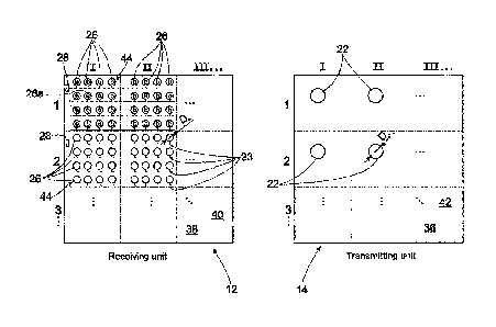
Fig. 1 shows the structure of the transmitting unit 14 and the receiving unit
again in
more detail in a schematic drawing. The transmitting unit in this case has a
plurality of
emitter elements 22, which are implemented here as VCSELs. Only four emitter
elements 22 are shown, although the chip can accommodate many times more
emitter elements. The emitter elements are arranged in a rectangular pattern
on the
plane of the transmitting unit 14. This arrangement in columns and rows is
selected as
an example. For example, the arrangement can also be implemented on the plane
in a
hexagonal pattern or in any other form. The transmitting unit is implemented
as a
focal plane array. Accordingly, the emitter elements 22 are arranged on a
plane 36, in
this case on a chip 42 which forms the plane 36. The plane 36 of the LIDAR
measuring
system 10 is arranged at the focal point of the transmitting lens 18. In
particular, the
emitter elements 22 are arranged in the focal plane of the transmitting lens
18.
The receiving unit 12 has a plurality of sensor elements 26, wherein for the
sake of
clarity only some sensor elements 26 in the figure are labelled with reference
signs.
These transmitting elements, in this case SPADs 26, are also arranged in a
plane 38
which is provided by the chip 40. This plane 38, in particular the sensor
elements 26,
is also arranged on the LIDAR measuring system 10 as a focal plane array in
the focal
plane of the receiving lens 16. The number of sensor elements 26 is
substantially
greater than the number of the emitter elements 22. In this design variant, an
emitter
element 22 has 16 sensor elements 26. A first sensor element 26a is assigned
in each
case to the spatial configuration of an emitter element 22 of the transmitting
unit 14.
In other words, the receiving unit 12 is a copy of the transmitting unit, with
the
Date Recue/Date Received 2023-12-04
19
emitter elements 22 replaced by first sensor elements 26a. Comparing the
emitter
elements with the sensor elements, it is apparent that the VCSELs are larger
in
diameter than the SPADs. The emitter elements 22 have a diameter De and the
sensor
elements 26 have a diameter Ds. Nevertheless, a gap is present on the
transmitting
unit between the adjacent emitter elements 22.
This gap is filled on the receiving unit 12 by additional sensor elements 26,
which are
referred to hereafter as second sensor elements 26b. The reference sign 26b is
shown
for clarity simply as "b" within the drawing of the sensor elements 26 and
only for the
topmost row. The reference signs of the first row accordingly represent the
other
rows and also columns. These second sensor elements 26b are arranged in the
spaces
between the first sensor elements 26a. The second sensor elements 26b are
essentially arranged around the first sensor element 26a.
By using a larger number of sensor elements 26 than the number of emitter
elements
22, imaging errors in the lenses 16 and 18 or other effects can be
compensated. An
emitter element 22 has a larger surface area than a sensor element 26. This
means
that some of the sensor elements 26 on the receiving unit 12 are struck by an
incident
laser light completely, others only partially and others not at all. An
example of this is
shown for a single sensor element in Fig. 3. In the left-hand illustration, a
complete
overlap of the laser light 24 with the sensor element 26 is shown, in the
middle
drawing a partial overlap is shown and in the right-hand illustration a small
overlap.
The diameter DI of the laser light 24 relative to the area of the sensor
element 26 is
only shown schematically. Normally, the diameter DI of the laser light 24 is
so large
that even a multiplicity of sensor elements 26 can be covered with incident
light.
The sensor elements 26 are arranged in macro cells 44. Each macro cell on the
receiving unit 12 is demarcated from a spatially adjacent macro cell 44 by a
dashed
line. Each emitter element 22 is assigned to such a macro cell 44. As an
example, the
corresponding division is also illustrated by dashed lines on the transmitting
unit 14.
The macro cells are divided into columns by Roman numerals I, II, Ill, IV, V,
etc. and
into rows by Arabic numerals, 1, 2, 3, 4, 5, etc. A transmitting unit 14 and a
receiving
unit 12 can have more than 200 rows and columns.
Date Recue/Date Received 2023-12-04
20
Each macro cell has at least one first sensor element 26a and at least one
second
sensor element 26b. These sensor elements 26, which are grouped together in
the
macro cell, are connected to a readout element 28. The readout element detects
an
incoming photon at a sensor element 26 and forwards this to an evaluation
unit, in
particular to a storage unit. The remaining sequence in the processing of the
detected
photons is not explained here.
It is evident that the readout element is connected to all sensor elements 26
of the
macro cell 44. The sensor elements can all be activated individually. This is
effected by
a bias voltage that can be applied to the SPAD. If the bias voltage exceeds a
specific
value, then the SPAD is active. A corresponding lowering below this value
deactivates
the SPAD. The voltage is specified by the control unit, which is connected to
each of
the SPADs. The interconnection is illustrated by conductors 23 by way of
example. For
the sake of clarity this is only implemented in row 2 of the receiving unit.
Accordingly,
only some of the reference signs 23 are drawn in Fig. 1. Each sensor element
26 can
be activated and deactivated independently of the other sensor elements 26.
Thus, only the sensor elements 26 which are also illuminated by the laser
light 24 are
activated. This reduces background noise caused by the ambient radiation,
because
only the sensor element illuminated by the laser light 24 can provide
meaningful
measurements. In addition, by targeted selection of the active sensor elements
26,
imaging errors in the lenses can be corrected. Moreover, other effects that
cause a
displacement of the laser beam 24 relative to the first sensor element 26a can
also be
compensated.
The sensor elements 26 can also be combined into groups for activation and
deactivation, so that these groups can be activated and deactivated
simultaneously.
These can be, for example, subsets of sensor elements 26 of a macro cell 44 or
all
sensor elements 26 of a macro cell 44.
The readout element 28 on the receiving unit 12 in Fig. 1 is formed in each
line of
macro cells 44 and is connected to all sensor elements 26 of this particular
line. This
arrangement is only one example, however. In principle, each sensor element
can
have its own readout element. It is particularly advantageous if each line of
sensor
elements has one readout element. As an example, two adjacent rows can have a
Date Recue/Date Received 2023-12-04
21
common readout element 28, wherein each sensor element 26 of the row is
connected to this readout element 28. The sensor element 28 is also connected
to a
plurality of sensor elements 26 of different macro cells 44 of a row.
As an example, in this design of the receiving unit a horizontal scanning
process is
performed. Alternatively, vertical or diagonal scanning processes, in addition
to other
sequences such as rotating or even random scanning processes, are also
possible. The
emitter elements of column I emit a laser light 24 first and the desired
sensor
elements 26 of column I are activated simultaneously. The readout elements 28
can
process incident laser light 24. On the completion of a measuring cycle, the
sensor
elements of column I are deactivated and the same operation begins for column
II,
etc. Since the readout unit 28 can only read out measurement data from
activated
sensor elements 26 or active macro cells 44, it is possible to use a single
readout unit
28 for a plurality of consecutively active macro cells 44 or sensor elements
26.
However, this arrangement and procedural description is only exemplary, and a
wide
range of arrangement options and scanning variants are possible for the
receiving
unit.
The sensor elements of the simultaneously active macro cells in a first
measuring
cycle for column I are connected to different readout elements 28 one macro
cell at a
time. Nevertheless, a simultaneous connection of sensor elements 26 to one
readout
element 28 exists in macro cells 44 which are not active at the same time,
i.e. are in
adjacent lines.
In Fig. 1 it is also apparent that essentially no space is formed between the
sensor
elements 26 of two vertically adjacent macro cells 44, while a space is formed
between two horizontally adjacent macro cells 44. This spacing provides
assembly
space for the arrangement of additional electronic components. A space is
formed
between the sensor elements of column I and column II. No space is formed
between
the sensor elements of row 1 and row 2. The spacing of a macro cell is derived
from
the spacing of the sensor elements of these macro cells.
Fig. 4 shows a square arrangement of sensor elements 26 as an example. Here,
the
laser light in Fig. 4a, which is illustrated by the circle with the reference
sign 24, strikes
the centre of a macro cell 44. The laser light incident in a circular pattern
has a
Date Recue/Date Received 2023-12-04
22
diameter DI, so that in this case four circular sensor elements 26 are covered
by the
laser light. This represents the theoretical point of incidence of the laser
light on the
receiving unit 12 if the light is reflected on an object at infinity. The four
dark hatched
or filled sensor elements 26x are activated and the sensor elements 26 shown
as
unfilled circles 26y are deactivated. In contrast to the non-activated sensor
elements
26y, the activated sensor elements 26x are almost completely covered with
laser light,
so that an optimal signal-to-noise ratio is achieved. If the deactivated
sensor elements
26y were also activated, only the signal to noise ratios would deteriorate.
Fig. 4b shows the same configuration as in Fig. 4a. Due to an example imaging
error in
the receiving lens the laser light impinges on the receiving unit with an
offset. The
incident laser light 24 is thus displaced compared to Fig. 4a. Instead of the
four
illuminated sensor elements 26, only two sensor elements 26x are now
illuminated
fully and a third sensor element 26x at least to a large extent. One of the
previously
active sensor elements 26 has been deactivated to maintain an optimal signal-
to-
noise ratio. Any imaging errors of the lenses can differ from macro cell to
macro cell
and can be compensated by activating the correct sensor elements 26.
In another variant, shown in Fig. 5, a hexagonal pattern is used for the
sensor
elements 26. The hexagonal pattern or the hexagonal arrangement of the sensor
elements 26 achieves a higher filling density, but on the other hand the
number of
active sensor elements 26x is reduced to 3. However, the diameter DI of the
laser
beam is already less than in the embodiments of Fig. 4. Fig. 5a shows the
optimum,
theoretically perfect illumination of three sensor elements, Fig. 5b shows a
small
displacement due to imaging errors so that one sensor element is fully
illuminated
and the other two active sensor elements are illuminated, at least to a large
extent.
Fig. 5c shows poor illumination in this system variant, in which two active
sensor
elements 26x are fully illuminated by the laser light 24 and two deactivated
sensor
elements are only approximately half-illuminated.
In addition, Fig. 6 shows another variant with a hexagonal pattern, in which
the laser
of diameter DI of the laser light is reduced again compared to the embodiments
in
Figs. 4 and 5. The result of this is that one or two of the sensor elements
26x is/are
always sufficiently illuminated and therefore active.
Date Recue/Date Received 2023-12-04
23
Fig. 7 shows another practical example in a schematic representation with
essentially
hexagonally shaped sensor elements 26 arranged in a hexagonal pattern. In this
case a
chip 40 is shown with the sensor elements 26 and the incident laser light. In
the
optimal position of the incident laser light 24, two sensor elements 26x are
activated
and advantageously almost completely illuminated. A hypothetical maximum
expected deviation of the laser light is indicated by the circle with
reference sign 24a,
within which the laser light can impinge on the macro cell 44. It is clear
that the
deactivated sensor elements 26y are arranged around the activated sensor
elements
26x, the activated sensor elements 26x in this case being first sensor
elements 26a
and the deactivated sensor elements 26y being second sensor elements 26b. The
sensor elements 26 and their intermediate spaces form a detector surface,
thereby
essentially covering the area of the laser light including a possible
deflection due to
interference effects. In this example, a diameter Dd of the detector surface
corresponds essentially to twice the diameter DI of the laser light 24,
wherein the
detector surface is arranged centrally with respect to the optimal point of
incidence of
the laser light or centrally around the first sensor elements 26a. The area of
the circle
24a, which also corresponds substantially to the detector surface, is about
four times
as large as the area of the laser light 24. The detector surface generally has
a diameter
Dd of at least 1.2, 1.4, 1.6, 1.8 or 2 times the diameter DI of the laser
light.
Accordingly, the detector surface essentially has an area at least 1.5, 2, 3
or 4 times
the area of the incident laser light.
Corresponding ratios for the areas and for the diameters also apply
correspondingly
to the previous exemplary embodiments, in particular to Figures 4 to 6.
Fig. 8 again shows another variant, in which an even smaller laser beam is
used
compared to Fig. 7 and the arrangement of the sensor elements has a hexagonal
shape. In this case, there is also a horizontal and a vertical gap between the
sensor
elements 26 of two macro cells 44 on the chip 40. This creates additional
space for
further electronics. The remainder of the design corresponds essentially to
the above
statements in the description of the figures.
Date Recue/Date Received 2023-12-04
24
Reference signs
LIDAR measuring system
12 LIDAR receiving unit
14 LIDAR transmitting unit
16 receiving lens
18 transmitting lens
object
22 emitter element, VCSEL
23 cable
24 laser light, pulse
24a circle, hypothetical deviation of laser light
beam
26 sensor element, SPAD
26a first sensor element
26b second sensor element
26x active sensor element
26y deactivated sensor element
28 readout element
evaluation unit
32 control unit
34 connection
36 plane of transmitting unit
38 plane of receiving unit
chip of the receiving unit
42 chip of the transmitting unit
44 macro cell
DI diameter of laser light
Dd diameter of detector surface
De diameter of emitter element
Ds diameter of sensor element
Date Recue/Date Received 2023-12-04