Note : Les descriptions sont présentées dans la langue officielle dans laquelle elles ont été soumises.
CA 03087650 2020-07-03
WO 2019/185973 PCT/F12019/050130
1
Exit pupil expander
Field of the Invention
The invention relates to diffractive display technology. In particular, the
invention relates to
lightguide-based diffractive display elements comprising an exit pupil
expander (EPE).
Such display elements can be used in personal displays, such as head-mounted
displays
(HMDs), for example near-to-eye displays (NEDs), and head-up displays (HUDs).
Background of the Invention
HMDs and HUDs can be implemented using waveguide technology. Light can be
coupled
to a waveguide, redirected therein and coupled out of the waveguide using
diffraction
gratings. In one conventional display design, light is directed from a
projector to an in-
coupling grating, which diffracts the incoming light into the waveguide, where
it
propagates via total internal reflections towards an out-coupling grating via
an EPE grating
to extend the viewable area of the display laterally. EPEs typically comprise
a grating
which has grating lines oblique with respect to the grating line orientation
of the in-
coupling grating and the propagation direction of light incoming from the in-
coupling
grating.
Like all gratings, also EPE gratings generally cause losses and disturbances.
This
decreases the brightness and uniformity of the final image formed and causes
image
imperfections, such as colour imbalance.
Thus, there is a need for improved exit pupil expansion solutions and improved
waveguide
displays.
Summary of the Invention
It is an aim of the invention to increase the image quality of waveguide
displays. Particular
aims are to increase the brightness (total efficiency), uniformity and/or
color balance of
waveguide displays. One aim is to provide an EPE solution that relieves
geometric
constraints of EPE shapes.
CA 03087650 2020-07-03
WO 2019/185973 PCT/F12019/050130
2
The aim is achieved by the what is stated in the independent claims.
According to one aspect, there is provided an exit pupil expander (EPE) for
use in a
diffractive display, the EPE comprising a plurality of diffractive zones
(grating zones) on a
waveguide and a plurality of non-diffractive zones (non-grating zones) between
at least
some of the diffractive zones. The diffractive zones and non-diffractive zones
can be
arranged as an irregular or regular two-dimensional pattern.
In other words, there is provided an EPE having an area containing a plurality
of diffractive
zones and "voids" at which no diffraction, but only total internal reflection
from a surface of
the waveguide takes place.
According to one aspect, there is provided a diffractive display element for
personal
displays, the element comprising a waveguide, an in-coupling region for
diffractively
coupling an image into the waveguide body, an out-coupling region for
diffractively
coupling the image out of the waveguide body, and an exit pupil expander (EPE)
region of
the presently disclosed kind between the in-coupling region and the out-
coupling region
for expanding the exit pupil of the image on the out-coupling region.
According to one aspect, there is provided a personal display device, such as
a head-
mounted display (HMD) or head-up display (HUD), comprising a diffractive
display
element of the above kind.
EPE herein means a region in the lateral plane of the waveguide that has the
property of
extending the exit pupil of light incoming from one lateral direction and
outgoing to another
lateral direction.
The invention offers significant benefits. The inclusion of voids inside and
on the
peripheral boundary of the EPE region enables the optimization of
geometrically more
complex EPEs. Typically, the EPE shape is calculated by simple geometrical
calculations
using rays propagating with extreme angles inside the waveguide. This leads to
a non-
optimal solution. The present invention helps to find EPE solutions via
numerical
optimization that exhibit better performance in terms of color balance and
efficiency than
the EPE shapes calculated by simple geometrical calculations. The approach can
be used
also to find EPE structures that allow more compact form factor for the
waveguide.
Especially, large field of view (>40 deg) EPEs tend to grow so large that the
total
waveguide size is too big for wearable displays with compact form factor.
CA 03087650 2020-07-03
WO 2019/185973 PCT/F12019/050130
3
The dependent claims are directed to selected embodiments of the invention.
In some embodiments there is at least one first non-diffractive zone is
positioned between
two diffractive zones in a first direction and at least one second non-
diffractive zone is
positioned between two diffractive zones in a second direction orthogonal to
the first
direction. In some embodiments there are at least 10 different (separate)
diffractive zones
and at least 10 different (separate) non-diffractive zones.
In some embodiments there are at least two diffractive zones and/or at least
two non-
diffractive zones with different sizes or shapes.
In some embodiments the diffractive zones comprise at least two zones with
different
grating properties. This allows for performing even more complex EPE
functions.
In some embodiments the diffractive zones and non-diffractive zones are
dividable in the
surface plane of the waveguide into equally shaped unit zones.
In some embodiments at least 20% of the total area of the EPE is formed of non-
diffractive zones.
In some embodiments the zones are positioned such that it is possible to draw
at least
two different cross-sectional lines in along both main optical axes thereof so
that the
diffractive/non-diffractive profile along those lines is different.
In some embodiments, in the present waveguide element the diffractive zones
and non-
diffractive zones of the EPE are configured so that at least a majority of
light incoming
.. from the in-coupling region is diffracted by at least one diffractive zone,
bounced by total
internal reflection in at least one non-diffractive zone, and again diffracted
by at least one
diffractive zone, typically different from the first diffractive zone, before
exiting the EPE
towards the out-coupling region.
In some embodiments the non-diffractive zones of the EPE are provided therein
for
increasing the brightness, uniformity or color balance of the display element,
compared
with a situation where the non-diffractive zones were replaced with
diffractive zones.
In some embodiments, the EPE has a width which is at least the same as the
width of the
out-coupling region.
CA 03087650 2020-07-03
WO 2019/185973 PCT/F12019/050130
4
Next, embodiments of the invention and advantages thereof are discussed in
more detail
with reference to the attached drawings.
Brief Description of the Drawings
Fig. 1 shows an network of ray pats formed inside an EPE structure due to a
single
incident ray.
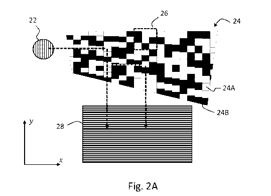
Fig. 2A shows an exemplary EPE in accordance with the invention, positioned
optically
between an in-coupler and an out-coupler.
Fig. 2B shows a detail view of a portion of the EPE of Fig. 2A.
Detailed Description of Embodiments
When a light ray propagates through EPE, a complex network of ray paths is
formed, in
which energy flows typically along two directions. An exemplary network is
shown in Fig 1.
The dots show the locations where the rays, generated due to diffraction from
the incident
ray 11, hit the grating surface. The network structure allows energy transport
along
multiple ray paths between the points inside the network. Two example paths
are shown
by dashed lines from the point A to B. As all possible paths are not needed
for energy
transport, the operation of the EPE structure can be enhanced by allowing also
empty
regions (voids) to be formed inside EPE and on the peripheral boundary of EPE
during
numerical optimization.
Fig. 2A shows an in-coupling grating 22 to which light is directed from a
projector, typically
essentially perpendicular to the image plane of the figure. Light is
diffracted and
propagates in the waveguide to the EPE 24 comprising diffractive zones 24A and
non-
diffractive zones (voids) 24B. The non-diffractive zones 24B are typically
simply regions
without a grating pattern therein, whereas the diffractive zones comprise a
grating. The
non-diffractive zones therefore serve as an ordinary waveguide zone, where
light rays
bounce via total internal reflections without diffraction.
The diffractive zones 24A typically comprise a linear (one-dimensional)
grating pattern.
The orientation of grating lines and period of grating between each
diffractive zones 24A
is typically the same, while the microfeature profile, including in particular
fill factor and/or
height of microfeatures, may differ between the zones.
CA 03087650 2020-07-03
WO 2019/185973 PCT/F12019/050130
The diffractive zones 24A may be unit zones, for example rectangular unit
zones like
shown in Fig. 2A, or arbitrarily shaped zones without unitary grating lines
therein (that is,
without the inner boundaries drawn in Figs. 2A and 2B).
The invention is not restricted to orthogonal geometry as concerns the shapes
of the
5 diffractive zones 24A and non-diffractive zones 24B. They can have
oblique or curved
outer shapes of practically any complexity.
The positioning of the diffractive zones and non-diffractive zones can be
determined and
optimized using computational techniques known per se for diffractive optical
design.
The in-coupling grating 22, EPE 24 and out-coupling grating are typically
arranged on a
planar waveguide element. The waveguide can be a planar piece of transparent
material,
typically plastic or glass, having two parallel main surfaces. All gratings
and diffractive
zones discussed here can be fabricated for example as surface relief gratings
(SRGs) or
by providing additional material onto the surface as diffractive features, or
other diffractive
optical elements (DOEs). In one example, the gratings comprise linear features
made of
at least one oxide or nitride material, such as TiO2, Si3N4, and Hf02, on a
glass
waveguide.
It should be noted that the invention is applicable also in various other
display geometries
and configurations.
In the case of multilayer waveguides, each layer carrying for example a
different
wavelength band, embodiments of the invention can be applied separately to
each layer.
Embodiments of the invention are usable both with broadband illumination and
narrowband (including narrow multi-band) illumination and projectors.