Note : Les descriptions sont présentées dans la langue officielle dans laquelle elles ont été soumises.
CA 03087661 2020-07-03
DESCRIPTION
IC TAG
Technical Field
[0001] The present invention relates to an IC tag.
Background Art
[0002] In recent years, a type of IC tag called an "inlet"
has been proposed, in which an antenna pattern for radio
frequency communication and an IC chip are mounted on a
base sheet made of plastic or paper. Such inlets are used
for the management of articles in a state of being sealed
with resin and then attached to or embedded in the
articles.
[0003] The above-described IC tags may be attached to linen
articles for management of the linen articles, but it is
common practice to use a metal detector to inspect the
linen articles for the presence of metal contaminants at
the time of shipment. However, the IC tags have an antenna
pattern formed of metal, and thus, when a metal detector is
used to inspect the linen articles having the IC tags
attached thereto, the metal detector detects the IC tags as
metal even if no metal contaminants are present in the
linen articles. This poses a problem in that the
inspection for actual metal contaminants cannot be
performed smoothly.
[0004] To address this problem, Patent Literature 1
1
Date Recue/Date Received 2020-07-03
CA 03087661 2020-07-03
discloses an IC tag in which the resistance value of an
antenna is set to 50 to 1000 S-2, and also discloses that the
IC tag with an antenna resistance value in such a range
does not respond to a metal detector.
Citation List
Patent Literature
[0005] Patent Literature 1: JP 2016-33748A
Summary of Invention
Technical Problem
[0006] However, even the IC tag of Patent Literature 1 may
be detected by a metal detector, and further improvement
thus has been demanded. The present invention is intended
to solve the above-described problem, and it is an object
of the present invention to provide an IC tag that can be
more reliably prevented from being detected by a metal
detector.
Solution to Problem
[0007] The IC tag according to the present invention is an
IC tag including: an IC chip; a dipole antenna for
electrically transmitting and receiving information stored
in the IC chip; and a sheet-shaped substrate that supports
the IC chip and the dipole antenna, wherein 0.1 R/L 2.5
is satisfied, where R is a resistance value between two
ends of the dipole antenna and L is a length of a path that
2
Date Recue/Date Received 2020-07-03
CA 03087661 2020-07-03
connects the two ends of the dipole antenna while extending
along the dipole antenna without passing through the IC
chip.
[0008] In the above-described IC tag, the length L may be
not less than 120 mm and not more than 200 mm.
[0009] In the above-described IC tag, the material of the
dipole antenna may contain any one of silver, aluminum, and
copper.
[0010] The above-described IC tag may further include: a
sheet-shaped cover that covers the IC chip and the antenna,
the IC chip and the antenna being disposed between the
cover and the substrate; and a pressure-sensitive adhesive
that bonds the cover and the substrate.
Advantageous Effects of Invention
[0011] According to the present invention, it is possible
to more reliably prevent an IC tag from being detected by a
metal detector.
Brief Description of Drawings
[0012] FIG. 1 is a plan view showing an embodiment of an IC
tag according to the present invention;
FIG. 2 is a cross-sectional view of the IC tag shown
in FIG. 1;
FIG. 3 is a plan view for illustrating an antenna of
the IC tag shown in FIG. 1;
FIG. 4 is a plan view showing the shape of a dipole
3
Date Recue/Date Received 2020-07-03
CA 03087661 2020-07-03
antenna used in Example 1 and Comparative Example 1;
FIG. 5 is a plan view showing the shape of a dipole
antenna used in Example 2;
FIG. 6 is a plan view showing the shape of a dipole
antenna used in Example 3 and Comparative Example 2;
FIG. 7 is a plan view showing the shape of a dipole
antenna used in Example 4; and
FIG. 8 is a plan view showing the shape of a dipole
antenna used in Example 5.
Description of Embodiments
[0013] 1. Overview of IC tag
An embodiment of an IC tag according to the present
invention will be described below with reference to the
drawings. FIG. 1 is a plan view of the IC tag according to
the present embodiment, and FIG. 2 is a cross-sectional
view of FIG. 1. FIG. 1 does not show a cover for the sake
of convenience of illustration. As shown in FIGS. 1 and 2,
the IC tag according to the present embodiment includes a
sheet-shaped substrate 1 formed in a rectangular shape, an
IC chip 2 and a dipole antenna 3 disposed on this substrate
1, and a sheet-shaped cover 4 that is formed in a
rectangular shape and covers the IC chip 2 and the dipole
antenna 3. The substrate 1 and the cover 4 are bonded
together using a pressure-sensitive adhesive 5. Each of
these members will be described in detail below.
[0014] The substrate 1 and the cover 4 are formed in the
4
Date Recue/Date Received 2020-07-03
CA 03087661 2020-07-03
same shape, and the pressure-sensitive adhesive 5 is
disposed so as to completely fill the gap between the
substrate 1 and the cover 4. That is, the pressure-
sensitive adhesive 5 covers the IC chip 2 and the dipole
antenna 3 in such a manner that the IC chip 2 and the
dipole antenna 3 are not exposed from the gap between the
substrate 1 and the cover 4.
[0015] The materials of the substrate 1 and the cover 4 are
not particularly limited, and, for example, may be formed
using polyethylene, polypropylene, polyethylene
terephthalate, polyvinyl chloride, or the like. The
thicknesses of the substrate 1 and the cover 4 are, for
example, preferably 25 to 200 pm and more preferably 25 to
100 pm.
[0016] Hereinafter, as shown in FIG. 1, sides of the
substrate 1 and the cover 4 in the lengthwise direction are
referred to as a first side 101 and a second side 102, and
sides of the same in the widthwise direction are referred
to as a third side 103 and a fourth side 104, for the sake
of convenience of explanation. Accordingly, these sides
are connected to each other in the order of the first side
101, the third side 103, the second side 102, and the
fourth side 104.
[0017] The IC chip 2 is a known IC chip having a memory
function, and is electrically connected to the dipole
antenna 3 formed of a conductor.
[0018] In the present embodiment, a dipole antenna as shown
5
Date Recue/Date Received 2020-07-03
CA 03087661 2020-07-03
in FIG. 1 is used as an illustrative example.
Specifically, this dipole antenna 3 includes an impedance
matching portion 31 disposed in the vicinity of the center
of the substrate 1 in the lengthwise direction, and a pair
of dipole portions 32 extending from the impedance matching
portion 31 in the lengthwise direction of the substrate 1.
The impedance matching portion 31 is formed in the shape of
a rectangular frame having first to fourth sides. More
specifically, a first side 311 of the impedance matching
portion 31 is disposed somewhat spaced apart from the first
side 101 of the substrate 1, and a second side 312 is
disposed along the second side 102 of the substrate 1.
That is, in the impedance matching portion 31, the first
side 311, a third side 313, the second side 312, and a
fourth side 314 are connected to each other in this order.
The IC chip 2 is disposed in the vicinity of the center of
the first side 311 of the impedance matching portion 31.
[0019] Since the dipole portions 32 have shapes symmetrical
to each other, only one of them will be described. The
dipole portion 32 extends from the first side 311 of the
impedance matching portion 31 toward the first side 101 of
the substrate 1, then extends along the first side 101, the
third side 103, and the second side 102 of the substrate 1,
and further extends along the third side 313 of the
impedance matching portion 31, thereby forming a
rectangular frame. Thereafter, the dipole portion 32
extends spirally inside the frame.
6
Date Recue/Date Received 2020-07-03
CA 03087661 2020-07-03
[0020] The material of the dipole antenna 3 is not
particularly limited, and the dipole antenna 3 can be made
of, for example, silver, copper, or aluminum. When silver
is used, the dipole antenna 3 can be formed by applying a
silver paste containing silver onto the substrate 1 through
screen printing. On the other hand, when copper or
aluminum is used, the dipole antenna 3 can be formed
through etching. The IC chip 2 can be fixed to the antenna
3 using, for example, a known flip-chip mounting procedure
for electronic components.
[0021] The above-described dipole antenna 3 enables
transmission and reception of information stored in the IC
chip 2 using, for example, radio waves in the UHF band.
[0022] The pressure-sensitive adhesive 5 may be, for
example, a rubber-based pressure-sensitive adhesive
containing natural rubber or synthetic rubber as a main
component. The thickness of the rubber-based pressure-
sensitive adhesive 5 is not particularly limited, and is
preferably 28 to 500 pm and more preferably 28 to 72 pm.
Examples of the synthetic rubber to be used in the rubber-
based pressure-sensitive adhesive 5 include, but not
particularly limited to, styrene-isoprene-styrene block
copolymers, styrene-butadiene-styrene block copolymers,
hydrogenated products of the above-described styrene-based
block copolymers, styrene-butadiene rubber (SBR),
polyisoprene rubber (IR), polyisobutylene (PIB), and butyl
rubber (IIR).
7
Date Recue/Date Received 2020-07-03
CA 03087661 2020-07-03
[0023] The rubber-based pressure-sensitive adhesive 5 may
further contain a tackifier, in addition to the above-
described natural rubber or synthetic rubber. Examples of
the tackifier include terpene phenol resins, rosin resins,
and petroleum resins. The amount of resin to be used as
the tackifier can be selected as appropriate within a range
where the pressure-sensitive adhesion performance is not
impaired. In addition to the above-described components,
the rubber-based pressure-sensitive adhesive may optionally
contain additives such as a softener, a plasticizer, a
filler, an anti-aging agent, and a coloring agent as
necessary.
[0024] As the pressure-sensitive adhesive 5, not only the
rubber-based pressure-sensitive adhesive but also an
acrylic pressure-sensitive adhesive or a silicone pressure-
sensitive adhesive can be used.
[0025] 2. Physical and Electrical Properties of Dipole
Antenna
The dipole antenna 3 according to the present
embodiment has the following physical and electrical
properties. The physical and electrical properties will be
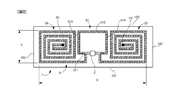
described with reference to FIG. 3. First, as shown in
FIG. 3, the resistance value between two ends Si and S2 of
the dipole antenna 3 is defined as R (W, and the length of
a path that connects the two ends Si and S2 of the dipole
antenna 3 while extending along the dipole antenna 3
without passing through the IC chip 2 (hereinafter, this
8
Date Recue/Date Received 2020-07-03
CA 03087661 2020-07-03
path is referred to as "antenna path": indicated with the
broken line in FIG. 3) is defined as L (cm). The dipole
antenna 3 according to the present embodiment satisfies the
following formula (1). The antenna path passes through the
center of the line width of the dipole antenna 1.
0.1 R/L 2.5 (1)
[0026] This defines the resistance per unit length of the
antenna path. When R/L is 0.1 or more, it becomes
difficult for a current to flow, whereby the IC tag is
prevented from being detected by a metal detector. On the
other hand, when R/L is greater than 2.5, the communication
range is reduced, whereby application software to which the
IC tag is applicable may be limited. Accordingly, R/L is
preferably 2.5 or less. In order to more reliably prevent
the IC tag from being detected by a metal detector, it is
more preferable that R/L satisfies the following formula
(2).
1.5 R/L 2.5 (2)
[0027] The resistance value R (Q) between the two ends Si
and S2 of the antenna 3 is not particularly limited, and
is, for example, preferably 10 to 50 Q and more preferably
20 to 44 Q. This is because, when the resistance value R
is 10 Q or more, it becomes difficult for a current to
flow, and when the resistance value R is 50 Q or less, the
communication range is broad enough to stabilize
communication.
[0028] Also, the length L of the above-described antenna
9
Date Recue/Date Received 2020-07-03
CA 03087661 2020-07-03
path is not particularly limited, and is, for example,
preferably 120 to 200 mm and more preferably 130 to 180 mm.
This is because, when the length L of the antenna path is
short, the communication becomes unstable, and when the
antenna path is too long, the IC tag is more likely to be
detected by a metal detector.
[0029] The size of the outer shape of the dipole antenna 3
is not particularly limited. In order to prevent the IC
tag from being detected by a metal detector, the length X
of the outer shape of the dipole antenna 3 in the
lengthwise direction is, for example, preferably 60 mm or
less and more preferably 40 mm or less. The length Y of
the outer shape of the dipole antenna 3 in the widthwise
direction is preferably 20 mm or less and more preferably
10 mm or less. Accordingly, the area (X x Y) of the outer
shape of the dipole antenna is preferably 1200 mm2 and more
preferably 400 mm2 or less.
[0030] The thickness of the dipole antenna 3 is not
particularly limited, and is, for example, preferably 20 pm
or less, more preferably 15 pm or less, and particularly
preferably 10 pm or less. For example, when the dipole
antenna 3 is formed through printing the above-described
silver paste, the thickness of the dipole antenna 3 can be
adjusted more easily as compared with the case where the
dipole antenna 3 is formed using copper or aluminum through
etching, and the thickness of the dipole antenna 3 can be
set to 10 pm or less. Accordingly, the IC tag can be more
Date Recue/Date Received 2020-07-03
CA 03087661 2020-07-03
reliably prevented from being detected by a metal detector.
[0031] 3. Metal Detector
A metal detector by which the IC tag according to the
present embodiment should not be detected may be, for
example, a metal detector for detecting nonferrous metals.
This is because, as described above, there are cases where
the dipole antenna is formed of a nonferrous metal such as
silver, copper, or aluminum. The detection sensitivity is
preferably such that the IC tag is not detected when, for
example, MUK-500 manufactured by NIKKA DENSOK LIMITED is
used as a metal detector. This device has a detection
sensitivity capable of detecting, as the smallest substance
it can detect, a ball made of SUS having an outer diameter
of 1.5 mm or more. Therefore, as an example of the metal
detector by which the IC tag according to the present
embodiment is not detected, a metal detector having the
above-described detection sensitivity for nonferrous metals
can be defined. It is to be noted, however, that such a
metal detector is merely an illustrative example, and the
present invention may be embodied based on the assumption
that the metal detector is a metal detector for detecting
iron.
[0032] 4. Characteristics
As described above, the IC tag according to the
present embodiment in which the dipole antenna 3 is
configured to satisfy the above formula (1) can be
prevented from being detected by a metal detector.
11
Date Recue/Date Received 2020-07-03
CA 03087661 2020-07-03
[0033] 5. Modifications
Although one embodiment of the present invention has
been described above, the present invention is not limited
to the above embodiment, and various changes can be made
thereto without departing from the gist of the invention.
Moreover, a plurality of modifications to be described
below can be combined as appropriate.
[0034] 5-1
The shape of the above-described dipole antenna 3 is
merely an illustrative example, and various shapes can be
adopted as long as the above formula (1) is satisfied.
Moreover, the shape of the IC tag, i.e., the shapes of the
substrate 1 and the cover 4 are also not particularly
limited. In addition to an elongated shape such as
described above, the IC tag may have various shapes
including a rectangular shape, a circular shape, and a
polygonal shape according to its use. Further, the
substrate 1 and the cover 4 need not have the same shape.
[0035] 5-2
In the above embodiment, the pressure-sensitive
adhesive 5 is applied so as to completely fill the gap
between the substrate 1 and the cover 4. However, the
present invention is not limited thereto. For example, the
rubber-based pressure-sensitive adhesive 5 may be applied
only to a peripheral edge portion of the substrate 1 and
the cover 4 such that the IC chip 2 and the antenna 3 are
surrounded by the pressure-sensitive adhesive 5. The cover
12
Date Recue/Date Received 2020-07-03
CA 03087661 2020-07-03
4 and the pressure-sensitive adhesive 5 are not essential
and may be omitted.
Examples
[0036] Examples of the present invention will be described
below. However, the present invention is not limited to
the following examples.
[0037] 1. Preparation of Examples and Comparative Examples
IC tags according to Examples 1 to 5 and Comparative
Examples 1 and 2 were prepared as follows. The IC tags of
these examples and comparative examples used the same
substrate and IC chip, but dipole antennas used therein
were different from each other. Antennas of five types of
shapes as shown in FIGS. 4 to 8 were prepared, and antennas
of three types of materials were prepared. In FIGS. 4 to
8, the dotted line indicates the path L, and the numerical
values indicate the lengths X and Y of the outer shape. As
the substrate and a cover of each IC tag, polyethylene
terephthalate films having a thickness of 50 pm were
prepared. The dipole antenna was disposed between the
substrate and the cover, and fixed using the above-
described rubber-based pressure-sensitive adhesive. Then,
the IC tags according to Examples 1 to 5 and Comparative
Examples 1 and 2 were prepared as shown in Table 1 below.
As described below, the antennas of the examples and the
comparative examples were each made of a nonferrous metal.
13
Date Recue/Date Received 2020-07-03
[Table 1]
Path
Resistance
Minimum Length Length
Volume
Shape Material Thickness Length
Area R at two R/L
width X(1) y(2)
resistivity
of of L
ends
antenna antenna
(mm) (mm) (cm) (mm) (mm)
(mm2) (am) (0)
Silver
Ex. 1 FIG. 4 0.005 0.5 17.0 25 7.5 188
5.31 x 10⁻⁷ 36.1 2.12
paste
Silver
Ex. 2 FIG. 5 0.005 0.5 17.4 30 7.5 255
5.95 x 10⁻⁷ 41.4 2.38
paste
Silver
P
Ex. 3 FIG. 6 0.005 0.55 13.7 39 7.5 293
4.46 x 10⁻⁷ 22.2 1.62 0
w
paste
0
m
..J
m
Silver
m
Ex. 4 FIG. 7 0.015 0.72 14.1 53 4 212
1.53 x 10⁻⁷ 2 0.14 1-
I.,
paste
0
I.,
0
1
Silver
0
Ex. 5 FIG. 8 0.015 0.72 12.8 55 6 330
1.53 x 10⁻⁷ 1.8 0.14 ..J
1
0
paste
w
Comp.
FIG. 4 Aluminum 0.01 0.5 17.0 25 7.5 188
2.65 x 10⁻⁸ 0.9 0.05
Ex. 1
Comp.
FIG. 6 Copper 0.018 0.55 13.7 39 7.5 293
1.73 x 10⁻⁸ 0.24 0.018
Ex. 2
(1) Length X in lengthwise direction
(2) Length Y in widthwise direction
14
Date Recue/Date Received 2020-07-03
CA 03087661 2020-07-03
[0038] 2. Evaluation
Using MUK-500 manufactured by NIKKA DENSOK LIMITED as
a metal detector, whether the metal detector could detect
the IC tags according to the above-described examples and
comparative example was examined. The detection levels in
this device are 0 to 12. Specifically, the detection
levels are as follows. That is, when balls made of 5U5304
are used, this device cannot detect a ball with a diameter
of 1 mm but can detect a ball with a diameter of 2 mm or
more. The detection level when the device detects a ball
with a diameter of 2 mm is 8, and the detection level when
the device detects a ball with a diameter of 3 mm is 12.
On the other hand, a detection level of 0 means that this
metal detector cannot detect a target substance at all.
That is, the closer the detection level is to 0, the more
difficult it becomes for the metal detector to detect a
target substance.
[Table 2]
Detection Level
Example 1 0
Example 2 0
Example 3 0
Example 4 3
Example 5 3
Comparative Example 1 12
Comparative Example 2 12
Date Recue/Date Received 2020-07-03
CA 03087661 2020-07-03
[0039] In Examples 1 to 3, the R/L values were 1.5 or more,
and the detection levels were all 0. That is, the IC tags
of Examples 1 to 3 were not detected by the metal detector
at all. In Examples 4 and 5, the R/L values were 1 or less
and lower than those in Examples 1 to 3, but were not less
than 0.1. The levels of detection by the metal detector
were 3. That is, although the IC tags of Examples 4 and 5
were slightly detectable, they were acceptable depending on
the intended use thereof. On the other hand, in
Comparative Examples 1 and 2, the R/L values were both
lower than 0.1, and the detection levels were 12. That is,
the IC tags of Comparative Examples 1 and 2 were at the
detection level of certain detection by the metal detector.
Thus, the evaluation based on the R/L values showed that
the IC tags of Examples 1 to 5 are all superior to the IC
tags of Comparative Examples 1 and 2.
List of Reference Numerals
[0040] 1 Substrate
2 IC chip
3 Dipole antenna
4 Cover
5 Pressure-sensitive adhesive
16
Date Recue/Date Received 2020-07-03