Sélection de la langue

Search

Sommaire du brevet 3088408 

Énoncé de désistement de responsabilité concernant l'information provenant de tiers

Une partie des informations de ce site Web a été fournie par des sources externes. Le gouvernement du Canada n'assume aucune responsabilité concernant la précision, l'actualité ou la fiabilité des informations fournies par les sources externes. Les utilisateurs qui désirent employer cette information devraient consulter directement la source des informations. Le contenu fourni par les sources externes n'est pas assujetti aux exigences sur les langues officielles, la protection des renseignements personnels et l'accessibilité.

Disponibilité de l'Abrégé et des Revendications

L'apparition de différences dans le texte et l'image des Revendications et de l'Abrégé dépend du moment auquel le document est publié. Les textes des Revendications et de l'Abrégé sont affichés :

  • lorsque la demande peut être examinée par le public;
  • lorsque le brevet est émis (délivrance).
(12) Brevet: (11) CA 3088408
(54) Titre français: BOUCLES DE STOCKAGE TRI-STABLES
(54) Titre anglais: TRI-STABLE STORAGE LOOPS
Statut: Accordé et délivré
Données bibliographiques
(51) Classification internationale des brevets (CIB):
  • H03K 03/38 (2006.01)
  • G06N 99/00 (2019.01)
  • G11C 11/44 (2006.01)
  • H03K 19/195 (2006.01)
(72) Inventeurs :
  • BRAUN, ALEXANDER LOUIS (Etats-Unis d'Amérique)
(73) Titulaires :
  • NORTHROP GRUMMAN SYSTEMS CORPORATION
(71) Demandeurs :
  • NORTHROP GRUMMAN SYSTEMS CORPORATION (Etats-Unis d'Amérique)
(74) Agent: GOWLING WLG (CANADA) LLP
(74) Co-agent:
(45) Délivré: 2024-01-16
(86) Date de dépôt PCT: 2019-01-25
(87) Mise à la disponibilité du public: 2019-08-08
Requête d'examen: 2020-07-13
Licence disponible: S.O.
Cédé au domaine public: S.O.
(25) Langue des documents déposés: Anglais

Traité de coopération en matière de brevets (PCT): Oui
(86) Numéro de la demande PCT: PCT/US2019/015229
(87) Numéro de publication internationale PCT: US2019015229
(85) Entrée nationale: 2020-07-13

(30) Données de priorité de la demande:
Numéro de la demande Pays / territoire Date
15/886,652 (Etats-Unis d'Amérique) 2018-02-01

Abrégés

Abrégé français

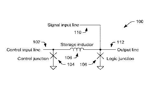
Une boucle de stockage tri-stable utile dans des circuits et des systèmes de grille à logique quantique inverse (RQL) comprend des lignes de commande et d'entrée de signal. Lorsque des états de stockage de courant stables alternés sont induits dans la boucle de stockage par une entrée alternative fournie à la ligne d'entrée de commande, la fourniture d'une impulsion SFQ positive sur la ligne d'entrée de signal tandis que la boucle de stockage stocke un courant positif change la boucle de stockage d'une alternance entre un état de courant positif et un état de courant nul à une alternance entre un état de courant négatif et l'état de courant nul, et la fourniture d'une impulsion SFQ négative sur la ligne d'entrée de signal tandis que la boucle de stockage stocke un courant négatif change la boucle de stockage d'une alternance entre l'état de courant négatif et l'état de courant nul à une alternance entre l'état de courant positif et l'état de courant nul.


Abrégé anglais

A tri-stable storage loop useful in reciprocal quantum logic (RQL) gate circuits and systems has control and signal input lines. When alternating stable current storage states are induced in the storage loop by an alternating input provided to the control input line, provision of a positive SFQ pulse on the signal input line while the storage loop stores a positive current changes the storage loop from alternating between a positive-current state and a null current state to alternating between a negative-current state and the null-current state, and provision of a negative SFQ pulse on the signal input line while the storage loop stores a negative current changes the storage loop from alternating between the negative-current state and the null current state to alternating between the positive-current state and the null-current state.

Revendications

Note : Les revendications sont présentées dans la langue officielle dans laquelle elles ont été soumises.


CLAIMS
What is claimed is:
1. A reciprocal quantum logic (RQL) tri-stable storage loop circuit
comprising:
a control input line configured to provide a control input to an input end of
a storage
loop;
a signal input line configured to provide a signal input to an output end of
the storage
loop; and
an output line configured to propagate an output single flux quantum (SFQ)
pulse from
the output end of the storage loop;
wherein the storage loop comprises:
a control Josephson junction (JJ) at the input end;
a logic JJ at the output end; and
a storage inductor connecting the input end to the output end, and
wherein the circuit is configured such that, in the absence of input on the
signal
input line, the storage loop has two stable states including a first stable
state wherein no
current flows in the storage loop and a second stable state wherein one (Do
worth of
current flows in the storage loop, and further wherein the circuit is
configured such that,
upon provision of a positive SFQ pulse to the signal input line, the storage
loop obtains a
third stable state wherein ¨00 worth of current flows in the storage loop.
2. The circuit of claim 1, wherein the storage loop is configured to
selectively apply
positive, negative, and no bias to the logic JJ based on the storage loop
storing positive current,
negative current, and no current, respectively.
3. The circuit of claim 1, wherein the Hs and the storage inductor are
sized to enforce
unidirectional signal flow from the input end to the output end.
8
Date Recue/Date Received 2023-06-07

4. The circuit of claim 3, wherein the control JJ is sized such that:
a driving Josephson transmission line (JTL) connected to the control input
line is capable
of causing the control JJ to trigger to put a current into the storage loop,
and the current is insufficient to cause the control JJ to untrigger to cause
a pulse to back
out of the control input line.
5. The circuit of claim 1, configured such that an SFQ pulse input via the
signal input line
when there is zero current in the storage loop is insufficient to trigger the
logic JJ.
6. The circuit of claim 5, configured such that a positive SFQ pulse input
via the signal
input line when there is positive current in the storage loop causes the logic
JJ to positively
trigger, annihilating the positive current in the storage loop.
7. The circuit of claim 6, configured such that a negative SFQ pulse input
via the signal
input line when there is negative current in the storage loop causes the logic
JJ to negatively
trigger, annihilating the negative current in the storage loop.
8. The circuit of claim 1, wherein, in the absence of input on the signal
input line, the
storage loop has two stable states.
9. The circuit of claim 1, further comprising an AC power source configured
to provide
direct application of AC power supplied along the control input line.
10. The circuit of claim 1, further comprising circuitry configured to
provide one reciprocal
pair of SFQ pulses every AC clock cycle.
11. A method of altering a series of pulses from alternating between a
positive-current state
and a null-current state to alternating between a negative-current state and
the null-current state,
the method comprising:
9
Date Recue/Date Received 2023-06-07

providing alternate positive and negative control inputs to a storage loop in
a reciprocal
quantum logic (RQL) system to alternate the storage loop between
a positive current storage state in which current circulates in the loop in a
positive
direction and
a null current storage state in which substantially no current circulates in
the loop;
and
inputting a positive single flux quantum (SFQ) signal pulse to the storage
loop during the
positive state to
return the storage loop to the null state and subsequently to
cause the storage loop to transition, on the next negative control input, into
a
negative current storage state in which current circulates in the loop in a
negative
direction, whereupon the control inputs alternate the storage loop between the
negative
state and the null state.
12. The method of claim 11, further comprising:
inputting a negative SFQ signal pulse to the storage loop during the negative
state to
return the storage loop to the null state and subsequently to
cause the storage loop to transition, on the next positive control input, into
the
positive state.
13. The method of claim 11, wherein the SFQ signal pulse is input to the
storage loop at an
end of the storage loop opposite from where the contiol input is provided to
the storage loop.
14. The method of claim 11, wherein the storage loop comprises a control
Josephson
junction (JJ) and a logic JJ connected to opposite ends of a storage inductor.
15. The method of claim 14, wherein the SFQ signal pulse that is input to
the storage loop
causes the logic JJ to trigger and thereby to propagate an output pulse from
the storage loop.
Date Recue/Date Received 2023-06-07

16. A circuit comprising:
a control input line connected to an input node;
a control Josephson junction (JJ) connected between a circuit ground and the
input node;
a storage inductor connected between the input node and an output node;
a logic JJ connected between the circuit ground and the output node, the
control JJ,
storage inductor, and logic JJ forming a storage loop;
a signal input line connected to the output node; and
an output line connected to the output node;
wherein the control JJ and storage inductor are sized to provide
unidirectional flow of
control inputs provided via the control input line,
wherein the circuit is configured such that, in the absence of input on the
signal input
line, the storage loop has two stable states including a first stable state
wherein substantially no
current flows in the storage loop and a second stable state wherein one Io
worth of current flows
in the storage loop, and
wherein the circuit is configured such that, upon provision of a positive
single flux
quantum (SFQ) pulse to the signal input line, the storage loop obtains a third
stable state wherein
¨00 worth of current flows in the storage loop.
17. The circuit of claim 16, wherein the storage loop is configured to
selectively apply
positive, negative, and no bias to the logic JJ based on the storage loop
storing positive current,
negative current, and no current, respectively.
18. The circuit of claim 16, configured such that, when alternating stable
states are induced in
the storage loop by an alternating input provided to the control input line,
provision of a positive SFQ pulse on the signal input line while the storage
loop stores a
positive current change the storage loop from alternating between a positive-
current state and a
null-current state to alternating between a negative-current state and the
null-current state, and
11
Date Recue/Date Received 2023-06-07

provision of a negative SFQ pulse on the signal input line while the storage
loop stores a
negative current change the storage loop from alternating between the negative-
current state and
the null-current state to alternating between the positive-current state and
the null-current state.
19. The circuit of claim 16, configured such that, when alternating stable
states are induced in
the storage loop by an alternating input provided to the control input line,
provision of a positive SFQ pulse on the signal input line, while the storage
loop stores a
positive current, changes the storage loop from alternating between a positive-
current state and a
null current state to alternating between a negative-current state and the
null-current state, and
provision of a negative SFQ pulse on the signal input line, while the storage
loop stores a
negative current, changes the storage loop from alternating between the
negative-current state
and the null current state to alternating between the positive-current state
and the null-current
state.
20. The circuit of claim 16, wherein the lls and the storage inductor are
sized to enforce
unidirectional signal flow from the input end to the output end.
21. The circuit of claim 20, wherein the control JJ is sized such that:
a driving Josephson transmission line (JTL) connected to the control input
line is capable
of causing the control JJ to trigger to put a current into the storage loop,
and
the current is insufficient to cause the control JJ to untrigger to cause a
pulse to back out
of the control input line.
12
Date Recue/Date Received 2023-06-07

Description

Note : Les descriptions sont présentées dans la langue officielle dans laquelle elles ont été soumises.


TRI-STABLE STORAGE LOOPS
TECHNICAL FIELD
[0002] The present invention relates generally to quantum and classical
digital
superconducting circuits, and specifically to tri-stable storage loops for use
in RQL circuits, that
is, loops capable of stably holding currents representative of positive,
negative, and zero states
until a held state is affirmatively altered by one or more input signals.
BACKGROUND
[0003] In the field of digital logic, extensive use is made of well known
and highly
developed complimentary metal-oxide semiconductor (CMOS) technology. As CMOS
has
begun to approach maturity as a technology, there is an interest in
alternatives that may lead to
higher performance in terms of speed, power dissipation computational density,
interconnect
bandwidth, and the like. An alternative to CMOS technology comprises
superconductor based
single flux quantum circuitry, utilizing superconducting Josephson junctions
(Bs), with typical
signal power of around 4 nanowatts (nW), at a typical data rate of 20 gigabits
per second (Gb/s)
or greater, and operating temperatures of around 4 kelvins.
[0004] In the context of systems and circuits in the reciprocal quantum
logic (RQL)
family, a storage loop is a loop capable of holding a superconducting current
representative of a
state, stably, until the current in such loop, and thereby the represented
state, is affirmatively
altered by an input signal, as opposed to by, for example, ambient AC
conditions present in a
larger circuit of which the storage loop may be a constituent.
1
Date rectre / Date received 2021-12-17

CA 03088408 2020-07-13
WO 2019/152281 PCT/US2019/015229
SUMMARY
[0005] One example includes a reciprocal quantum logic (RQL) tri-stable
storage loop
circuit. A control input line provides a control input to an input end of a
storage loop in the
circuit. A signal input line provides a signal input to an output end of the
storage loop. An
output line propagates an output single flux quantum (SFQ) pulse from the
output end of the
storage loop. The storage loop is made up of a control Josephson junction (JJ)
at the input end, a
logic JJ at the output end, and a storage inductor connecting the input end to
the output end.
[0006] Another example includes a method of altering a series of pulses
from alternating
between a positive-current state and a null current state to alternating
between a negative-current
state and the null-current state. Alternate positive and negative control
inputs are provided to a
storage loop in an RQL system to alternate the storage loop between a positive
current storage
state in which current circulates in the loop in a positive direction and a
null current storage state
in which essentially no current circulates in the loop. A positive SFQ signal
pulse is input to the
storage loop during the positive state to return the storage loop to the null
state and subsequently
to cause the storage loop to transition, on the next negative control input,
into a negative current
storage state in which current circulates in the loop in a negative direction.
Thereupon, the
control inputs alternate the storage loop between the negative state and the
null state.
[0007] Yet another example includes a circuit comprising a control input
line connected
to an input node, a control JJ connected between a circuit ground and the
input node, a storage
inductor connected between the input node and an output node, a logic LI
connected between the
circuit ground and the output node, a signal input line connected to the
output node; and an
output line connected to the output node. The control JJ, storage inductor,
and logic JJ form a
storage loop. The control JJ and storage inductor are sized to provide
unidirectional flow of
control inputs provided via the control input line.
2

CA 03088408 2020-07-13
WO 2019/152281 PCT/US2019/015229
BRIEF DESCRIPTION OF THE DRAWINGS
[0008] FIG. 1 is a circuit diagram of an example tri-stable loop.
[0009] FIG. 2 is a plot of current in a In-stable loop as a function of
time with cyclical
control inputs but absent signal inputs.
[0010] FIG. 3 is a plot of current in a tri-stable loop as a function of
time with cyclical
control inputs and with signal inputs.
[0011] FIGS. 4A and 4B are flow diagrams of example methods of altering a
series of
pulses from alternating between a positive-current state and a null-current
state to alternating
between a negative-current state and the null-current state (FIG. 4A), and
vice-versa (FIG. 4B).
DETAILED DESCRIPTION
[0012] This disclosure relates generally to logical circuits for use in
reciprocal quantum
logic (RQL) systems and related methods. This disclosure more specifically
relates to an
inductive storage loop that can be driven into any of three stable states via
the interaction of
signals at Josephson junctions (JJs) at both ends of the loop. The inductive
storage loop
described herein enables single flux quantum (SFQ) logic to selectively apply
positive, negative,
or no bias at one of the junctions.
[0013] FIG. 1 shows an example tri-stable loop 100. Tr-stable loop 100
includes control
input line 102 provided to an input node connecting control JJ 104 to storage
inductor 106. At
the opposite end of storage inductor 106 is an output node to which logic JJ
108, signal input
line 110, and output line 112 are connected. Thus, storage loop 100 is formed
between a circuit
ground, control JJ 104, storage inductor 106, logic JJ 108, and the circuit
ground. Input
lines 102, 110 and output line 112 can be connected to, for example, Josephson
transmission
lines (JTLs) (not shown) to propagate SFQ pulses into or out of storage loop
100, respectively.
[0014] Loop 100 applies additional bias to logic JJ 108, such that an SFQ
signal applied
along a signal input line 110 produces an output that is propagated on output
line 112. To
accomplish this, control junction 104 is triggered to put an SFQ of current
into storage loop 1(X).
3

CA 03088408 2020-07-13
WO 2019/152281 PCT/US2019/015229
This may be done via RQL-encoded SFQ pulses supplied along control input line
102, or direct
application of AC power supplied along control input line 102.
[0015] The selections of component sizes in storage loop 100 provide a
unidirectional
data flow. For example, control JJ 104 can be sized large relative to logic LI
108 and storage
inductor 106 can be sized large relative to propagation-path inductances in
input line JTLs (not
shown) to make loop 100 stable regardless of surrounding AC bias conditions.
Signal direction
is thereby enforced in circuit 100. As an example, an SFQ pulse provided on
control input
line 102 can place one (Do of current into storage loop 100. The magnitude of
current through
such a storage loop is determined by the size of storage inductor 106 in
storage loop 100. Thus,
the inductance value of an input inductor (not shown) on control input line
102 can be small
(e.g., between about 8 pH and 9 pH, e.g., 8.5 pH) in comparison to the
inductance value of
storage inductor 106. On the other hand, storage inductor 106 can sized to be
relatively large
(e.g., between about 30 pH and 40 pH, e.g., 35 pH) (e.g., about four times
larger than the
aforementioned input inductor) to reduce the magnitude of the stored current
induced by a
control input SFQ pulse provided on control input line 102. in some examples,
the magnitude of
a current introduced at control input line 102 is about four times larger than
the current stored in
storage loop 100. Control JJ 104 is sized such that any driving JTL (not
shown) connected to the
control input line 102 is capable of flipping control JJ 104 to put current
into storage loop 100,
but the current in the storage loop 100 is never sufficient to unflip control
JJ 104 and allow the
stored pulse to back out of control input line 102.
[0016] In RQL circuits, any Josephson junction, the superconducting phase
of which is
representative of a logical state, triggers in an alternating fashion:
positive, negative, positive,
negative, etc. FIG. 2 shows, as a function of time, the current in storage
inductor 106 as control
junction 104 is triggered in this alternating fashion by currents provided
along control input
line 102 with no signal inputs applied along signal input line 110. Each
positive
triggering 202, 206 of control junction 104 puts one (Do (about 2.07 mA-pH)
worth of current
into storage loop 100, positively biasing logic junction 108. Each negative
triggering 204, 208
removes this biasing current (i.e., setting it back to zero). In some
examples, the signal to control
4

input line 102 can be configured to cause one triggering pair (e.g., 202, 204)
every AC clock
cycle. In other examples, the applied current provided to control input line
102 could be present
across multiple AC clock cycles.
[0017] FIG. 3 shows a plot similar to that of FIG. 2 but with the addition
of the effect of
signal inputs applied on signal input line 110. As the result of control
signals provided along
control input line 102, control junction 104 still alternately triggers
positively 302, 306, 312, 318
and negatively 304, 310, 314, 320. Any SFQ pulses input to circuit 100 via
signal input line 110
during times when there is zero current in loop 100 are insufficient to
trigger logic junction 108
on their own. However, such SFQ pulses are capable of triggering logic
junction 108 with the
additional bias provided by current in storage inductor 106.
[0018] Initially, control junction 104 is only capable of applying
positive bias or no bias
to logic junction 108, because, as shown in FIG. 2, in absence of signal
input, the current in
loop 100 only varies between 0 and one (13.0 worth of current. However, the
positive triggering of
logic junction 108 annihilates the current stored in storage loop 100 and
removes this positive
bias, as shown at point 308. After this point 308, the next triggering 310 of
control junction 104
is negative and control junction 104 is now only capable of applying negative
bias.
[0019] Subsequent triggerings 310, 312, 314 of control junction 104 switch
the applied
bias between zero and ¨00 until logic junction 108 is triggered negatively 316
by the
combination of this bias and an applied negative SFQ pulse at signal input
line 110. This again
annihilates the current in storage loop 100, which then returns to the
original state wherein
control junction 104 once again can apply only positive bias or no bias.
[0020] In view of the above description, tri-stable storage loops of the
type illustrated in
FIG. 1 provide the ability to interrupt an alternating series of pulses coming
from one RQL
signal such that it can selectively alternate not just between a positive-
current state and a
no-current state, but can also reach a negative-current state as well.
Although in the above-
described examples of FIGS. 2 and 3 a first triggering (e.g., 202 or 302) of
control junction 104
is assumed to be in the positive direction, circuit 100 functions equivalently
when the first
triggering of control junction 104 is negative, with the signs of all
described currents being
Date Recue/Date Received 2022-09-08

CA 03088408 2020-07-13
WO 2019/152281 PCT/US2019/015229
reversed. Construction of gates providing some logic functions benefit in part
count, efficiency,
etc. from the ability of an RQL signal to apply positive, negative, or no bias
current to a
decision-making Josephson junction. Tr-stable loops of the type described
herein accordingly
provide the benefit over earlier designs in construction of such RQL gates. As
examples, storage
loop 100 can be used to create component-efficient D flip-flops, majority
gates, AND gates, OR
gates, AND-OR gates, NAND gates, and NOR gates, among others, compatible with
RQL
systems. In some examples, multiple storage loops can be combined such that
the storage loops
share a common logic junction that is triggered only upon appropriate biasing
created by current
stored in a plurality of, a majority of, or certain of the storage loops.
[0021] FIG. 4A shows method 400 of altering a series of pulses from
alternating between
a positive-current state and a null-current state to alternating between a
negative-current state and
the null-current state. Alternate positive and negative control inputs are
provided 402 to a
storage loop in a reciprocal quantum logic (RQL) system to alternate the
storage loop between a
positive current storage state in which current circulates in the loop in a
positive direction and a
null current storage state in which essentially no current circulates in the
loop. A positive single
flux quantum (SFQ) signal pulse is input 404 to the storage loop during the
positive state. A
logic JJ in the storage loop triggers 406 in the positive direction,
annihilating the current in the
storage loop and returning 408 the storage loop to the null state. On the next
negative control
input, the storage loop is caused 410 to transition into a negative current
storage state in which
current circulates in the loop in a negative direction, whereupon subsequent
control inputs
alternate 412 the storage loop between the negative state and the null state.
[0022] FIG. 4B shows method 450 of altering a series of pulses from
alternating between
a negative-current state and a null-current state to alternating between a
positive-current state and
the null-current state, which can continue from method 400 shown in FIG. 4A. A
negative SFQ
signal pulse is input 414 to the storage loop during the negative state. The
logic JJ in the storage
loop negatively triggers 416 to annihilate the current in the storage loop and
thereby return 418
the storage loop to the null state. On the next positive control input, the
storage loop is
6

CA 03088408 2020-07-13
WO 2019/152281 PCT/US2019/015229
caused 420 to transition into the positive state, whereupon subsequent control
inputs
alternate 422 the storage loop between the null state and the positive state.
[0023] What have been described above are examples of the invention. It is,
of course,
not possible to describe every conceivable combination of components or
methodologies for
purposes of describing the invention, but one of ordinary skill in the art
will recognize that many
further combinations and permutations of the invention are possible.
Accordingly, the invention
is intended to embrace all such alterations, modifications, and variations
that fall within the
scope of this application, including the appended claims. Additionally, where
the disclosure or
claims recite "a," "an," "a first," or "another" element, or the equivalent
thereof, it should be
interpreted to include one or more than one such element, neither requiring
nor excluding two or
more such elements. As used herein, the term "includes" means includes but not
limited to, and
the term "including" means including but not limited to. The term "based on"
means based at
least in part on.
7

Dessin représentatif
Une figure unique qui représente un dessin illustrant l'invention.
États administratifs

2024-08-01 : Dans le cadre de la transition vers les Brevets de nouvelle génération (BNG), la base de données sur les brevets canadiens (BDBC) contient désormais un Historique d'événement plus détaillé, qui reproduit le Journal des événements de notre nouvelle solution interne.

Veuillez noter que les événements débutant par « Inactive : » se réfèrent à des événements qui ne sont plus utilisés dans notre nouvelle solution interne.

Pour une meilleure compréhension de l'état de la demande ou brevet qui figure sur cette page, la rubrique Mise en garde , et les descriptions de Brevet , Historique d'événement , Taxes périodiques et Historique des paiements devraient être consultées.

Historique d'événement

Description Date
Lettre envoyée 2024-01-16
Inactive : Octroit téléchargé 2024-01-16
Accordé par délivrance 2024-01-16
Inactive : Page couverture publiée 2024-01-15
Préoctroi 2023-12-05
Inactive : Taxe finale reçue 2023-12-05
Lettre envoyée 2023-11-16
Un avis d'acceptation est envoyé 2023-11-16
Inactive : Approuvée aux fins d'acceptation (AFA) 2023-11-14
Inactive : QS réussi 2023-11-14
Modification reçue - modification volontaire 2023-06-07
Modification reçue - réponse à une demande de l'examinateur 2023-06-07
Rapport d'examen 2023-02-28
Inactive : Rapport - Aucun CQ 2023-02-24
Inactive : CIB expirée 2023-01-01
Modification reçue - réponse à une demande de l'examinateur 2022-09-08
Modification reçue - modification volontaire 2022-09-08
Rapport d'examen 2022-06-10
Inactive : Rapport - Aucun CQ 2022-06-03
Modification reçue - modification volontaire 2021-12-17
Modification reçue - réponse à une demande de l'examinateur 2021-12-17
Rapport d'examen 2021-08-20
Inactive : Rapport - Aucun CQ 2021-08-12
Représentant commun nommé 2020-11-07
Inactive : Page couverture publiée 2020-09-11
Lettre envoyée 2020-08-04
Lettre envoyée 2020-07-31
Exigences applicables à la revendication de priorité - jugée conforme 2020-07-31
Inactive : CIB en 1re position 2020-07-30
Demande de priorité reçue 2020-07-30
Inactive : CIB attribuée 2020-07-30
Demande reçue - PCT 2020-07-30
Exigences pour l'entrée dans la phase nationale - jugée conforme 2020-07-13
Exigences pour une requête d'examen - jugée conforme 2020-07-13
Modification reçue - modification volontaire 2020-07-13
Toutes les exigences pour l'examen - jugée conforme 2020-07-13
Demande publiée (accessible au public) 2019-08-08

Historique d'abandonnement

Il n'y a pas d'historique d'abandonnement

Taxes périodiques

Le dernier paiement a été reçu le 2024-01-15

Avis : Si le paiement en totalité n'a pas été reçu au plus tard à la date indiquée, une taxe supplémentaire peut être imposée, soit une des taxes suivantes :

  • taxe de rétablissement ;
  • taxe pour paiement en souffrance ; ou
  • taxe additionnelle pour le renversement d'une péremption réputée.

Les taxes sur les brevets sont ajustées au 1er janvier de chaque année. Les montants ci-dessus sont les montants actuels s'ils sont reçus au plus tard le 31 décembre de l'année en cours.
Veuillez vous référer à la page web des taxes sur les brevets de l'OPIC pour voir tous les montants actuels des taxes.

Historique des taxes

Type de taxes Anniversaire Échéance Date payée
Enregistrement d'un document 2020-07-13 2020-07-13
Requête d'examen - générale 2024-01-25 2020-07-13
Taxe nationale de base - générale 2020-07-13 2020-07-13
TM (demande, 2e anniv.) - générale 02 2021-01-25 2021-01-11
TM (demande, 3e anniv.) - générale 03 2022-01-25 2022-01-17
TM (demande, 4e anniv.) - générale 04 2023-01-25 2023-01-16
Taxe finale - générale 2023-12-05
TM (demande, 5e anniv.) - générale 05 2024-01-25 2024-01-15
Titulaires au dossier

Les titulaires actuels et antérieures au dossier sont affichés en ordre alphabétique.

Titulaires actuels au dossier
NORTHROP GRUMMAN SYSTEMS CORPORATION
Titulaires antérieures au dossier
ALEXANDER LOUIS BRAUN
Les propriétaires antérieurs qui ne figurent pas dans la liste des « Propriétaires au dossier » apparaîtront dans d'autres documents au dossier.
Documents

Pour visionner les fichiers sélectionnés, entrer le code reCAPTCHA :


Pour visualiser une image, cliquer sur un lien dans la colonne description du document. Pour télécharger l'image (les images), cliquer l'une ou plusieurs cases à cocher dans la première colonne et ensuite cliquer sur le bouton "Télécharger sélection en format PDF (archive Zip)" ou le bouton "Télécharger sélection (en un fichier PDF fusionné)".

Liste des documents de brevet publiés et non publiés sur la BDBC .

Si vous avez des difficultés à accéder au contenu, veuillez communiquer avec le Centre de services à la clientèle au 1-866-997-1936, ou envoyer un courriel au Centre de service à la clientèle de l'OPIC.


Description du
Document 
Date
(aaaa-mm-jj) 
Nombre de pages   Taille de l'image (Ko) 
Revendications 2023-06-06 5 260
Dessin représentatif 2023-12-26 1 10
Description 2022-09-07 7 531
Description 2020-07-12 7 519
Abrégé 2020-07-12 2 72
Dessins 2020-07-12 2 105
Revendications 2020-07-12 5 227
Dessin représentatif 2020-07-12 1 9
Description 2021-12-16 7 489
Revendications 2021-12-16 4 140
Revendications 2022-09-07 5 254
Paiement de taxe périodique 2024-01-14 48 1 982
Certificat électronique d'octroi 2024-01-15 1 2 527
Courtoisie - Lettre confirmant l'entrée en phase nationale en vertu du PCT 2020-08-03 1 588
Courtoisie - Réception de la requête d'examen 2020-07-30 1 432
Courtoisie - Certificat d'enregistrement (document(s) connexe(s)) 2020-07-30 1 351
Avis du commissaire - Demande jugée acceptable 2023-11-15 1 578
Modification / réponse à un rapport 2023-06-06 16 617
Taxe finale 2023-12-04 5 124
Demande d'entrée en phase nationale 2020-07-12 8 288
Traité de coopération en matière de brevets (PCT) 2020-07-12 2 77
Poursuite - Modification 2020-07-12 2 43
Rapport de recherche internationale 2020-07-12 4 154
Déclaration 2020-07-12 2 25
Demande de l'examinateur 2021-08-19 4 193
Modification / réponse à un rapport 2021-12-16 11 389
Demande de l'examinateur 2022-06-09 4 193
Modification / réponse à un rapport 2022-09-07 23 898
Demande de l'examinateur 2023-02-27 4 216