Note : Les descriptions sont présentées dans la langue officielle dans laquelle elles ont été soumises.
CA 03089340 2020-07-22
WO 2019/152793
PCT/US2019/016273
RADIO FREQUENCY LOOPBACK FOR TRANSCEIVERS
BACKGROUND
[0001] The following relates generally to transceivers for radio
frequency communications, and
more specifically to radio frequency loopback for transceivers.
[0002] Many communication systems include radio frequency (RF)
transmissions between a
target device and a terminal. For example, radio frequency transmissions are
used for communications
between satellites and ground- or vehicle-based terminals, and for many other
types of
communications. In multi-frequency communication systems, RF signals may be
received by a
transceiver via an antenna, frequency-multiplexed using a waveguide diplexer,
and converted to
digital signals using an analog-to-digital converter (ADC) for additional
processing. RF signals may
be transmitted to the target device using a reverse process.
[0003] In some cases, an RF signal transmitted at the antenna may be
different than the intended
transmit signal due to distortion introduced into the signal along the
transmit path. For example, the
transmit signal may be affected by process variations or imperfections in the
transceiver's analog
and/or RF hardware, such as in the waveguide diplexer, power amplifiers,
digital-to-analog converters
(DACs), and/or filters, for example. RF transmit signals may also be affected
by transceiver operating
conditions, such as temperature. It may be desirable to compensate for such
distortion before
transmitting an RF signal to a target device.
SUMMARY
[0004] The described systems and techniques relate to improved methods,
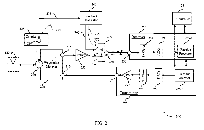
devices, and
apparatuses that support satellite terminal radio frequency loopback.
Generally, the described systems
and techniques enable a transceiver to perform self-testing and adjust signals
to be transmitted to a
target device using a loopback signal from a waveguide diplexer in the
transceiver. The loopback
signal may be a feedback signal that is generated from an RF transmit signal
in the waveguide
diplexer. A frequency-translated version of the loopback signal may be
provided to a receiver in the
transceiver. The receiver may compare the translated loopback signal with a
representation of the
intended transmit signal and generate a compensation signal based on the
comparison. A transmitter
in the transceiver may use the compensation signal to adjust subsequent
signals to be transmitted to
the target device. Thus, the loopback signal may enable the transceiver to
adjust transmissions to
compensate for distortion introduced into the transmit signal from the digital
domain to the RF
domain.
[0005] A transceiver for communicating with a target device is
described. The transceiver may
include a waveguide diplexer having a common port coupled to first and second
individual ports, the
1
CA 03089340 2020-07-22
WO 2019/152793
PCT/US2019/016273
first individual port associated with a transmit frequency range and the
second individual port
associated with a receive frequency range. The transceiver may include a
transmitter coupled with the
first individual port of the waveguide diplexer and configured to output a
transmit signal to the first
individual port within the transmit frequency range. The transceiver may
include a bidirectional
coupler having a coupled port coupled with the common port of the waveguide
diplexer. The
transceiver may include a loopback translator coupled with the coupled port
and configured to obtain
a loopback signal associated with the transmit signal via the coupled port,
and to translate the
loopback signal from within the transmit frequency range to within the receive
frequency range. The
transceiver may include a receiver having in input port coupled with the
second individual port of the
waveguide diplexer and coupled with the loopback translator via a loopback
path, where the receiver
is configured to, in a first mode, obtain a received signal from the target
device via the waveguide
diplexer, and, in a second mode, obtain the translated loopback signal via the
loopback path and
compare the translated loopback signal to a representation of the transmit
signal to generate a
compensation signal, where the transmitter is further configured to receive
the compensation signal
and adjust the transmit signal based at least in part on the compensation
signal.
[0006] A method for compensating transmit signals transmitted to a
target device is described.
The method may include providing a first transmit signal to a first individual
port of a waveguide
diplexer, the waveguide diplexer having a common port coupled to the first
individual port and a
second individual port, the first individual port associated with a transmit
frequency range and the
second individual port associated with a receive frequency range. The method
may include coupling a
loopback signal associated with the first transmit signal from the common port
of the waveguide
diplexer. The method may include translating the loopback signal from within
the transmit frequency
range to within the receive frequency range. The method may include inputting,
to a receiver while in
a first mode, a receive signal from the target device via the waveguide
diplexer, and inputting, to the
receiver while in a second mode, the translated loopback signal via a loopback
path. The method may
include comparing, in the second mode, the translated loopback signal with a
representation of the
first transmit signal and adjusting a second transmit signal based on the
comparison. The method may
include providing the second transmit signal to the first individual port of
the waveguide diplexer for
transmission to the target device.
BRIEF DESCRIPTION OF THE DRAWINGS
[0007] FIG. 1 illustrates an example of an RF communication system that
supports satellite
terminal radio frequency loopback in accordance with aspects of the present
disclosure.
[0008] FIG. 2 illustrates an example of a transceiver that supports
satellite terminal radio
frequency loopback in accordance with aspects of the present disclosure.
2
CA 03089340 2020-07-22
WO 2019/152793
PCT/US2019/016273
[0009] FIG. 3 illustrates an example of a transceiver that supports
satellite terminal radio
frequency loopback in accordance with aspects of the present disclosure.
[0010] FIG. 4 illustrates an example of a loopback translator that
supports satellite terminal radio
frequency loopback in accordance with aspects of the present disclosure.
[0011] FIG. 5 illustrates an example of a waveguide device that supports
satellite terminal radio
frequency loopback in accordance with aspects of the present disclosure.
[0012] FIG. 6 illustrates an example of a waveguide device that supports
satellite terminal radio
frequency loopback in accordance with aspects of the present disclosure.
[0013] FIG. 7 illustrates an example of a method that supports satellite
terminal radio frequency
loopback in accordance with aspects of the present disclosure.
DETAILED DESCRIPTION
[0014] Many communication systems use radio frequency (RF) signals for
communications
between a target device and a terminal. For example, RF signals are used for
communications
between satellites and ground-based or vehicle-based terminals, and for many
other types of
communications.
[0015] A terminal may include a transceiver for transmitting and
receiving RF signals to and
from the target device via an antenna. In some cases, the transceiver may be a
multi-frequency
transceiver that transmits RF signals at frequencies within a first frequency
range and receives RF
signals at frequencies within a second (different) frequency range. For
example, the transceiver may
transmit signals at approximately 30 GHz and may receive signals at
approximately 20 GHz. Using
different frequencies for transmitting and receiving may reduce interference
between transmitted and
received signals and/or allow the transceiver to concurrently transmit and
receive signals.
[0016] In some cases, a multi-frequency transceiver may include a
waveguide diplexer for
frequency-domain multiplexing of RF signals. The waveguide diplexer may serve
as a filter that
separates or combines RF signals based on frequency. The waveguide diplexer
may include three
ports: a first individual port that passes signals within a first frequency
range (e.g., a transmit
frequency range) and rejects signals outside of that range, a second
individual port that passes signals
within a second frequency range (e.g., a receive frequency range) and rejects
signals outside of that
range, and a common port coupled with the first individual port and second
individual port that passes
signals in both frequency ranges. The common port of the waveguide diplexer
may be coupled with
an antenna for transmitting and receiving signals with the target device.
3
CA 03089340 2020-07-22
WO 2019/152793
PCT/US2019/016273
[0017] In some cases, a receive path of a transceiver (e.g., an
electrical path along which signals
may be received from the target device) may include the waveguide diplexer, an
analog-to-digital
converter (ADC) to convert the received signal to the digital domain, and
various other analog and/or
digital components along the way.
[0018] Similarly, a transmit path of a transceiver may include a digital-to-
analog converter
(DAC) to convert a digital transmit signal to an analog transmit signal, a
high-powered amplifier to
amplify the transmit signal, the waveguide diplexer, and various other analog
and/or digital
components along the way.
[0019] In some cases, signals to be transmitted from the terminal to the
target device may be
affected (e.g., distorted) by various characteristics or operating conditions
of the transceiver, such as
by process variations associated with components in the transmit path, noise,
amplitude/phase
distortions, or non-linearities introduced by components in the transmit path,
and/or temperature
variations during operation, for example. Thus, the actual RF signal
transmitted by a transceiver may
differ from the intended transmit signal; e.g., the transmit signal generated
in the digital domain.
[0020] Some transceivers may include a feedback mechanism to compensate for
such distortion
before the signal is transmitted to the target device; e.g., to pre-adjust
transmit signals before they are
provided to the antenna for transmission. In some cases, the feedback
mechanism may include a
feedback signal that is generated in the digital or analog domain of the
transceiver; that is, a feedback
signal may be obtained from a node in the digital or analog portion of the
transmit path and may be
fed back to a processor in the transceiver. The processor may adjust
subsequent transmit signals in the
digital domain based on the feedback. This approach, however, may neglect the
effect of components
that are downstream from the node in the transmit path. Thus, it may be
desirable to provide feedback
from a node that is as close to the antenna as possible.
[0021] In some cases, a transceiver may be calibrated before it is
deployed in the field to
characterize the effects of such variations. The transceiver may be calibrated
by running a calibration
test (e.g., using separate calibration equipment) to characterize these
effects. The resulting calibration
information may be stored in the terminal to enable subsequent adjustment of
signals during
operation. Similarly, a transceiver may perform self-testing before it is
deployed to test various
components in the transceiver. Such one-time calibration tests and self-tests
may not, however,
capture dynamic effects that may arise due to temperature variations during
operation of the
transceiver in the field or due to component aging, for example. Thus, it may
be desirable to enable
self-test and calibration of a transceiver in the field, such as while the
transceiver is deployed and
configured to communicate with a target device. Moreover, it may be desirable
to enable real-time
calibration, self-test, and signal compensation while the transceiver is
actively communicating with a
target device.
4
CA 03089340 2020-07-22
WO 2019/152793
PCT/US2019/016273
[0022] According to various aspects, a loopback translator coupled with
a loopback path to the
receiver may address the dual objectives of providing feedback from a node
that is close to the
antenna and enabling calibration and self-test in the field. For example, a
transceiver may include a
loopback path for providing a loopback signal from the waveguide diplexer to a
receiver. The
loopback signal may be a frequency translated version of the transmit signal
that enables the
transceiver to adjust the transmit signal based on feedback from the RF domain
(e.g., the waveguide
diplexer) rather than from the analog or digital domain. In this case, the
loopback signal may include
the effect of components in the transmit path between the digital domain and
the RF domain, thereby
potentially providing a more accurate feedback mechanism.
[0023] In some cases, the loopback signal may be obtained from the
waveguide diplexer by, for
example, coupling an RF transmit signal from the common port of the waveguide
diplexer to generate
an analog loopback signal. In this case, the loopback signal may be based on
the transmit signal and
may have a frequency within the transmit frequency range.
[0024] The loopback signal may be provided to a loopback translator in
the transceiver. The
loopback translator may translate the loopback signal from within the transmit
frequency range to
within the receive frequency range, thereby generating a translated loopback
signal. In some cases, the
transmit frequency range may include higher frequencies than the receive
frequency range. Returning
to the previous example, the loopback translator may translate, for example, a
coupled version of a 30
GHz transmit signal (e.g., loopback signal) to a 20 GHz translated loopback
signal. The translated
loopback signal may then be provided, via a loopback path, to a receiver in
the transceiver.
[0025] The receiver may be used for receiving signals from the target
device at frequencies
within the receive frequency range and may also be used for receiving the
translated loopback signal
within the receive frequency range. The receiver may be coupled with the
second individual port of
the waveguide diplexer for receiving signals at the receive frequencies from
the waveguide diplexer.
[0026] In some cases, translating the loopback signal from the transmit
frequency range to the
receive frequency range allows the same receiver hardware (e.g., low noise
amplifier (LNA),
downconverter, demodulator) to be used for receiving signals from the target
device (via the
waveguide diplexer) and for receiving the translated loopback signal, thereby
enabling the transceiver
to compensate transmit signals in the field without having separate receiver
circuitry for receiving
signals in the transmit frequency range.
[0027] In some cases, the receiver may compare the translated loopback
signal to a
representation of the transmit signal on which the loopback signal is based,
such as a stored version of
the transmit signal. The receiver may generate a compensation signal based on
the comparison and
5
CA 03089340 2020-07-22
WO 2019/152793
PCT/US2019/016273
may provide the compensation signal to the transmitter to enable the
transmitter to adjust subsequent
transmissions based on the compensation signal.
[0028] As previously noted, the receiver may receive the translated
loopback signal via a
loopback path. In some cases, the loopback path may include a path through the
waveguide diplexer;
that is, the translated loopback signal may be "looped back" from the loopback
translator through the
common port of the waveguide diplexer to the second individual port of the
waveguide diplexer and
provided to the receiver via the second individual port. In this case, the
path from the second
individual port to the receiver may be shared by the loopback path and the
receive path such that the
receiver can receive signals from the target device and receive the translated
loopback signal at
different times using the same path.
[0029] In some cases, a transceiver may include a second loopback path,
such as a direct
connection between the loopback translator and the receiver. In this case, the
translated loopback
signal may be provided to the receiver via the second loopback path without
using the receive path.
[0030] In some cases, a transceiver may include two waveguide diplexers
that may be configured
to pass the same transmit and receive frequency ranges, but may each be
associated with a different
signal polarization, such as a left-hand circular polarization (LHCP) or right-
hand circular polarization
(RHCP). Both waveguide diplexers may be coupled with the same antenna via a
polarizer (e.g.,
septum polarizer), for example. In this case, the transceiver may also include
two receivers, and may
be capable of receiving two signals having substantially the same frequency
(e.g., within the receive
frequency range) but different polarizations. Similarly, the transceiver may
be capable of transmitting
via either LHCP or RHCP (e.g., via different waveguide diplexers).
Additionally or alternatively, the
transceiver may have multiple transmitters, and may be capable of concurrently
transmitting LHCP
and RHCP signals with substantially the same frequency (e.g., within the
transmit frequency range).
The second waveguide diplexer may also be used to generate a loopback signal,
and a receive signal
switch matrix may be used to route the loopback signal and signals received
from the target device to
an available receiver.
[0031] Systems and techniques for radio frequency loopback for
transceivers as described herein
may provide many benefits. For example, transceivers described herein may
enable self-test and
compensation of transmission signals while the transceiver is "on air;" e.g.,
while the transceiver is
deployed in the field and may be actively communicating with a target device.
Thus, transceivers
described herein may be able to compensate transmission signals based on real-
time operating
conditions and maintain calibration over time in the presence of temperature
variations and
component aging. Moreover, transceivers described herein may use the same
receiver hardware for
receiving a loopback signal and for receiving signals from the target device.
Such shared receiver
functionality may reduce the need for additional hardware to compensate
transmission signals. Still
6
CA 03089340 2020-07-22
WO 2019/152793
PCT/US2019/016273
further, the transceivers described herein provide feedback from the RF domain
(e.g., from the
waveguide diplexer), which may capture the effects of more components in the
transmit path than
feedback from the analog or digital domain. This technique may, in turn,
enable the use of lower-cost
components, such as lower-cost power amplifiers, because any additional
distortion introduced by the
lower-cost components may be compensated by the transmitter.
[0032] Aspects of the disclosure are initially described in the context
of an RF communication
system. Aspects of the disclosure are further illustrated by and described
with reference to simplified
transceiver circuits and waveguide diplexers. Aspects of the disclosure are
further illustrated by and
described with reference to apparatus diagrams, system diagrams, and
flowcharts that relate to
satellite terminal radio frequency loopback. Although described with the
example that the transmit
frequency range is higher than the receive frequency range, it should be
understood that the
techniques discussed above for radio frequency loopback may be applied where
the transmit
frequency range is lower than the receive frequency range.
[0033] FIG. 1 illustrates an example of an RF communication system 100.
RF communication
system includes a terminal device 105 that may communicate with a target
device 110 by transmitting
RF transmit signals 125 and receiving RF receive signals 130 via antenna 120
and transceiver 115. In
some cases, antenna 120 may be part of transceiver 115 and/or terminal device
105. In some cases,
terminal device 105 may be a gateway or user terminal device that may be
stationary or may be
located on a vehicle, such as on an airplane or ship. In some cases, target
device 110 may be a
satellite.
[0034] In some cases, RF transmit signals 125 may be transmitted at a
frequency within a
transmit frequency range, and RF receive signals 130 may be received at a
frequency within a
(different) receive frequency range.
[0035] In some cases, transceiver 115 may be configured to adjust
transmit signals to
compensate for distortion introduced in the transmit path by obtaining, from a
waveguide diplexer in
transceiver 115, a loopback signal associated with a transmit signal in the
waveguide diplexer,
translating the loopback signal from the transmit frequency range to the
receive frequency range,
comparing the translated loopback signal with a representation of the transmit
signal, and adjusting
subsequent transmit signals based on the comparison.
[0036] Additional details regarding the circuitry and operation of
transceiver 115 are discussed
with reference to FIGs. 2 through 6.
[0037] FIG. 2 illustrates a simplified example of a transceiver 200 that
supports satellite terminal
radio frequency loopback in accordance with aspects of the present disclosure.
In some examples,
7
CA 03089340 2020-07-22
WO 2019/152793
PCT/US2019/016273
transceiver 200 may be an example of transceiver 115 in RF communication
system 100. In some
cases, transceiver 200 may include additional components that are omitted from
FIG. 2 for clarity.
[0038] Transceiver 200 includes antenna 120-a, which may be used to
receive and transmit RF
signals to and from a target device as depicted in FIG. 1. Antenna 120-a may
include, for example, a
horn antenna or feedhorn, and signals may be directed to antenna 120-a via a
reflector (e.g., parabolic
reflector). In some cases, antenna 120-a may include a phased array.
[0039] Transceiver 200 includes waveguide diplexer 205. Waveguide
diplexer 205 has a first
individual port 210 associated with a transmit frequency range, a second
individual port 215
associated with a receive frequency range different than the transmit
frequency range, and a common
port 220 coupled with the first individual port 210 and the second individual
port 215 and associated
with the transmit frequency range and the receive frequency range.
[0040] The first individual port 210 may be coupled with the common port
via a first waveguide
that is configured to pass signals within the transmit frequency range and may
reject signals outside of
the transmit frequency range. The second individual port 215 may be coupled
with the common port
via a second waveguide that is configured to pass signals within the receive
frequency range and may
reject signals outside of the receive frequency range. The first and second
waveguides may be coupled
with the common port via a junction (e.g., E-plane T-junction, H-plane T-
junction). The common port
220 may be a waveguide that is configured to pass signals within the transmit
frequency range and the
receive frequency range and may reject signals outside of the transmit
frequency range and receive
frequency range.
[0041] The common port 220 may be a waveguide that is coupled with
antenna 120-a to provide
signals to the antenna that are within the transmit frequency range and to
receive signals from antenna
120-a within that are within the receive frequency range. In some cases, the
first individual port may
be used for transmitting signals to the target device (e.g., via common port
220 and antenna 120-a),
the second individual port may be used for receiving signals from the target
device (e.g., via antenna
120-a and common port 220). Thus, the waveguide diplexer may be configured to
enable
bidirectional, multi-frequency RF communications with the target device.
Examples of waveguide
diplexer 205 are further described and depicted with reference to FIGs. 5 and
6.
[0042] Transceiver 200 includes a bidirectional coupler 225 having a
coupled port 230. Coupled
port 230 may be coupled with common port 220 and with conductive connection
235 and may be used
to couple RF signals from the common port onto conductive connection 235,
and/or to couple analog
signals on conductive connection 235 into the common port 220. That is,
coupler 225 may be used to
induce (e.g., generate) an analog signal on conductive connection 235 based on
an RF signal in
8
CA 03089340 2020-07-22
WO 2019/152793
PCT/US2019/016273
common port 220, or to induce an RF signal in common port 220 based on an
analog signal on
conductive connection 235.
[0043] In some cases, coupler 225 may be a passive coupler that
bidirectionally couples signals
between the common port 220 and the conductive connection 235 when signals are
present in the
common port 220 or on the conductive connection 235. In some cases, coupled
port 230 may be or
may include a coupling hole in or on the common port 220 (or a waveguide
coupled with the common
port 220) to enable bidirectional coupling between the common port 220 and the
conductive
connection 235, as depicted in the example of FIG. 5.
[0044] In some cases, coupler 225 may couple a transmit signal from
common port 220 to induce
a loopback signal on conductive connection 235 that is based on the RF
transmit signal in the
common port 220. Because the loopback signal is based on the transmit signal,
the loopback signal
may have a frequency that is within the transmit frequency range.
[0045] Transceiver 200 includes a loopback translator 240. Loopback
translator 240 may be
coupled with the coupled port 230 via conductive connection 235 and may be
configured to obtain the
loopback signal via coupled port 230. Loopback translator 240 may be
configured to translate the
loopback signal from a frequency within the transmit frequency range to a
frequency within the
receive frequency range to generate a translated loopback signal. Loopback
translator 240 may
include various circuitry for performing the frequency translation, as
depicted in the example of FIG.
4.
[0046] Transceiver 200 includes receiver 245. Receiver 245 may be coupled
with second
individual port 215 of waveguide diplexer 205 and may be configured to receive
signals from the
target device via waveguide diplexer 205. Receiver 245 may include a receive
(Rx) chain 283, which
may include various components for amplifying, filtering, downconverting, or
demodulating received
signals or for performing other functionality. Receiver 245 may include one or
more analog-to-digital
converters (ADCs) 290 for converting signals received by receiver 245 from the
analog domain to the
digital domain. Receiver 245 may include receiver processor 285-a for
processing received signals in
the digital domain. Receive processor 285-a may include a microprocessor,
microcontroller, digital
signal processor (DSP), field-programmable gate array (FPGA), application-
specific integrated circuit
(ASIC), and/or other type of processing hardware. Receiver 245 may include
various other
components that are not shown in FIG. 2 for clarity.
[0047] Receiver 245 may also be configured to receive the translated
loopback signal from the
loopback translator 240 via a loopback path, and to compare the translated
loopback signal with a
representation of the transmit signal on which the loopback signal is based
(e.g., the transmit signal
from which the loopback signal was coupled). The representation of the
transmit signal may be, for
9
CA 03089340 2020-07-22
WO 2019/152793
PCT/US2019/016273
example, a digital representation of the transmit signal saved by transceiver
200 for subsequent use by
receiver 245. In some cases, receiver 245 may be configured to generate a
compensation signal based
on the comparison of the translated loopback signal with the representation of
the transmit signal. In
some cases, receiver 245 may compare the translated loopback signal with the
representation of the
transmit signal and generate the compensation signal using receive processor
285-a, for example. The
compensation signal may subsequently be used by a transmitter 295 in
transceiver 200 to compensate
(e.g., adjust) transmit signals.
[0048] In some cases, the loopback path may be or may include loopback
path 250. In this case,
the translated loopback signal from loopback translator 240 is looped back
through the coupled port
230 into the common port 220 and provided to the receiver 245 via the second
individual port 215.
That is, the loopback path 250 may include the common port 220 and second
individual port 215 of
the waveguide diplexer. In this case, receiver 245 may receive signals from
the target device and
receive the translated loopback signal from second individual port 215 at
different times, allowing
transceiver 200 to perform transmit signal compensation using existing
circuitry. However, in this
case, transceiver 200 may not be able to perform signal compensation while
receiver 245 is actively
receiving signals from the target device, because the loopback signal and
receive signals from the
target device would interfere with each other (e.g., second individual port
215 may already be in use).
[0049] In some cases, transceiver 200 may include conductive connection
260 to provide a
second loopback path 255 from loopback translator 240 to receiver 245.
Loopback path 255 may
enable loopback translator 240 to provide a translated loopback signal to
receiver 245 without looping
back through waveguide diplexer 205 and without using second individual port
215.
[0050] In this case, transceiver 200 may include switch 265 to enable
receiver 245 to selectively
receive signals via either loopback path 255 or via second individual port
215. That is, receiver 245
may selectively receive signals received from the target device (via second
individual port 215), or the
translated loopback signal (via conductive connection 260).
[0051] Switch 265 may include a first input port 270 coupled with
conductive connection 260
and a second input port 275 coupled with second individual port 215. Switch
265 may include an
output port 280 coupled with an input port 250 of receiver 245. Switch 265 may
be configured to
select input port 270 or input port 275 for coupling with output port 280.
[0052] For example, if switch 265 selects input port 270, switch 265 may
establish an electrical
connection between conductive connection 260 and receiver 245. Thus, switch
265 may select input
port 270 to provide a translated loopback signal to receiver 245 by
establishing loopback path 255.
[0053] For example, if switch 265 selects input port 275, switch 265 may
establish an electrical
connection between second individual port 215 and receiver 245. Thus, switch
265 may select input
CA 03089340 2020-07-22
WO 2019/152793
PCT/US2019/016273
port 275 to provide a signal received from the target device to receiver 245,
or to provide the
translated loopback signal to receiver 245 by establishing loopback path 250.
[0054] In some cases, transceiver 200 may include LNA 252 between the
second individual port
215 and the receiver 245 for amplifying a signal received from the target
device or the translated
loopback signal (e.g., prior to switch 265 or Rx chain 283).
[0055] In some cases, transceiver 200 (or portions of transceiver 200,
such as switch 265,
receiver 245, coupler 225, and/or loopback translator 240) may be configured
to operate in either a
first mode associated with receiving signals from the target device or in a
second mode associated
with receiving the translated loopback signal to perform transmit signal
compensation. For example,
in some cases, transceiver 200 may include a controller 281 that may configure
transceiver 200 (or
portions of transceiver 200, such as switch 265, receiver 245, coupler 225,
and/or loopback translator
240) to operate in the first mode or the second mode by providing various
control signals to switch
265, receiver 245, coupler 225, loopback translator 240, and/or to other
components in transceiver
200 to cause transceiver 200 to operate in the first mode or the second mode.
[0056] Thus, receiver 245 may be configured to, in the first mode, receive
a signal received from
the target device, and to, in the second mode, receive the translated loopback
signal from the loopback
translator 240 (e.g., via loopback path 250 or loopback path 255). For
example, loopback translator
240 may be configured to, in the second mode, input the translated loopback
signal to the common
port 220 of the waveguide diplexer 205 via coupler 225. Alternatively, when
present, switch 265 may
be configured to output to receiver 245, in the first mode, a signal received
from the target device
(e.g., by selecting input port 275), and to output to the receiver, in the
second mode, the translated
loopback signal (e.g., by selecting port 270 to select loopback path 255, or
by selecting input port 275
to select loopback path 250.
[0057] In some cases, receiver 245 may be configured to, in the second
mode, obtain the
.. translated loopback signal and/or compare the translated loopback signal
with the representation of
the transmit signal upon which the loopback signal is based. Receiver 245 may
be configured to
generate a compensation signal based on the comparison of the translated
loopback signal with the
representation of the transmit signal.
[0058] In some cases, receiver 245 may be configured to enter the second
mode periodically to
receive the translated loopback signal from the loopback translator. That is,
receiver 245 may be
configured to receive the loopback signal periodically, at predetermined time
intervals, such as for
periodic self-test or calibration. In some cases, transceiver 200 may store
calibration values associated
with the self-test or calibration, which may subsequently be used to adjust
transmit signals or for
diagnostic purposes.
11
CA 03089340 2020-07-22
WO 2019/152793
PCT/US2019/016273
[0059] In some cases, receiver 245 may be configured to enter the second
mode based on the
scheduling of downlink communications from the target device (e.g.,
availability of receiver 245 to
receive a translated loopback signal). For example, receiver 245 may be
configured to enter the
second mode at times when receiver 245 is not receiving a signal from the
target device and therefore
may be able to obtain the translated loopback signal via loopback path 250.
[0060] In some cases, receiver 245 may be configured to enter the second
mode in response to
receiving a command or a trigger. For example, receiver 245 may receive a
command from, e.g.,
processor 285-a or 285-b or another source specifying that receiver 245 should
perform a self-test or
calibration routine, and receiver 245 may respond to receiving the command by
entering the second
mode to obtain the translated loopback signal, compare the translated loopback
signal with the
representation of the transmit signal, and generate a compensation signal.
Additionally or
alternatively, a trigger indicating that receiver 245 should enter the second
mode may be identified in
response to detecting a change in transceiver operating conditions, such as a
change in temperature,
location, time of day, or other operating condition. In some cases, receiver
245 may be configured to
enter the second mode based on a trigger and receiver availability (e.g.,
entering the second mode at a
next available time period after a trigger).
[0061] In some cases, receiver 245 may compare the translated loopback
signal with the
representation of the transmit signal by comparing, for example, the
frequency, phase, polarity, and/or
power of the two signals. In some cases, the compensation signal may be based
on the comparison,
and may include an indication of the difference in frequency, phase, polarity,
and/or power of the two
signals, such as an indication of an amount of the difference(s), a sign of
the difference(s) (e.g.,
positive or negative), etc. In some cases, the compensation signal may include
an indication of an
amount by which to adjust transmit signals, such as an amount of frequency,
phase, or power.
[0062] In some cases, the compensation signal may be provided to
transmitter 295 to enable
transmitter 295 to adjust transmit signals based on the compensation signal.
[0063] Transmitter 295 may be coupled with receiver 245 and with first
individual port 210 of
waveguide diplexer 205. Transmitter 295 may be configured to output transmit
signals (e.g., signals to
be transmitted to a target device) via output port 251 to first individual
port 210. Transmitter 295 may
be configured to output the transmit signals at a frequency within the
transmit frequency range, for
example.
[0064] Transmitter 295 may include transmit processor 285-b for
adjusting transmit signals
based on the compensation signal. Transmit processor 285-b may include a
microprocessor,
microcontroller, DSP, FPGA, ASIC, and/or other type of processing hardware. In
some cases,
transmit processor 285-b may be coupled with receive processor 285-a. In some
cases, transmit
12
CA 03089340 2020-07-22
WO 2019/152793
PCT/US2019/016273
processor 285-b may share some or all of its processing hardware with receive
processor 285-a. In
some cases, transmit processor 285-b may be the same processor as receive
processor 285-a.
[0065] Transmitter 295 may include one or more digital-to-analog
converters (DACs) 292 for
converting digital signals to analog signals. Transmitter 295 may include a
transmit chain 293, which
.. may include various components for upconverting and/or modulating signals
to be transmitted or for
performing other functionality.
[0066] In some cases, transmitter 295 may include a power amplifier (PA)
297 for amplifying
the adjusted transmit signal; e.g., for amplifying the power of the transmit
signal after transmitter 295
has adjusted the transmit signal. Power amplifier 297 may be coupled (e.g.,
via output port 251) with
the first individual port 210 of waveguide diplexer 205. Transmitter 295 may
include various other
components that are not shown in FIG. 2 for clarity.
[0067] Transmitter 295 may be configured to adjust transmit signals in a
variety of manners,
based on the compensation signal. For example, transmitter 295 may be
configured to adjust transmit
signals by adjusting the frequency, phase, or polarity of the transmit signals
to compensate for
distortion introduced in the transmit path as identified by comparing the
translated loopback signal
and the transmit signal.
[0068] In some cases, the transmit signal may be modulated using, for
example, quadrature
amplitude modulation (QAM) or another modulation scheme. In this case, the
signal may be
transmitted by transmitting symbols (e.g., QAM symbols) at a particular symbol
rate, where the
symbol rate is the number of symbols transmitted per unit time. In some cases,
transmitter 295 may be
configured to adjust transmit signals by adjusting the symbol rate of the
transmit signals based on the
compensation signal. For example, the transmitter 295 may increase or decrease
the symbol rate of the
transmit signals depending on the amount of distortion introduced into the
transmit signal.
[0069] In some cases, transmitter 295 may be configured to adjust
transmit signals by adjusting
the slew rate of the transmit signals based on the compensation signal. The
slew rate may be the rate
at which a signal transitions from a high voltage to a low voltage (or vice
versa); that is, the slew rate
may represent the slope of the transition between high and low voltages.
[0070] In some cases, transmitter 295 may be configured to adjust
transmit signals by adjusting a
frequency-dependent gain slope, a frequency-dependent phase variation, a time-
dependent transient
amplitude, a time-dependent transient phase, a frequency and amplitude
dependent amplitude
modulation, and/or a frequency and amplitude dependent phase modulation.
[0071] In some cases, transmitter 295 may be configured to adjust
transmit signals by adjusting
the transmit power of the transmit signals based on the compensation signal.
13
CA 03089340 2020-07-22
WO 2019/152793
PCT/US2019/016273
[0072] FIG. 3 illustrates a simplified example of a transceiver 300 that
supports satellite terminal
radio frequency loopback in accordance with aspects of the present disclosure.
In some examples,
transceiver 300 may be an example of transceiver 115 in RF communication
system 100. In some
cases, transceiver 300 may include additional components that are omitted from
FIG. 3 for clarity.
[0073] Transceiver 300 may depict an example of a transceiver that includes
two waveguide
diplexers and two receivers to enable transceiver 300 to concurrently receive,
using the two receivers,
two signals from a target device and/or to concurrently receive a signal from
a target device and a
translated loopback signal from a loopback translator.
[0074] Transceiver 300 includes antenna 120-b, which may be used to
receive and transmit RF
.. signals to and from a target device as depicted in FIG. 1. Antenna 120-b
may include, for example, a
horn antenna or feedhorn, and signals may be directed to antenna 120-b via a
reflector (e.g., parabolic
reflector).
[0075] Transceiver 300 includes two waveguide diplexers 205-a, 205-b.
Waveguide diplexers
205-a, 205-b may be examples of waveguide diplexer 205 described with
reference to FIG. 2 and may
operate in a similar manner. Each waveguide diplexer 205-a, 205-b has a first
individual port 210-a,
210-b associated with a transmit frequency range, a second individual port 215-
a, 215-b associated
with a receive frequency range different than the transmit frequency range,
and a common port 220-a,
220-b coupled with the first individual port 210-a, 210-b and the second
individual port 215-a, 215-b
and associated with the transmit frequency range and the receive frequency
range.
[0076] Transceiver 300 includes polarizer 310 for dividing or combining
signals based on their
polarization (e.g., RHCP, LHCP, linear polarizations). Polarizer 310 may
enable a single antenna 120-
b to be used with the two waveguide diplexers 205-a, 205-b by dividing
received waves based on their
polarization and by combining signals having different polarizations for
transmission.
[0077] Polarizer 310 may be coupled with both waveguide diplexers 205-a,
205-b. Polarizer 310
.. may receive RF signals from a target device having a first and/or second
polarization and may route
signals of the first polarization (e.g., RHCP, first linear polarization) to
waveguide diplexer 205-a and
route signals of the second polarization (e.g., LHCP, second linear
polarization) to waveguide
diplexer 205-b, for example. Similarly, polarizer 310 may receive signals from
waveguide diplexer
205-a and may polarize signals from waveguide diplexer 205-a to have the first
polarization for
transmission to the target device. Polarizer 310 may receive signals from
waveguide diplexer 205-b
and may polarize signals from waveguide diplexer 205-b to have the second
polarization for
transmission to the target device. In some cases, polarizer 310 may be a
septum polarizer that may
transfer energy of a received signal corresponding to different orthogonal
basis polarizations (e.g.,
RHCP, LHCP) to different divided waveguides and convert component signals
travelling from the
14
CA 03089340 2020-07-22
WO 2019/152793
PCT/US2019/016273
different divided waveguides to the orthogonal basis polarizations in a
combined polarization signal,
for example.
[0078] Transceiver 300 includes bidirectional couplers 225-a, 225-b,
each of which has a
coupled port 230-a, 230-b. Couplers 225-a, 225-b may each be an example of a
coupler 225 described
with reference to FIG. 2.
[0079] Each coupled port 230-a, 230-b may be coupled with a common port
220-a, 220-b of a
waveguide diplexer 205-a, 205-b and with a conductive connection 235-a, 235-b
and may be used to
couple RF signals from the respective common port 220-a, 220-b onto the
conductive connection 235-
a, 235-b, and/or to couple analog signals on conductive connection 235-a, 235-
b into an RF signal in
the respective common port 220-a, 220-b. That is, couplers 225-a, 225-b may
each be used to induce
(e.g., generate) an analog signal on a respective conductive connection 235-a,
235-b based on an RF
signal in common port 220-a, 220-b, or to induce an RF signal in common port
220-a, 220-b based on
an analog signal on conductive connection 235-a, 235-b.
[0080] In some cases, each coupler 225-a, 225-b may be configured to
couple a transmit signal
from common port 220-a, 220-b to induce a loopback signal on conductive
connection 235-a, 235-b
that is based on an RF transmit signal in the common port 220-a, 220-b. Thus,
transceiver 300 may
support loopback signals from either waveguide diplexer 205-a, 205-b.
[0081] Transceiver 300 includes loopback translator 240-a. Loopback
translator 240-a may be an
example of loopback translator 240 described with reference to FIG. 2.
Loopback translator 240-a
may be coupled with each coupled port 230-a, 230-b via respective conductive
connection 235-a, 235-
b and may be configured to obtain the loopback signal via either coupled port
230-a, 230-b. Loopback
translator 240-a may be configured to translate the loopback signal from a
frequency within the
transmit frequency range to a frequency within the receive frequency range to
generate a translated
loopback signal.
[0082] Transceiver 300 includes two receivers 245-a, 245-b for receiving
signals within the
receive frequency range, and transceiver 300 includes a receive signal switch
matrix 315 for routing
the signals to the receivers 245-a, 245-b. In some cases, receive signal
switch matrix 315 may enable
either receiver 245-a or 245-b to receive signals from either waveguide
diplexer 205-a or 205-b. Such
signals may be signals received from a target device and/or translated
loopback signals received from
a loopback translator 240-a by looping the translated loopback signal back
through one of the
waveguide diplexers 205-a, 205-b.That is, receive signal switch matrix may be
configured to input, to
one receiver 245-a, a signal received from the target device while inputting,
to the other receiver 245-
b, a translated loopback signal.
CA 03089340 2020-07-22
WO 2019/152793
PCT/US2019/016273
[0083] In some cases, transceiver 300 (or portions of transceiver 300,
such as some or all of
receive signal switch matrix 315, receiver 245-a, 245-b, coupler 225-a, 225-b,
and/or loopback
translator 240-a) may be configured to operate in either a first mode
associated with receiving signals
from a target device or in a second mode associated with receiving a
translated loopback signal to
perform transmit signal compensation, as described with reference to FIG. 2.
[0084] For example, one of receivers 245-a, 245-b may be configured to,
in the second mode,
receive a translated loopback signal, compare the translated loopback signal
with a representation of
the transmit signal from which the loopback signal was coupled, and generate a
compensation signal.
In some cases, in the second mode, one receiver 245 may receive signals from a
target device while
the other receiver 245 receives and compares the translated loopback signal.
[0085] In some cases, the compensation signal may be provided to a
transmitter 295-a in
transceiver 200 to enable transmitter 295-a to adjust transmit signals based
on the compensation
signal, as described with reference to FIG. 2. Transmitter 295-a may be
coupled with first individual
ports 210-a, 210-b of waveguide diplexers 205-a, 205-b via switch 265-c and
may be configured to
output transmit signals (e.g., signals to be transmitted to a target device)
to first individual ports 210-
a, 210-b. Transmitter 295-a may be configured to output the transmit signals
at a frequency within the
transmit frequency range, for example. As discussed with reference to FIG. 2,
transmitter 295-a may
be configured to adjust transmit signals in a variety of manners, based on the
compensation signal.
[0086] Receive signal switch matrix 315 includes two splitters 305-a,
305-b and two switches
265-a, 265-b. Each splitter 305-a, 305-b has an input port 320-a, 320-b that
is coupled with a second
individual port 215-a, 215-b of a waveguide diplexer 205-a, 205-b. In some
cases, input ports 320-a,
320-b may be input ports of the receive signal switch matrix 315, for example.
[0087] Each splitter 305-a, 305-b may be configured to route separate
instances of (e.g., split) a
signal received via a waveguide diplexer 205-a, 205-b to receivers 245-a, 245-
b via various input
ports 275 of switches 265-a, 265-b.
[0088] Each switch 265-a, 265-b has an output port 280-a, 280-b coupled
with a receiver 245-a,
245-b. In some cases, output ports 280-a, 280-b may be output ports of the
receive signal switch
matrix 315, for example. Each switch 265-a, 265-b may be configured to
selectively provide signals
to the corresponding receiver 245-a, 245-b by selecting an input port 275 to
couple the selected input
port 275 with the output port 280 of the switch 265.
[0089] Switch 265-a may include input port 270-a for receiving a
translated loopback signal
from loopback translator 240-a via conductive connection 260-a. Thus, switch
265-a may enable
receiver 245-a to selectively receive a loopback signal via a direct loopback
path, in a manner similar
to that described for loopback path 255 in FIG. 2.
16
CA 03089340 2020-07-22
WO 2019/152793
PCT/US2019/016273
[0090] In transceiver 300, there may be multiple loopback paths between
loopback translator
240-a and receivers 245-a, 245-b. For example, a translated loopback signal
may be looped back, via
conductive connection 235-a or 235-b, through either waveguide diplexer 205-a
or waveguide
diplexer 205-b (e.g., by coupling the translated loopback signal back into the
common port 220-a,
220-b via coupled port 230-a, 230-b). The translated loopback signal may then
be provided to receiver
245-a or receiver 245-b via second individual port 215-a, 215-b and receive
signal switch matrix 315.
As previously noted, transceiver 300 may also include a direct loopback path
from loopback translator
240-a to receiver 245-a via switch 265-a.
[0091] Receivers 245-a, 245-b may be configured to receive a translated
loopback signal from
the loopback translator 240-a via a loopback path, and to compare the
translated loopback signal with
a representation of the transmit signal on which the loopback signal is based
(e.g., the transmit signal
from which the loopback signal was coupled). The inclusion of two waveguide
diplexers 205-a, 205-b
and two receivers 245-a, 245-b may provide transceiver 300 with additional
flexibility for routing
signals received from the target device and for routing loopback signals,
thereby providing more
flexibility for transceiver 300 to perform self-test, calibration, and
transmission signal adjustment
while transceiver 300 is communicating with a target device. For example,
transceiver 300 may be
able to use one receiver 245-a to perform signal compensation while the other
receiver 245-b is
actively receiving signals from a target device.
[0092] Although not shown in FIG. 3 for clarity, in some cases,
transceiver 300 may include
LNAs between the second individual ports 215-a, 215-b and the receivers 245-a,
245-b for amplifying
a signal received from the target device or the translated loopback signal,
such as depicted in FIG. 2.
In some cases, transmitter 295-a may include a power amplifier as depicted in
FIG. 2. In some cases,
receivers 245-a, 245-b may be coupled with a processor in transceiver 300 in a
manner similar to that
shown in FIG. 2 and may be configured to compare the translated loopback
signal with the
representation of the transmit signal and generate the compensation signal via
the processor; e.g., by
providing the translated loopback signal to the processor.
[0093] FIG. 4 illustrates an example of a loopback translator 400 that
supports satellite terminal
radio frequency loopback in accordance with aspects of the present disclosure.
In some examples,
loopback translator 400 may be an example of loopback translator 240, 240-a as
depicted in FIGs. 2
and 3. Loopback translator 400 may include various additional components that
are not shown in FIG.
4 for simplicity. Moreover, other implementations of a loopback translator may
also be used within a
transceiver, such as transceiver 200, 300, without departing from the scope of
the present disclosure.
[0094] Loopback translator 400 includes conductive connection 235-c that
may be used for
receiving a loopback signal from a waveguide diplexer, such as waveguide
diplexer 205, 205-a,
17
CA 03089340 2020-07-22
WO 2019/152793
PCT/US2019/016273
and/or for providing a translated loopback signal to the waveguide diplexer.
Conductive connection
235-c may be an example of conductive connection 235, 235-a as depicted in
FIGs. 2 and 3.
[0095] Loopback translator 400 may include combiner/divider 405-a.
Combiner/divider 405-a
may be coupled with conductive connection 235-c and configured to couple to
conductive connection
235-c to filter 415-a and filter 415-b (potentially via switches 410 and 435,
as described in more detail
below). Combiner/divider 405-a may be configured to split an input signal into
two output signals
and/or to combine two input signals into a single output signal.
[0096] Filter 415-a may be configured to filter a loopback signal
received via, for example,
conductive connection 235-c. In some cases, filter 415-a may be associated
with the transmit
frequency range. For example, in some cases, the loopback signal may have a
frequency within the
transmit frequency range, and filter 415-a may be or include a band pass
filter that may filter the
loopback signal based on a pass band that is roughly centered on a center
frequency of the transmit
frequency range. In some cases, filter 415-a may be or include a high pass
filter that may filter the
loopback signal by passing signals having frequencies that are above a cutoff
frequency, where the
transmit frequency range is above the cutoff frequency.
[0097] Loopback translator 400 includes RF loopback attenuator 420. RF
loopback attenuator
420 may be configured to attenuate (e.g., decrease) a power associated with
the loopback signal
before the loopback signal is translated to a frequency within the receive
frequency range.
[0098] Loopback translator 400 includes local oscillator 425 and mixer
430 for translating the
loopback signal from a frequency within the transmit frequency range to a
frequency within the
receive frequency range to prepare the loopback signal for reception by a
receiver, such as receiver
245. Local oscillator 425 may generate a sinusoidal oscillator signal. Mixer
430 may be coupled with
RF loopback attenuator 420 and local oscillator 425, and may be configured to
generate, based on the
oscillator signal and the loopback signal, a translated loopback signal having
a frequency that is
within the receive frequency range. In some cases, the local oscillator 425
may provide an oscillator
signal having a frequency representing the difference between a center
frequency of the transmit
signals and the center frequency of the receive signals. Where the transmit
frequency is greater than
the receive frequency, the mixer 430 may be used to downconvert the loopback
signal at the transmit
frequency to the translated loopback signal within the receive frequency
range. Where the transmit
frequency is lower than the receive frequency, the mixer 430 may be used to
upconvert the loopback
signal at the transmit frequency to the translated loopback signal within the
receive frequency range.
[0099] Loopback translator 400 includes filter 415-b coupled with mixer
430. Filter 415-b may
be configured to filter the signal received from mixer 430 to pass the
translated loopback signal. Filter
415-b may be associated with the receive frequency range. In some cases,
filter 415-b may include a
18
CA 03089340 2020-07-22
WO 2019/152793
PCT/US2019/016273
band pass filter to filter signals based on a pass band that is roughly
centered on a center frequency of
the receive frequency range. In some cases, filter 415-b may include a low
pass filter that may filter
signals by passing signals that are below a cutoff frequency, where the
receive frequency range is
below the cutoff frequency. In some cases, filter 415-b is configured to
output the translated loopback
signal.
[0100] Filter 415-b may be coupled with conductive connection 235-c
(e.g., via combiner/divider
405-a and/or switch 435) to provide the translated loopback signal to a
receiver. That is, in some
cases, a loopback signal received from a waveguide diplexer may traverse a
frequency translation path
440 in loopback translator 400 that includes filter 415-a, RF loopback
attenuation 420, mixer 430, and
filter 415-b to generate and output the translated loopback signal as an
output of filter 415-b. The
translated loopback signal may then be provided to a receiver, such as
receiver 245-a, 245-b described
with reference to FIGs. 2 and 3.
[0101] In some cases, loopback translator 400 may include conductive
connection 260-b, which
may be configured to provide a translated loopback signal to a receiver
without looping back through
a waveguide diplexer. Conductive connection 260-b may be an example of
conductive connections
260, 260-a described with reference to FIGs. 2 and 3.
[0102] In some cases, if loopback translator includes conductive
connection 260-b, loopback
translator may include switch 435 to select a loopback path by which to
provide the translated
loopback signal to a receiver. That is, switch 435 may select a loopback path
that loops back through
a waveguide diplexer (e.g., via combiner/divider 405-a and conducive
connection 235-c) by selecting
a first output or may select a loopback path that provides the translated
loopback signal directly to the
receiver (e.g., via conductive connection 260-b) by selecting a second output.
[0103] For transceivers that include two waveguide diplexers such as
transceiver 300 of FIG. 3,
loopback translator 400 may include additional circuitry (e.g., conductive
connection 235-d,
combiner/divider 405-b, switch 410, and/or switch 435) to enable loopback
translator 400 to
communicate loopback signals and translated loopback signals with two
waveguide diplexers and two
receivers, for example. In this case, loopback translator 400 may depict an
example of a loopback
translator that may be used in a transceiver having two waveguide diplexers,
such as transceiver 300
depicted in FIG. 3.
[0104] For example, conductive connection 235-d may be used for receiving a
loopback signal
from a second waveguide diplexer, such as waveguide diplexer 205-b, and/or for
providing a
translated loopback signal to the second waveguide diplexer. Conductive
connection may be an
example of conductive connection 235-b described with reference to FIG. 3.
19
CA 03089340 2020-07-22
WO 2019/152793
PCT/US2019/016273
[0105] Combiner/divider 405-b may be coupled with conductive connection
235-d and may be
configured to couple conductive connection 235-d to switch 410 and switch 435.
Combiner/divider
405-b may be configured to split an input signal into two output signals
and/or to combine two input
signals into a single output signal.
[0106] Switch 410 may be coupled with conductive connections 235-c, 235-d
(e.g., via
combiner/dividers 405-a and/or 405-b). Switch 410 may also be coupled with
filter 415-a and may be
configured to route a loopback signal received via either conductive
connection 235-c (e.g., received
from a first waveguide diplexer) or conductive connection 235-d (e.g.,
received from a second
waveguide diplexer) to filter 415-a.
[0107] Similarly, switch 435 may be coupled with conductive connections 235-
c, 235-d (e.g., via
combiner/dividers 405-a, 405-b) and with conductive connection 260-b, if
present. Switch 435 may
also be coupled with filter 415-b and may be configured to route a translated
loopback signal to
conductive connection 260-b, to conductive connection 235-c (e.g., to a first
waveguide diplexer) or
to conductive connection 260-c (e.g., to a second waveguide diplexer).
[0108] Thus, loopback translator 400 may, in some cases, be configured to
receive loopback
signals from either of two waveguide diplexers, route a received loopback
signal through a frequency
translation path 440 to translate the loopback signal to a translated loopback
signal, and route the
translated loopback signal to either of two receivers by routing the
translated loopback signal back
through either of the two waveguide diplexers or directly to a receiver.
[0109] In some cases, the inclusion of switch 410 and switch 435 may enable
a transceiver 300
(e.g., a controller in transceiver 300) to select a coupler 225-a or coupler
225-b for the loopback path
based on various optimization and scheduling criteria. Such criteria may
include, for example,
whether a waveguide diplexer 205-a, 205-b associated with a coupler 225-a, 225-
b is currently
receiving a signal from the target device, whether providing the translated
loopback signal to coupler
225-a, 225-b is likely to cause interference with other signals at waveguide
diplexer 205-a, 205-b, etc.
[0110] FIG. 5 illustrates an example of a waveguide device 500 that
supports satellite terminal
radio frequency loopback in accordance with aspects of the present disclosure.
[0111] Waveguide device 500 includes waveguide diplexer 205-c, which may
be an example of
waveguide diplexer 205, 205-a, 205-b described with reference to FIGs. 2 and
3. Waveguide diplexer
205-c may be designed to pass certain frequencies of an RF signal and reject
other frequencies. That
is, in some cases, the waveguides coupled with the ports of waveguide diplexer
205 may be
configured to act as filters for RF signals, as shown in FIG. 5.
CA 03089340 2020-07-22
WO 2019/152793
PCT/US2019/016273
[0112] Waveguide diplexer 205-c includes first individual port 210-c,
which may be associated
with communicating (e.g., transmitting) signals in the transmit frequency
range. For example,
waveguide diplexer 205-c may include Tx filter 535, which may be a highpass,
lowpass, or bandpass
filter. Waveguide diplexer includes second individual port 215-c, which may be
associated with
communicating (e.g., receiving) signals in the receive frequency range. For
example, waveguide
diplexer 205-c may include Rx filter 525, which may be a highpass, lowpass, or
bandpass filter.
Where the transmit frequency range is higher than the receive frequency range,
for example, the Tx
filter 535 may be a highpass or bandpass filter, and the Rx filter 525 may be
a lowpass or bandpass
filter. Waveguide diplexer includes common port 220-c, which may be associated
with
communicating signals in both the transmit frequency range and receive
frequency range. Common
port 220-c may be coupled with first individual port 210-c and with second
individual port 215-c (e.g.,
via a waveguide junction). Common port 220-c may be coupled with an antenna.
[0113] Waveguide device 500 includes coupled port 230-c, which may be an
example of coupled
port 230, 230-a, or 230-b described with reference to FIGs. 2 and 3. Waveguide
device includes
coupling hole 505, which may be a hole in a waveguide associated with common
port 220-c. Coupled
port 230-c and coupling hole 505 may be included in or may be an example of a
bidirectional coupler,
such as coupler 225, 225-a, 225-b described with reference to FIGs. 2 and 3.
[0114] Coupling hole 505 may be used to couple signals between common
port 220-c and a
conductive connection (e.g., conductive connection 235) that is coupled with
coupling hole 505 via
coupled port 230-c. In some cases, coupling hole 505 may couple signals by
coupling power or
energy between the conductive connection and the common port 220-c.
[0115] In some cases, coupling hole 505 may be used to couple a loopback
signal onto a
conductive connection from a transmit signal in common port 220-c, such as to
provide a loopback
signal to a loopback translator. In some cases, coupling hole 505 may be used
to couple a translated
loopback signal from the conductive connection into the common port 220-c,
such as to provide the
translated loopback signal to a receiver via the loopback path 250 of FIG. 2,
for example.
[0116] In some cases, coupling hole 505 may be configured to provide a
particular coupling
value, which may represent a percentage of energy or power that is coupled. In
some cases, it may be
desirable to design coupling hole 505 such that the coupling value is low
enough not to disturb
transmit signals in common port 220-c but high enough to provide a
sufficiently strong loopback
signal, for example. In some cases, the size or location of coupling hole 505
may be selected to
provide low enough coupling (e.g., a low coupling value) to avoid disturbing
transmit signals while
providing high enough coupling to reduce the variability of the coupled
signal.
21
CA 03089340 2020-07-22
WO 2019/152793
PCT/US2019/016273
[0117] For example, in some cases, the size of coupling hole 505 may be
configured such that
coupling hole 505 has a cutoff frequency above the transmit or receive
frequency ranges and therefore
couples evanescent mode energy without coupling propagating mode energy. For
example, coupling
hole 505 may be a circular hole that is small enough to have a cutoff
frequency higher than signals in
common port 220-c. This technique may reduce the impact of the coupler on
transmit signals, for
example.
[0118] In some cases, coupling hole 505 may be located in an E-plane
wall of common port 220-
c. An E-plane may be a plane associated with an electric field vector, for
example, which may be
orthogonal to an H-plane that is a plane associated with a magnetic field
vector. In general, the center
of an E-plane wall may have little to no current, and therefore the coupling
hole 505 may be offset
from the center of the E-plane wall to provide better coupling, and a
position, size, and cross-sectional
shape of the coupling hole 505 may be selected to provide a desired amount of
coupling.
[0119] In some cases, coupled port 230-c may be part of waveguide
diplexer 205-c or may be a
separate device. For example, common port 220-c may be coupled with an
additional waveguide for
transmitting and receiving signals, and coupled port 230-c may be coupled with
the additional
waveguide.
[0120] FIG. 6 illustrates an example of a waveguide device 600 that
supports satellite terminal
radio frequency loopback in accordance with aspects of the present disclosure.
In some examples,
waveguide device 600 may implement aspects of waveguide diplexer 205, 205-a,
205-b and coupler
225, 225-a, 225-b as depicted in FIGs. 2 and 3.
[0121] Waveguide device 600 includes waveguide diplexer 205-d having a
first individual port
210-d, second individual port 215-d, and common port 220-d. Waveguide diplexer
205-d may be an
example of waveguide diplexer 205-c as described with reference to FIG. 5, for
example. Waveguide
device 600 includes microstrip 605, which may be a conductive element that
spans coupling hole 505.
Microstrip 605 may be separated from the coupling hole 505 by a dielectric
layer, for example.
Microstrip 605 may be part of a coupler, such as coupler 225, and may be used
to conduct (e.g.,
couple) RF energy onto a conductive connection, such as conductive connection
235, 235-a, 235-b
described with reference to FIGs. 2 and 3. Microstrip 605 may be a shielded
microstrip, for example
covered by a housing (not shown) shielding the top of microstrip 605.
Microstrip 605 may also
include one or more impedance matching stubs (not shown), which may be located
on one or both
sides of coupling hole 505.
[0122] FIG. 7 illustrates an example of a method 700 that supports
satellite terminal radio
frequency loopback in accordance with aspects of the present disclosure. In
some examples, method
700 may implement aspects of RF communication system 100.
22
CA 03089340 2020-07-22
WO 2019/152793
PCT/US2019/016273
[0123] Block 705 may include providing a first transmit signal to a
first individual port of a
waveguide diplexer, such as first individual port 210, 210-a, 210-b of
waveguide diplexer 205, 205-a,
205-b, for example. The waveguide diplexer may include a common port coupled
to the first
individual port and a second individual port, such as common port 220, 220-a,
220-b, for example,
which is coupled with first individual port 210, 210-a, 210-b and second
individual port 215, 215-b,
215-c, respectively. The first individual port may be associated with a
transmit frequency range and
the second individual port may be associated with a receive frequency range.
The first transmit signal
may be within the transmit frequency range, for example.
[0124] Block 710 may include coupling a loopback signal associated with
the first transmit
signal from the common port of the waveguide diplexer. In some cases, the
loopback signal may be
coupled from the common port of the waveguide diplexer using a bidirectional
coupler, such as
coupler 225, 225-a, 225-b, for example.
[0125] Block 715 may include translating the loopback signal from within
the transmit frequency
range to within the receive frequency range. In some cases, the loopback
signal is translated from
within the transmit frequency range to within the receive frequency range by a
loopback translator,
such as loopback translator 240, 240-a, 240-b, for example.
[0126] Block 720 may include inputting, to a receiver while in a first
mode, a receive signal from
the target device via the waveguide diplexer. In some cases, the receive
signal may be input to the
receiver via the second individual port of the waveguide diplexer and/or via a
switch, such as switch
265, 265-a, that is coupled with the second individual port of the waveguide
diplexer. In some cases,
[0127] Block 725 may include inputting, to the receiver while in a
second mode, the translated
loopback signal via a loopback path. In some cases, the translated loopback
signal may be input to the
receiver via a loopback path that may include the common port and second
individual port of the
waveguide diplexer or may include a conductive connection such as conductive
connection 260. In
some cases, the translated loopback signal may be input to the receiving via a
switch, such as switch
265, that is coupled with the second individual port of the waveguide diplexer
and/or with the
conductive connection. In some cases, the switch may be configured to, in the
second mode, establish
a loopback path (e.g., loopback path 250, 255, or another loopback path) to
output the translated
loopback signal to the receiver. In some cases, the loopback path may include
a common port and
second individual port of a waveguide diplexer. In some cases, the receive
signal is input to the
receiver during a first time interval and the translated loopback signal is
input to the receiver during a
second time interval.
[0128] Block 730 may include comparing, in the second mode, the
translated loopback signal
with a representation of the first transmit signal. In some cases, the
receiver may compare the
23
CA 03089340 2020-07-22
WO 2019/152793
PCT/US2019/016273
translated loopback signal with a representation of the first transmit signal
using a receive processor,
such as receive processor 285-a, for example. In some cases, the
representation of the first transmit
signal may be a digital representation that is stored by receive processor 285-
a or by a transmit
processor, such as transmit processor 285-b, for example.
[0129] Block 735 may include adjusting a second transmit signal based at
least in part on the
comparison. The second transmit signal may be, for example, a signal that is
transmitted (or is
scheduled to be transmitted) to a target device after the loopback signal has
been coupled from a
previous transmit signal. That is, the loopback signal from the first transmit
signal may be used to
adjust a subsequent transmit signal. In some cases, a transmitter, such as
transmitter 295, 295-a, may
adjust the second transmit signal by adjusting a frequency, a phase, a
polarity, a symbol rate, a slew
rate, a frequency-dependent gain slope, a frequency-dependent phase variation,
a time-dependent
transient amplitude, a time-dependent transient phase, a frequency and
amplitude dependent
amplitude-modulation, a frequency and amplitude dependent phase modulation, or
a transmit power
of the transmit signals. In some cases, a transmitter may be configured to
adjust the second transmit
signal using a transmit processor, such as transmit processor 285-b, or using
other hardware or
software.
[0130] Block 740 may include providing the second transmit signal to the
first individual port of
the waveguide diplexer for transmission to the target device. In some cases,
the second transmitted
signal is provided, by the transmitter, to the first individual port after the
second transmit signal has
been adjusted, for example. In some cases, the
[0131] Information and signals described herein may be represented using
any of a variety of
different technologies and techniques. For example, data, instructions,
commands, information,
signals, bits, symbols, and chips that may be referenced throughout the
description may be
represented by voltages, currents, electromagnetic waves, magnetic fields or
particles, optical fields or
particles, or any combination thereof.
[0132] The various illustrative blocks and modules described in
connection with the disclosure
herein may be implemented or performed with a general-purpose processor, a
DSP, an ASIC, an
FPGA, or other programmable logic device, discrete gate or transistor logic,
discrete hardware
components, or any combination thereof designed to perform the functions
described herein. A
general-purpose processor may be a microprocessor, but in the alternative, the
processor may be any
conventional processor, controller, microcontroller, or state machine. A
processor may also be
implemented as a combination of computing devices (e.g., a combination of a
DSP and a
microprocessor, multiple microprocessors, one or more microprocessors in
conjunction with a DSP
core, or any other such configuration).
24
CA 03089340 2020-07-22
WO 2019/152793
PCT/US2019/016273
[0133] The functions described herein may be implemented in hardware,
software executed by a
processor, firmware, or any combination thereof. If implemented in software
executed by a processor,
the functions may be stored on or transmitted over as one or more instructions
or code on a computer-
readable medium. Other examples and implementations are within the scope of
the disclosure and
appended claims. For example, due to the nature of software, functions
described herein can be
implemented using software executed by a processor, hardware, firmware,
hardwiring, or
combinations of any of these. Features implementing functions may also be
physically located at
various positions, including being distributed such that portions of functions
are implemented at
different physical locations.
[0134] Computer-readable media includes both non-transitory computer
storage media and
communication media including any medium that facilitates transfer of a
computer program from one
place to another. A non-transitory storage medium may be any available medium
that can be accessed
by a general purpose or special purpose computer. By way of example, and not
limitation, non-
transitory computer-readable media may include random-access memory (RAM),
read-only memory
(ROM), electrically erasable programmable ROM (EEPROM), flash memory, compact
disk (CD)
ROM or other optical disk storage, magnetic disk storage or other magnetic
storage devices, or any
other non-transitory medium that can be used to carry or store desired program
code means in the
form of instructions or data structures and that can be accessed by a general-
purpose or special-
purpose computer, or a general-purpose or special-purpose processor. Also, any
connection is
properly termed a computer-readable medium. For example, if the software is
transmitted from a
website, server, or other remote source using a coaxial cable, fiber optic
cable, twisted pair, digital
subscriber line (DSL), or wireless technologies such as infrared, radio, and
microwave, then the
coaxial cable, fiber optic cable, twisted pair, DSL, or wireless technologies
such as infrared, radio,
and microwave are included in the definition of medium. Disk and disc, as used
herein, include CD,
laser disc, optical disc, digital versatile disc (DVD), floppy disk and Blu-
ray disc where disks usually
reproduce data magnetically, while discs reproduce data optically with lasers.
Combinations of the
above are also included within the scope of computer-readable media.
[0135] As used herein, including in the claims, "or" as used in a list
of items (e.g., a list of items
prefaced by a phrase such as "at least one of' or "one or more of') indicates
an inclusive list such that,
for example, a list of at least one of A, B, or C means A or B or C or AB or
AC or BC or ABC (i.e., A
and B and C). Also, as used herein, the phrase "based on" shall not be
construed as a reference to a
closed set of conditions. For example, an exemplary step that is described as
"based on condition A"
may be based on both a condition A and a condition B without departing from
the scope of the present
disclosure. In other words, as used herein, the phrase "based on" shall be
construed in the same
manner as the phrase "based at least in part on."
CA 03089340 2020-07-22
WO 2019/152793
PCT/US2019/016273
[0136] In the appended figures, similar components or features may have
the same reference
label. Further, various components of the same type may be distinguished by
following the reference
label by a dash and a second label that distinguishes among the similar
components. If just the first
reference label is used in the specification, the description is applicable to
any one of the similar
components having the same first reference label irrespective of the second
reference label, or other
subsequent reference label.
[0137] The description set forth herein, in connection with the appended
drawings, describes
example configurations and does not represent all the examples that may be
implemented or that are
within the scope of the claims. The term "exemplary" used herein means
"serving as an example,
instance, or illustration," and not "preferred" or "advantageous over other
examples." The detailed
description includes specific details for the purpose of providing an
understanding of the described
techniques. These techniques, however, may be practiced without these specific
details. In some
instances, well-known structures and devices are shown in block diagram form
in order to avoid
obscuring the concepts of the described examples.
[0138] The description herein is provided to enable a person skilled in the
art to make or use the
disclosure. Various modifications to the disclosure will be readily apparent
to those skilled in the art,
and the generic principles defined herein may be applied to other variations
without departing from
the scope of the disclosure. Thus, the disclosure is not limited to the
examples and designs described
herein, but is to be accorded the broadest scope consistent with the
principles and novel features
disclosed herein.
26