Note : Les descriptions sont présentées dans la langue officielle dans laquelle elles ont été soumises.
CA 03091265 2020-08-13
WO 2019/164827 PCT/US2019/018544
PROGRAMMABLE COMPUTER 10 DEVICE INTERFACE
CROSS-REFERENCE TO RELATED APPLICATIONS
[0001] This application claims the benefit of U.S. Provisional Application
Serial No. 62/634,090,
filed Feb. 22, 2018, which application is incorporated herein by reference.
BACKGROUND OF THE INVENTION
[0002] Computing environments may include hosts such as servers, computers
running one or
more processes, such as virtual machines or containers. The hosts and/or
processes may be
configured to communicate with other processes or devices over a computing
network. The host
systems interface with the computing network via input/output (TO) devices
(e.g., network
interface cards (NICs)).
[0003] Computer systems interface to TO devices through a specified set of
device registers and
memory based data structures. These registers and data structures are usually
fixed for a given TO
device, allowing a specific device driver program to run on the computer
system and control the
TO device. In a data communication network, network interfaces are normally
fixedly defined
control structures, descriptors, registers and the like. Networking data and
control structures are
memory based and access memory using direct memory access (DMA) semantics.
Network
systems such as switches, routing devices, receive messages or packets at one
of a set of input
interfaces and forward them on to one or more of a set of output interfaces.
Users typically
require that such routing devices operate as quickly as possible in order to
keep pace with a high
rate of incoming messages. One challenge associated with network systems
relates to providing
flexible network interfaces so as to adapt to changes in the network device
structure and feature
set, various protocols, operating systems, applications, and the rapid
development of device
models.
SUMMARY OF THE INVENTION
[0004] It is desirable to provide a flexible and fully programmable TO device
interface
mechanism such that an TO device can be customized to be better suited for the
application or OS
interface required. There exists a need to provide a programmable TO device
interface to work
with a highly configurable network pipeline, a customizable host interface,
and flexible hardware
offloads for storage, security, and network functions with improved
performance and within
target power budgets. The present invention addresses this need and provides
related advantages
as well.
1
CA 03091265 2020-08-13
WO 2019/164827 PCT/US2019/018544
[0005] The subject matter disclosed herein meets this need by providing a
device interface that is
programmable in the form of device data structures and control registers as
well as to define the
device behavior to coordinate with the device interface. The programmable JO
device interface
may be capable to work with a highly configurable network pipeline, a
customizable host
interface, and flexible hardware offloads for storage, security, and network
functions with
improved performance and within target power budgets. An JO device with the
provided device
interface may have improved performance. The provided device interface
mechanism may allow
the JO device interface to emulate existing host software drivers and to
interact with various
different software drivers efficiently.
[0006] The performance of the JO device may be improved by replacing the
conventional fixed
function direct memory access (DMA) engine, control registers and device state
machines with a
programmable pipeline of match, action and DMA stages. For example, a stage in
the pipeline
may initiate DMA read and write operations to the host system, fetching memory
based
descriptors, scatter gather lists (SGL), or custom data structure which
describe I/0 operations.
The provided interface mechanism may comprise describing host computer data
structures using
a stack of fields which map to the data structures (e.g., descriptor is used
to describe how a
packet is made, different types of packets); storing internal DMA engine state
in programmable
match tables which can be updated by the hardware pipeline (e.g., match
processing unit (MPU))
as well as by the host processor; describing device registers by a separate of
programmable field
definitions and backed by hardware mechanisms through address remapping
mechanisms. The
above interface mechanism enables the JO device to directly interact with host
data structures
without the assistance of the host system thus allowing lower latency and
deeper processing in
the JO device.
[0007] The JO device interface may be a highly optimized ring based I/0 queue
interface with an
efficient software programming model to deliver high performance with CPU and
Peripheral
Component Interconnect Express (PCIe) bus efficiency. An JO device may be
connected to a
processor of a host computer system via the PCIe bus. The JO device may
interface to a host
system via one or more (e.g., one to eight) physical PCIe interfaces.
[0008] The JO device may break down a packet processing task into a series of
table lookups or
matches, accompanied by processing actions. A match processing unit (MPU) may
be provided
to perform the table-based actions in each stage of a network pipeline. One or
more MPUs may
be combined with a table engine, which is configured to extract a programmable
set of fields and
fetch a table result. Once the table engine has completed fetching the lookup
result, it may deliver
2
CA 03091265 2020-08-13
WO 2019/164827 PCT/US2019/018544
the table result and relevant packet header fields to an MPU for processing.
The MPU may run a
targeted program based on a domain specific instruction set and the MPU may
take the table
lookup result and packet headers as inputs and produce table updates and
packet header rewrite
operations as outputs. A pre-determined number of such table engines and MPU
pipeline stages
may be combined to form a programmable pipeline which is capable of operating
at a high rate
of packet processing. This prevents the MPUs from experiencing a data miss
stall, and allows the
MPU programs executed in a deterministic time, then pipelined together to
maintain a target
packet processing rate. In some cases, the programmer or compiler may
decompose the packet
processing program into a set of dependent or independent table lookup and
action processing
stages (match + action) which are mapped onto the table engine and MPU stages
respectively. In
some instances, if the required number of stages exceeds the implemented
number of stages, a
packet may be recirculated for additional processing.
[0009] Accordingly, in one aspect, disclosed herein is method for a
programmable TO device
interface. The method comprises: providing programmable device registers,
memory based data
structures, a DMA block, and a pipeline of processing entities configured to:
(a) receive a packet
comprising a header portion and a payload portion, wherein the header portion
is used to generate
a packet header vector; (b) produce, with aid of a table engine, a table
result by performing
packet match operations, wherein the table result is generated based at least
in part on the packet
header vector and data stored in a programmable match table; (c) receive, at a
match processing
unit, the table result and an address of a set of instructions associated with
the programmable
match table; (d) perform, by the match processing unit, one or more actions
according to the
loaded set of instructions until completion of the instructions, wherein the
one or more actions
comprise updating the memory based data structure, inserting a DMA command
and/or initiating
an event; and (e) perform, by the DMA block, a DMA operation according to the
inserted DMA
command.
[0010] In some embodiments, the method further comprises providing the header
portion to a
succeeding circuit, wherein the succeeding circuit is configured to assemble
the modified header
portion to the corresponding payload portion.
[0011] In some embodiments, the programmable match table comprises DMA
register tables,
descriptor formats, or control register formats. In some cases, the
programmable match table is
selected based on packet type information related to a packet type associated
with the header
portion. In some cases, the programmable match table is selected based on an
ID of the match
table selected by a previous stage or previous pipelined stages.
3
CA 03091265 2020-08-13
WO 2019/164827 PCT/US2019/018544
[0012] In some embodiments, the table result comprises a key related to the
programmable
match table and the match result of the match operation. In some embodiments,
the memory unit
of the match processing unit is configured to store a plurality of sets of
instructions. In some
cases, the plurality sets of instructions are associated with different
actions. In some cases, a set
of instructions is stored in a contiguous region of the memory unit and the
contiguous region is
identified by the address.
[0013] In some embodiments, the one or more actions further comprise updating
the
programmable match table. In some embodiments, the method further comprises
locking the
match table for an exclusive access by the match processing unit while the
match table is
processed by the match processing unit. In some embodiments, the packets are
processed in a
stalling-free manner.
[0014] In a related yet separate aspect, an apparatus with programmable 10
device interface is
provided. The apparatus comprises: (a) a first memory unit having a plurality
of programs stored
thereon, wherein the plurality of programs are associated with a plurality of
actions comprising
updating memory based data structure, inserting a DMA command or initiating an
event; (b) a
second memory unit for receiving and storing a table result, wherein the table
result is provided
by a table engine configured to perform packet match operations to a packet
header vector
contained in the header portion and data stored in a programmable match table;
and (c) circuitry
for executing a program selected from the plurality of programs in response to
an address
received by the apparatus and the table result, wherein the program is
executed until completion
and the program is associated with the programmable match table.
[0015] In some embodiments, the apparatus is configured to provide the header
portion to a
succeeding circuit. In some cases, the succeeding circuit is configured to
assemble the modified
header portion to the corresponding payload portion.
[0016] In some embodiments, the programmable match table comprises DMA
register tables,
descriptor formats, or control register formats. In some cases, the
programmable match table is
selected based on packet type information related to a packet type associated
with the header
portion. In some cases, the programmable match table is selected based on an
ID of the match
table selected by a previous stage.
[0017] In some embodiments, each of the plurality of programs comprises a set
of instructions
stored in a contiguous region of the first memory unit, and the contiguous
region is identified by
the address. In some embodiments, the one or more actions comprise updating
the programmable
match table. In some embodiments, the event is not related to modifying the
header portion of the
4
CA 03091265 2020-08-13
WO 2019/164827 PCT/US2019/018544
packet. In some embodiments, the memory based data structure comprises at
least one of the
following: management token, administrative command, processing tokens for
initiating an
event.
[0018] A system comprising a plurality of the apparatuses, wherein the
plurality of apparatuses
are coordinated to perform the set of instructions or one or more actions
concurrently or
sequentially according to a configuration. In some embodiments, the
configuration is determined
by an application instruction received from a main memory of a host device
operably coupled to
the plurality of apparatuses. In some embodiments, the plurality of
apparatuses are arranged to
process the packets according to pipeline of stages.
[0019] It shall be understood that different aspects of the invention can be
appreciated
individually, collectively, or in combination with each other. Various aspects
of the invention
described herein may be applied to any of the particular applications set
forth below or for any
other types of the data processing system disclosed herein. Any description
herein concerning the
data processing may apply to and be used for any other data processing
situations. Additionally,
any embodiments disclosed in the context of the data processing system or
apparatuses are also
applicable to the methods disclosed herein.
BRIEF DESCRIPTION OF THE DRAWINGS
[0020] The patent or application file contains at least one drawing executed
in color. Copies of
this patent or patent application publication with color drawing(s) will be
provided by the Office
upon request and payment of the necessary fee. The novel features of the
invention are set forth
with particularity in the appended claims. A better understanding of the
features and advantages
of the present invention will be obtained by reference to the following
detailed description that
sets forth illustrative embodiments, in which the principles of the invention
are utilized, and the
accompanying drawings of which:
[0021] FIG. 1 shows block diagram of an exemplary computing system
architecture, in
accordance with embodiments of the invention;
[0022] FIG. 2 shows exemplary configurations of multiples MPUs for executing a
program;
[0023] FIG. 3A is a diagram shows an example of an internal arrangement of a
PCIe
configuration register;
[0024] FIG. 3B shows examples of P4 defined descriptor rings;
[0025] FIG. 4 shows a block diagram of a match processing unit (MPU), in
accordance with
embodiments of the invention;
CA 03091265 2020-08-13
WO 2019/164827 PCT/US2019/018544
[0026] FIG. 5 shows a block diagram of an exemplary P4 ingress or egress
pipeline (PIP
pipeline) in accordance with embodiments of the invention;
[0027] FIG. 6 illustrates an exemplary extended pipeline of stages for
Ethernet packet
transmission (i.e., Tx P4 pipeline);
[0028] FIG. 7 shows exemplary Rx P4 pipeline, in accordance with embodiments
of the
invention;
[0029] FIG. 8 shows exemplary Tx P4 pipeline, in accordance with embodiments
of the
invention; and
[0030] FIG. 9 illustrates an example of an extended transmission pipeline
(i.e., TxDMA
pipeline).
DETAILED DESCRIPTION OF THE INVENTION
[0031] Described herein, in certain embodiments, are disclosed herein are
network appraratuses,
systesm, and methods for processing data, such as packets or tables, with
reduced data stalls.
Certain definitions
[0032] Unless otherwise defined, all technical terms used herein have the same
meaning as
commonly understood by one of ordinary skill in the art to which this
invention belongs.
[0033] As used herein, the singular forms "a," "an," and "the" include plural
references unless
the context clearly dictates otherwise. Any reference to "or" herein is
intended to encompass
"and/or" unless otherwise stated.
[0034] Reference throughout this specification to "some embodiments," or "an
embodiment,"
means that a particular feature, structure, or characteristic described in
connection with the
embodiment is included in at least one embodiment. Thus, the appearances of
the phrase "in
some embodiment," or "in an embodiment," in various places throughout this
specification are
not necessarily all referring to the same embodiment. Furthermore, the
particular features,
structures, or characteristics may be combined in any suitable manner in one
or more
embodiments.
[0035] As utilized herein, terms "component," "system," "interface," "unit,"
"block," "device"
and the like are intended to refer to a computer-related entity, hardware,
software (e.g., in
execution), and/or firmware. For example, a component can be a processor, a
process running on
a processor, an object, an executable, a program, a storage device, and/or a
computer. By way of
illustration, an application running on a server and the server can be a
component. One or more
6
CA 03091265 2020-08-13
WO 2019/164827 PCT/US2019/018544
components can reside within a process, and a component can be localized on
one computer
and/or distributed between two or more computers.
[0036] Further, these components can execute from various computer readable
media having
various data structures stored thereon. The components can communicate via
local and/or remote
processes such as in accordance with a signal having one or more data packets
(e.g., data from
one component interacting with another component in a local system,
distributed system, and/or
across a network, e.g., the Internet, a local area network, a wide area
network, etc. with other
systems via the signal).
[0037] As another example, a component can be an apparatus with specific
functionality
provided by mechanical parts operated by electric or electronic circuitry; the
electric or electronic
circuitry can be operated by a software application or a firmware application
executed by one or
more processors; the one or more processors can be internal or external to the
apparatus and can
execute at least a part of the software or firmware application. As yet
another example, a
component can be an apparatus that provides specific functionality through
electronic
components without mechanical parts; the electronic components can include one
or more
processors therein to execute software and/or firmware that confer(s), at
least in part, the
functionality of the electronic components.
[0038] Moreover, the word "exemplary" where used herein to means serving as an
example,
instance, or illustration. Any aspect or design described herein as
"exemplary" is not necessarily
to be construed as preferred or advantageous over other aspects or designs.
Rather, use of the
word exemplary is intended to present concepts in a concrete fashion. As used
in this application,
the term "or" is intended to mean an inclusive "or" rather than an exclusive
"or." That is, unless
specified otherwise, or clear from context, "X employs A or B" is intended to
mean any of the
natural inclusive permutations. That is, if X employs A; X employs B; or X
employs both A and
B, then "X employs A or B" is satisfied under any of the foregoing instances.
In addition, the
articles "a" and "an" as used in this application and the appended claims
should generally be
construed to mean "one or more" unless specified otherwise or clear from
context to be directed
to a singular form.
[0039] Embodiments of the invention may be used in a variety of applications.
Some
embodiments of the invention may be used in conjunction with various devices
and systems, for
example, a personal computer (PC), a desktop computer, a mobile computer, a
laptop computer,
a notebook computer, a tablet computer, a server computer, a handheld
computer, a handheld
device, a personal digital assistant (PDA) device, a handheld PDA device, a
wireless
7
CA 03091265 2020-08-13
WO 2019/164827 PCT/US2019/018544
communication station, a wireless communication device, a wireless access
point (AP), a
modem, a network, a wireless network, a local area network (LAN), a wireless
LAN (WLAN), a
metropolitan area network (MAN), a wireless MAN (WMAN), a wide area network
(WAN), a
wireless WAN (WWAN), a personal area network (PAN), a wireless PAN (WPAN),
devices
and/or networks operating in accordance with existing IEEE 802.11, 802.11a,
802.11b, 802.11e,
802.11g, 802.11h, 802.11i, 802.11n, 802.16, 802.16d, 802.16e standards and/or
future versions
and/or derivatives and/or long term evolution (LTE) of the above standards,
units and/or devices
which are part of the above networks, one way and/or two-way radio
communication systems,
cellular radio-telephone communication systems, a cellular telephone, a
wireless telephone, a
personal communication systems (PCS) device, a PDA device which incorporates a
wireless
communication device, a multiple input multiple output (MIMO) transceiver or
device, a single
input multiple output (SIMO) transceiver or device, a multiple input single
output (MISO)
transceiver or device, or the like.
[0040] The term "table" refers to a variety types of tables involved in data
or packet processing.
For example, the table may be match tables used in the match + action stages,
such as forwarding
tables (e.g., hash tables for Ethernet address lookup, the longest-prefix
match tables for IPv4 or
IPv6, wildcard lookups for Access Control Lists (ACLs)). These tables may be
stored in various
memory locations such as in internal static random access memory (SRAM),
network interface
card (NIC) DRAM, or host memory.
[0041] The term "match + action" refers to the paradig for network packet
switching (such as
those performed by an OpenFlow switch or P4 pipeline, which uses match tables,
action tables,
statistics memories, meters memories, stateful memories, and ternary
indirection memories). The
term "P4" referes to a high-level language for programming protocol-
independent packet
processors. P4 is a declarative language for expressing how packets are
processed by the pipeline
of a network forwarding element such as a switch, NIC, router or network
function appliance. It
is based upon an abstract forwarding model consisting of a parser and a set of
match + action
table resources, divided between ingress and egress. The parser identifies the
headers present in
each incoming packet. Each match + action table performs a lookup on a subset
of header fields
and applies the actions corresponding to the first match within each table.
[0042] While portions of this disclosure, for demonstrative purposes, refer to
wired and/or wired
communication systems or methods, embodiments of the invention are not limited
in this regard.
As an example, one or more wired communication systems, can utilize one or
more wireless
communication components, one or more wireless communication methods or
protocols, or the
8
CA 03091265 2020-08-13
WO 2019/164827 PCT/US2019/018544
like.
[0043] Although some portions of the discussion herein may relate, for
demonstrative purposes,
to a fast or high-speed interconnect infrastructure, to a fast or high-speed
interconnect component
or adapter with OS bypass capabilities, to a fast or high-speed interconnect
card or Network
Interface Card (NIC) with OS bypass capabilities, or to a to a fast or high-
speed interconnect
infrastructure or fabric, embodiments of the invention are not limited in this
regard, and may be
used in conjunction with other infrastructures, fabrics, components, adapters,
host channel
adapters, cards or NICs, which may or may not necessarily be fast or high-
speed or with OS
bypass capabilities. For example, some embodiments of the invention may be
utilized in
conjunction with InfiniBand (M) infrastructures, fabrics, components,
adapters, host channel
adapters, cards or NICs; with Ethernet infrastructures, fabrics, components,
adapters, host
channel adapters, cards or NICs; with gigabit Ethernet (GEth) infrastructures,
fabrics,
components, adapters, host channel adapters, cards or NICs; with
infrastructures, fabrics,
components, adapters, host channel adapters, cards or NICs that have OS with
infrastructures,
fabrics, components, adapters, host channel adapters, cards or NICs that allow
a user mode
application to directly access such hardware and bypassing a call to the
operating system
(namely, with OS bypass capabilities); with infrastructures, fabrics,
components, adapters, host
channel adapters, cards or NICs; with infrastructures, fabrics, components,
adapters, host channel
adapters, cards or NICs that are connectionless and/or stateless; and/or other
suitable hardware.
[0044] Computer systems employ a wide variety of peripheral components or TO
devices. An
example of a host processor of a computer system connected to TO devices
through a component
bus defined by Peripheral Component Interconnect Express (PCIe), a high-speed
serial computer
expansion bus standard. Device drivers (also referred to as drivers) are
hardware-specific
software which controls the operation of hardware devices connected to
computing systems.
[0045] In computing, virtualization techniques are used to allow multiple
operating systems to
simultaneously share processor resources. One such virtualization technique is
Single Root I/0
Virtualization (SR-by), which is described in the PCI-SIG Single Root I/0
Virtualization and
Sharing Specifications. A physical TO device may allow multiple virtual
machines to use the
device concurrently through SR-TO V. In SR-MY, a physical device may have
physical functions
(PFs) that allow for input/output operations and device configuration, as well
as one or more
virtual functions (VFs) that allow for data input/output. According to SR-by,
a Peripheral
Component Interconnect Express (PCIe) device can appear to be multiple
separate physical PCIe
devices. For example, a SR-by network interface card (NIC) having a single
port can have up
9
CA 03091265 2020-08-13
WO 2019/164827 PCT/US2019/018544
to 256 virtual functions, with each virtual function representing a respective
NIC port.
[0046] In one aspect, a programmable device interface is provided. The device
interface may be
a highly optimized ring based I/0 queue interface with an efficient software
programming model
to deliver high performance with CPU and PCIe bus efficiency. FIG. 1 shows a
block diagram of
an exemplary computing system architecture 100, in accordance with embodiments
of the
invention. A hypervisor 121 on the host computing system 120 may interact with
the physical TO
device 110 using the PFs 115 and one or more VFs 113. As illustrated, the
computing system 110
may comprise a management device 117 configured for management of the
interface devices.
The management device 117 may be in communication with a processing entity 111
(e.g., ARM
cores) and a management entity 119 (e.g., management virtual machine system).
It should be
noted that the illustrated computing system is only an example mechanism,
without suggesting
any limitation as to the scope of the invention. The provided programmable TO
interface and
methods can be applied to any operating-system-level virtualization (e.g.,
container and docker
system) or machine level virtualization or computing system without
virtualization features.
[0047] The hypervisor 121 generally provides operating system functionality
(e.g., process
creation and control, file system process threads, etc.) as well as CPU
scheduling and memory
management for the host. In some cases, the host computing system 120 may
include programs
that implement a machine emulator and virtualizer. The machine emulator and
virtualizer may
assist in virtualizing respective computer TO devices in virtual machines,
such as virtualized hard
disks, compact disk drives, and NICs. Virtio is a virtualization standard for
implementing virtual
TO devices in a virtual machine and may be considered as an abstraction for a
set of common
emulated devices in a hypervisor.
[0048] The provided programmable TO device interface mechanism allows for
native hardware
speeds when using the device emulator. The programmable TO device interface
allows the host
system to interface with the TO device with existing device drivers without
reconfiguration or
modification. In some cases, the VF device, PF device and management device
may have similar
driver interface such that such devices can be supported by a single driver.
Such devices may, in
some cases, be referred to as Ethernet devices.
[0049] The TO device 110 may provide a variety of services and/or
functionality to an operating
system operating as a host on computing system 110. For example, the TO device
may provide
network connectivity functions to the computing system, coprocessor
functionality (e.g., graphics
processing, encryption/decryption, database processing, etc.) and the like.
The TO device 110
may interface with other components in the computing system 100 via, for
example, a PCIe bus.
CA 03091265 2020-08-13
WO 2019/164827 PCT/US2019/018544
[0050] As mentioned above, SR-My specification enables a single root function
(for example, a
single Ethernet port) to appear to virtual machines as multiple physical
devices. A physical TO
device with SR-by capabilities may be configured to appear in the PCI
configuration space as
multiple functions. The SR-by specification supports physical functions and
virtual functions.
[0051] Physical functions are full PCIe devices that may be discovered,
managed, and configured
as normal PCI devices. Physical functions configured and manage the SR-by
functionality by
assigning virtual functions. The TO device may expose one or more physical
functions (PFs) 115
to a host computing system 120 or hypervisor 121. The PFs 115 may be full-
featured PCIe
devices that include all configuration resources and capabilities for the TO
device. In some cases,
the PFs may be PCIe functions that include SR-by extended capability, which
facilitates the
configuration or management of the TO device. The PF device is essentially a
base controller of
the Ethernet device. The PF device may be configured with up to 256 VFs. In
some cases, the
PFs may include extended operations such as allocating, configuring and
freeing a VF,
discovering hardware capabilities of the VF, such as Receive Side Scaling
(RSS), discovering
hardware resources of the VF, such as number of queues and interrupts
resources, configuring the
hardware resources and features of a VF, saving and restoring hardware state
and the like. In
some instances, the PF device may be configured as a boot device which may
present an Option
ROM base address registers (BAR).
[0052] The TO device may also provide one or more virtual functions (VFs) 113.
The VFs may
be lightweight PCIe functions that contain the resources necessary for data
movement, but may
have a minimized set of configuration resources. In some cases, the VFs may
include lightweight
PCIe functions that support SR-by. To use SR-by devices in a virtualized
system, the
hardware may be configured to create multiple VFs. These VFs may be made
available to the
hypervisor for allocations to virtual machines. The VFs may be manipulated
(e.g., created,
configured, monitored, or destroyed) for example, by the SR-by physical
function device. In
some cases, each of the multiple VFs is configured with one or more base
address registers
(BARs) to map NIC resources to the host system. A VF may map one or more
logical interfaces
(LIFs) or port, which are used in the TO device for forwarding and transaction
identification. A
LIF may belong to only one VF. Within a physical device, all virtual functions
may have an
identical BAR resource layout, stacked sequentially in host PCIe address
space. The TO device
PCIe interface logic may be programmed to map control registers and NIC memory
regions with
programmable access permissions (e.g., read, write, execute) to the VF BARs.
[0053] The TO device may comprise a management device 117 for management of
the TO device.
11
CA 03091265 2020-08-13
WO 2019/164827 PCT/US2019/018544
The management device 117 may not have direct access to the network uplink
ports. The
management device may be in communication with the processing entity 111. For
example, the
traffic on the management device may be steered to internal receive queues for
processing by the
management software on the processing entity 111. In some cases, the
management device may
be made available to pass through the hypervisor to a management entity 119
such as a
management virtual machine. For example, the management device 117 may be
assigned a
device ID different from the PF device 115, such that a device driver in the
hypervisor may be
released for the PF device when the PF device does not claim the management
device.
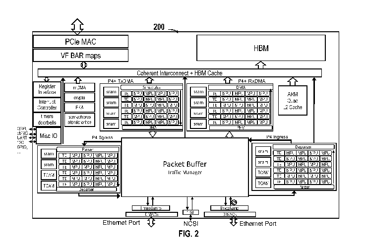
[0054] FIG. 2 shows another exemplary 10 device system 200 with described
programmable
device interface, in accordance with some embodiments of the invention. The
system 200 serves
as an example of implementing the P4 and extended P4 pipelines and various
other functions to
provide an improved network performance. In some cases, the device interface
may have
improved network performance by: not requiring PCIe bus register reads in the
packet transmit or
receive path; providing a single posted (non-blocking) PCIe bus register write
for packet
transmit; supporting for message signaled interrupts (MSI) and message
signaled interrupts-
extended (MSI-X) modes with driver-configurable interrupt moderation for high-
performance
interrupt processing; supporting I/0 queues with outstanding requests (e.g.,
up to 64k) per queue;
transmitting TCP segmentation Offload (TSO) with improved send size; providing
Transmission
Control Protocol(TCP)/User Datagram Protocol (UDP) checksum offload;
supporting for a
variable number of Receive Queues to support industry standard Receive Side
Scaling (RSS);
supporting SR-My with up to 255 virtual functions.
[0055] The 10 device system 200 may be the same 10 device as described in FIG.
1 and
implemented as a rack mounted device and comprise one or more Application
Specific Integrated
Circuits (ASICS) and/or boards with components mounted thereon. As shown in
FIG. 2, the
system 200 may comprise four advanced RISC machine (ARM) processors with
coherent Li and
L2 caches, a shared local memory system, flash non-volatile memory, DMA
engines, and
miscellaneous 10 devices for operation and debug. The ARM processors may
observe and
control all NIC resources via an address map. The ARM processor may implement
the P4
pipeline and the extended P4 pipeline as described later herein.
[0056] The system may comprise a host interface and a network interface. The
host interface
may be configured to provide communication link(s) with one or more hosts
(e.g., host servers).
The host interface block may also observe regions of the address space via
PCIe BAR maps to
expose NIC functions to a host system. In an example, the address map may be
initially created
12
CA 03091265 2020-08-13
WO 2019/164827 PCT/US2019/018544
according to the principles of ARM memory maps, ARM limited, which provides
SOC
addressing guidelines for a 34-bit memory map.
[0057] The network interface may support network connections or uplinks with a
computing
network that may be, for example, a local area network, wide area network and
various others as
described elsewhere herein. The physical link may be controlled by a
management agent (e.g.,
management entity 119) through the device driver. For example, the physical
link may be
configured via a "virtual link" associated with a device logical interface
(LIF).
[0058] All memory transactions in the system 200, including host memory, high
bandwidth
memory (HBM), and registers may be connected via a coherent network on a chip
(NOC) based
on IP from an external Systems. The NOC may provide cache coherent
interconnect between the
NOC masters, including P4 pipeline, extended P4 pipeline, DMA, PCIe, and ARM.
The
interconnect may distribute HBM memory transactions across a plurality (e.g.,
16) of HBM
interfaces using a programmable hash algorithm. All traffic targeting HBM may
be stored in the
NOC cache (e.g., 1 MB cache). The NOC cache may be kept coherent with the ARM
caches. The
NOC cache may be used to aggregate HBM write transactions which may be smaller
than the
cache line (e.g., size of 64 bytes), as the HBM is not efficient when
processing small writes. The
NOC cache may have high bandwidth, supporting up to 3.2 Tb/s operation as it
fronts the 1.6
Tb/s HBM.
[0059] The system may comprise an internal HBM memory system for running
Linux, storing
large data structures such as flow tables and other analytics, and providing
buffering resources
for advanced features including TCP termination and proxy, deep packet
inspection, storage
offloads, and connected FPGA functions. The memory system may comprise a HBM
module
which may support 4GB capacity or 8GB capacity, depending on package and HBM.
[0060] As mentioned above, the system may comprise a PCIe host interface. The
PCIe host
interface may support a bandwidth of, for example, 100 Gb/s per PCIe
connection (e.g., dual
PCIe Gen4x8 or single PCIe Gen3x16). A mechanism or a scheme to map resources
available at
the TO device to memory-mapped control regions associated with the virtual TO
devices may be
implemented by using a pool of configurable PCIe Base Address Registers (BARs)
coupled with
a resource mapping table to store mapping information for each virtual TO
device. The TO
resources provided by the TO device may be mapped to host addresses in the
framework of the
PCIe standard such that the same device drivers that are utilized to
communicate with physical
PCIe devices may be utilized to communicate with corresponding virtual PCIe
devices.
[0061] The TO device interface may comprise programmable registers. These
registers may
13
CA 03091265 2020-08-13
WO 2019/164827 PCT/US2019/018544
comprise, for example, PCIe base address registers (BARs) that may include a
first memory BAR
containing device resources (e.g., device command registers, doorbell
registers, interrupt control
registers, interrupt status registers, MSI-X interrupt table, MSI-X interrupt
pending bit array, etc.)
a second BAR containing device doorbells pages, and a third BAR for mapping a
controller
memory buffer.
[0062] The device command registers are a set of registers used for submitting
administrative
commands to the hardware or firmware. For example, the device command
registers may specify
a single-64 byte command and a single 16-byte completion response. This
register interface may
allow for a single command outstanding at a time. The device command doorbell
is a special
purpose doorbell used to signal a command is ready in the device command
registers.
[0063] The second BAR may contain doorbells pages. The general form of the
second BAR may
contain multiple LIFs with multiple doorbell pages per LIF. A network device
(i.e., TO device)
may have at least one LIF with at least one doorbell page. Any combination of
single/many LIFs
with single/many Doorbell Pages is possible and the driver may be prepared to
identify and
operate the different combinations. In an example, doorbell pages may be
presented on a 4k
stride by default to match a common system page size. The stride between
doorbell pages may be
adjusted in the virtual function device 113 to match the system page size
configuration setting in
the SR-My capability header in the parent physical function device 115. This
page size
separation allows protected independent direct access to a set of doorbell
registers by processes
by allowing each process to map and access a doorbell page dedicated for its
use. Each page may
provide the doorbell resources needed to operate the data path queue resources
for a LIF, while
protecting access to those resources from another process.
[0064] The doorbell register may be written by software to adjust a queue's
producer index.
Adjusting the producer index is the mechanism to transfer ownership of queue
entries in the
queue descriptor ring to the hardware. Some doorbell types, such as the Admin
Queue, Ethernet
Transmit Queue, and RDMA Send Queue, may cause the hardware queue to schedule
further
processing of the descriptors available in the queue. Other queue types, such
as Completion
Queues and Receive Queues, may require no further action from the hardware
queue after
updating the producer index.
[0065] The interrupt status register may contain a bit for each interrupt
resource of the device.
The register may have a bit set indicating the corresponding interrupt
resource has asserted its
interrupt. For example, bit 0 in Interrupt Status indicates interrupt resource
0 is asserted, bit 1
indicates interrupt resource 1 is asserted.
14
CA 03091265 2020-08-13
WO 2019/164827 PCT/US2019/018544
[0066] The controller memory buffer may be a region of general purpose memory
resident on the
JO device. The user or kernel driver may map in this controller memory BAR,
and build
descriptor rings, descriptors, and/or payload data in the region. A bit may be
added in the
descriptor to select whether the descriptor address field is interpreted as a
host memory address,
or as an offset relative to the beginning of the device controller memory
window. The extended
P4 program may set a designated bit (e.g., bit 63) of the address if it is a
host address, or clear the
bit and add the device controller memory base address to the offset when
building the TxDMA
operations for the DMA stage.
[0067] The MSI-X resources may be mapped through the first BAR and the format
may be
described by the PCIe Base Specification. The MSI-X interrupt table is a
region of control
registers that allows an OS to program MSI-X interrupt vectors on behalf of
the driver.
[0068] The MSI-X Interrupt Pending Bit Array (PBA) is an array of bits, one
for each MSI-X
interrupt supported by the device.
[0069] The JO device interface may support programmable DMA register tables,
descriptor
formats, and control register formats, allowing specialized VF interfaces and
user defined
behaviors. The JO device PCIe interface logic may be programmed to map control
registers and
NIC memory regions with programmable access permissions (e.g., read, write,
execute) to the
VF BARs.
[0070] FIG. 3A is a diagram shows an example 300 of an internal arrangement of
a PCIe
configuration register. As examples of the addresses, the device ID designates
a device number
specific to a vendor, the vendor ID designates the number of a manufacturer
(both offset 00h),
and the class code (offset 08h) designates a device attribute. Addresses
offset 10h-24h and 30h
are used for base address registers. Configuration software included in the SR-
PCIM can identify
a device by looking up the register values. The base address registers are
used by the
configuration software in the SR-PCIM for writing a base address when
allocating an address
space for an I/0 device. The device identification and related processes occur
during PCIe
configuration cycles. Such configuration cycles occur during system startup
and possibly after a
hot-plugging operation.
[0071] The transmission ring may include a ring buffer. FIG. 3B shows examples
of P4 defined
descriptor rings 301. In some cases, the memory structures of the JO device
interface may be
defined in the descriptor formats. In the example, the receive queue (RxQ)
descriptor may have
the following fields:
// Basic RxQ receive descriptor
CA 03091265 2020-08-13
WO 2019/164827 PCT/US2019/018544
header type rx desc t {
fields {
buffer addr : 64; //buffer address
buffer size : 14; // length of the buffer
flags : 2;
pad: 16;
// RxQ Configuration Registers
header type rxq config t {
ring base : 64;
ring size log : 4;
p index: 16; //producer index, set by doorbell register
c index: 16; // set by doorbell register
s index: 16; // saved (cache) index
enable: 1;
[0072] In the case of transmission queue, the transmission queue descriptor
may have a single
DMA address field for the first data buffer fragment to send. If there is only
one fragment, then
the single DMA address is sufficient to send the entire packet. In the case of
more than one
fragment, a transmit scatter-gather list may be used to describe the DMA
address and the length
of the subsequent fragments.
[0073] As mentioned above, the provided 10 device interface extends the P4
programmable
pipeline mechanism to the host driver. For example, P4 programmed DMA
interfaces may be
presented directly to host virtual functions and the processing entity (e.g.,
ARM CPU) of the
network device or the offload engine interfaces. The 10 device interface may
support up to 2048
or more PCIe virtual functions for direct container mapping with multiple
transmit and receive
queues. Combining the programmable 10 device interface with the P4 pipeline
features allows
the host virtual switch/NIC to be offloaded to the programmable network device
with improved
16
CA 03091265 2020-08-13
WO 2019/164827 PCT/US2019/018544
bandwidth and low latency.
Match processing unit (MPU)
[0074] In an aspect of the invention, a match processing unit (MPU) is
provided to process a data
structure. The data structure may comprise various types such as data packet,
a management
token, administrative command from a host, a processing token, a descriptor
ring and various
others. The MPU may be configured to perform various operations according to
the type of data
being processed or different purposes. For example, the operations may include
table-based
actions for processing packets, table maintenance operations such as writing a
timestamp to a
table or harvesting table data for export, administrative operations such as
creating new queues or
memory maps, gathering statistics, and various other operations such as
initiating a bulk data
processing that may result in writing any type of modified data to the host
memory.
[0075] In some embodiments, the MPU may process a data structure in order to
update the
memory based data structure or initiate an event. The event may involve
modifying a packet such
as modifying the PHV field of the packet as described elsewhere herein.
Alternatively, the event
may not relate to modifying or updating a packet. For instance, the event may
be administrative
operations such as creating new queues or memory maps, gathering statistics,
initiating a bulk
data processing that may result in writing any type of modified data to the
host memory, or
performing calculations on descriptor rings, scatter gather lists (SGLs).
[0076] FIG. 4 shows a block diagram of a match processing unit (MPU) 400, in
accordance with
embodiments of the invention. In some embodiments, the MPU unit 400 may
comprise multiple
functional units, memories and at least a register file. For example, the MPU
unit may comprise
an instruction fetch unit 401, a register file unit 407, a communication
interface 405, arithmetic
logic units (ALUs) 409 and various other functional units.
[0077] In the illustrated example, the MPU unit 400 may comprise a write port
or
communication interface 405 allowing for memory read/write operations. For
instance, the
communication interface may support packets written to or read from an
external memory (e.g.,
high bandwidth memory (HBM) of a host device) or an internal static random
access memory
(SRAM). The communication interface 405 may employ any suitable protocol such
as Advanced
Microcontroller Bus Architecture (AMBA) Advanced extensible Interface (AXI)
protocol. AXI
is a bus protocol for a high-speed/high-end on-chip bus protocol and has
channels associated with
read, write, address, and write response, which are respectively separated,
individually operated,
and have transaction properties such as multiple-outstanding address or write
data interleaving.
The AXI interface 405 may include features that support for unaligned data
transfers using byte
17
CA 03091265 2020-08-13
WO 2019/164827 PCT/US2019/018544
strobes, burst based transactions with only start address issued, separate
address/control and data
phases, issuing of multiple outstanding addresses with out of order responses,
and easy addition
of register stages to provide timing closure. For example, when the MPU
executes a table write
instruction, the MPU may track which bytes have been written to (a.k.a. dirty
bytes) and which
remain unchanged. When the table entry is flushed back to the memory, the
dirty byte vector may
be provided to AXI as a write strobe, allowing multiple writes to safely
update a single table data
structure as long they do not write to the same byte. In some cases, dirty
bytes in the table need
not be contiguous and the MPU may only write back a table if at least one bit
in the dirty vector
is set. Though packet data is transferred according the AXI protocol in the
packet data
communication on-chip interconnect system according to the present exemplary
embodiment in
the present specification, it can also be applied to a packet data
communication on-chip
interconnect system operating by other protocols supporting a lock operation,
such as Advanced
High-performance Bus (AHB) protocol or Advanced Peripheral Bus (APB) protocol
in addition
to the AXI protocol.
[0078] The MPU 400 may comprise an instruction fetch unit 401 configured to
fetch instruction
set from a memory external to the MPU based on the input table result or at
least a portion of the
table result. The instruction fetch unit may support branches and/or linear
code paths based on
table results or a portion of a table result provided by a table engine. In
some cases, the table
result may comprise table data, key data and/or a start address of a set of
instructions/program.
Details about the table engine are described later herein. In some
embodiments, the instruction
fetch unit 401 may comprise an instruction cache 403 for storing one or more
programs. In some
cases, the one or more programs may be loaded into the instruction cache 403
upon receiving the
start address of the program provided by the table engine. In some cases, a
set of instructions or a
program may be stored in a contiguous region of a memory unit, and the
contiguous region can
be identified by the address. In some cases, the one or more programs may be
fetched and loaded
from an external memory via the communication interface 405. This provides
flexibility to allow
for executing different programs associated with different types of data using
the same
processing unit. In an example, when a management packet header vector (PHV)
injected into the
pipeline, for example to perform administrative table direct memory access
(DMA) operations or
entry aging functions (i.e., adding timestamps), one of the management MPU
programs may be
loaded to the instruction cache to execute the management function. The
instruction cache 403
can be implemented using various types of memories such as one or more SRAMs.
[0079] The one or more programs can be any programs such as P4 programs
related to reading
table, building headers, DMA to/from memory regions in HBM or in the host
device and various
18
CA 03091265 2020-08-13
WO 2019/164827 PCT/US2019/018544
other actions. The one or more programs can be executed in any stage of a
pipeline as described
elsewhere herein.
[0080] The MPU 400 may comprise a register file unit 407 to stage data between
the memory
and the functional units of the MPU, or between the memory external to the MPU
and the
functional units of the MPU. The functional units may include, for example,
ALUs, meters,
counters, adders, shifters, edge detectors, zero detectors, condition code
registers, status registers,
and the like. In some cases, the register file unit 407 may comprise a
plurality of general purpose
registers (e.g., RO, R1, Rn) which may be initially loaded with metadata
values then later used
to store temporary variables within execution of a program until completion of
the program. For
example, the register file unit 407 may be used to store SRAM addresses,
ternary content
addressable memory (TCAM) search values, ALU operands, comparison sources, or
action
results. The register file unit of a stage may also provide data/program
context to the register file
of the subsequent stage, as well as making data/program context available to
the next stage's
execution data path (i.e., the source registers of the next stage's adder,
shifter, and the like). In
one embodiment, each register of the register file is 64 bits and may be
initially loaded with
special metadata values such as hash value from table, lookup, packet size,
PHV timestamp,
programmable table constant and the like, respectively.
[0081] In some embodiments, the register file unit 407 may also comprise
comparator flags unit
(e.g., CO, Cl, Cn) configured to store comparator flags. The comparator
flags can be set by
calculation results generated by the ALU which in return is compared with
constant values in an
encoded instruction to determine a conditional branch instruction. In an
embodiment, the MPU
may comprise eight one-bit comparator flags. However, it should be noted that
MPU may
comprise any number of comparator flag units each of which may have any
suitable length.
[0082] The MPU 400 may comprise one or more functional units such as the ALU
409. The
ALU may support arithmetic and logical operations on the values stored in the
register file unit
407. The results of the ALU operations (e.g., add, subtract, AND, OR, XOR,
NOT, AND NOT,
shift, and compare) may then be written back to the register file. The
functional units of the MPU
may, for example, update or modify fields anywhere in a PHV, write to memory
(e.g., table
flush), or perform operations that are not related to PHV update. For example,
the ALU may be
configured to perform calculations on descriptor rings, scatter gather lists
(SGLs), and control
data structures loaded into the general purpose registers from the host
memory.
[0083] The MPU 400 may comprise various other functional units such as meters,
counters,
action insert unit and the like. For example, the ALU may be configured to
support P4 compliant
19
CA 03091265 2020-08-13
WO 2019/164827 PCT/US2019/018544
meters. A meter is a type of action executable on a table match used to
measure data flow rates.
A meter may include a number of bands, typically two or three, each of which
has a defined
maximum data rate and optional burst size. Using a leaky bucket analogy, a
meter band is a
bucket filled by the packet data rate and drained at a constant allowed data
rate. Overflow occurs
if the integration of data rate exceeding quota is larger than the burst size.
Overflowing one band
triggers activity into the next band, which presumably allows a higher data
rate. In some cases, a
field of the packet may be remarked as a result of overflowing the base band.
This information
might be used later to direct the packet to a different queue, where it may be
more subject to
delay or dropping in case of congestion. The counter may be implemented by the
MPU
instructions. The MPU may comprise one or more types of counters for different
purposes. For
example, the MPU may comprise performance counters to count MPU stalls. The
action insert
unit may be configured to push the register file result back to the PHV for
header field
modifications.
[0084] The MPU may be capable of locking a table. In some case, a table being
processed by a
MPU may be locked or marked as "locked" in the table engine. For example,
while an MPU has
a table loaded into its register file, the table address may be reported back
to the table engine,
causing future reads to the same table address to stall until the MPU has
released the table lock.
For instance, the MPU may release the lock when an explicit table flush
instruction is executed,
the MPU program ends, or the MPU address is changed. In some cases, an MPU may
lock more
than one table addresses, for example, one for the previous table write-back
and another address
lock for the current MPU program.
MPU pipelining
[0085] A single MPU may be configured to execute instructions of a program
until completion of
the program. Alternatively or additionally, multiple MPUs may be configured to
execute a
program. In some embodiments, a table result may be distributed to multiple
MPUs. The table
result may be distributed to multiple MPUs according to a MPU distribution
mask configured for
the tables. This provides advantages to prevent data stalls or mega packets
per second (MPPS)
decrease when a program is too long. For example, if a PHV requires four table
reads in one
stage, then each MPU program may be limited to only eight instructions in
order to maintain a
100 NIPPS if operating at a frequency of 800 MHz in which scenario multiple
MPUs may be
desirable.
[0086] Any number of MPUs may be used for executing a program in order to meet
a desirable
performance. For instance, at least two, three, four, five, six, seven, eight,
nine, or ten MPUs may
CA 03091265 2020-08-13
WO 2019/164827 PCT/US2019/018544
be used to execute a program. Each MPU may execute at least a portion of the
program or a
subset of the instruction set. The multiple MPUs may perform the execution
simultaneously or
sequentially. Each MPU may or may not perform the same number of instructions.
The
configurations may be determined according to the length of program (i.e.,
number of
instructions, cycles) and/or number of available MPUs. In some case, the
configuration may be
determined by an application instruction received from a main memory of a host
device operably
coupled to the plurality of MPUs.
P4 pipelines
[0087] In one aspect, a flexible, high performance match action pipeline which
can execute a
wide range of P4 programs is provided. The P4 pipeline can be programmed to
provide various
features, including, but not limited to, routing, bridging, tunneling,
forwarding, network ACLs,
L4 firewalls, flow based rate limiting, VLAN tag policies, membership,
isolation, multicast and
group control, label push/pop operations, L4 load balancing, L4 flow tables
for analytics and
flow specific processing, DDOS attack detection, mitigation, telemetry data
gathering on any
packet field or flow state and various others. FIG. 5 shows a block diagram of
an exemplary P4
ingress or egress pipeline (PIP pipeline) 500 in accordance with embodiments
of the invention.
[0088] In some embodiments, the provided invention may support a match +
action pipeline. The
programmer or compiler may decompose the packet processing program into a set
of dependent
or independent table lookup and action processing stages (i.e., match +
action) which are mapped
onto the table engine and MPU stages respectively. The match + action pipeline
may comprise a
plurality of stages. For example, a packet entering the pipeline may be first
parsed by a parser
(e.g., parser 507) according to the packet header stack specified by a P4
program. This parsed
representation of the packet may be referred to as parsed header vector. The
parsed header vector
may then be passed through stages (e.g., stages 501-1, 501-2, 501-3, 501-4,
501-5, 501-6) of
ingress match + action pipeline, wherein each stage is configured to match one
or more parsed
header vector fields to tables, then updates the packet header vector (PHV)
and/or table entries
according to the actions specified by the P4 program. In some instances, if
the required number
of stages exceeds the implemented number of stages, a packet may be
recirculated for additional
processing. In some cases, the packet payload may travel in a separate first-
in-first-out (FIFO)
queue until it is reassembled with its PHV in the de-parser (e.g., de-parser
509). The de-parser
may rewrite the original packet according to the PHV fields which have been
modified (e.g.,
added, removed, or updated). In some cases, the packet processed by the
ingress pipeline may be
placed in a packet buffer for scheduling and possible replication. In some
cases, once the packet
21
CA 03091265 2020-08-13
WO 2019/164827 PCT/US2019/018544
is scheduled and leaves the packet buffer, it may be parsed again to create an
egress parsed
header vector. The egress parsed header vector may be passed through a
sequence of stages of
match + action pipeline in a similar fashion of the ingress match + action
pipeline, after which a
final de-parser operation may be3 executed before the packet is sent to its
destination interface or
recirculated for additional processing.
[0089] In some embodiments, the ingress pipeline and egress pipeline may be
implemented using
the same physical block or processing unit pipeline. In some embodiments, the
PIP pipeline 500
may comprise at least one parser 507 and at least one de-parser 509. The PIP
pipeline 500 may
comprise multiple parsers and/or multiple de-parsers. The parser and/or de-
parser may be a P4
compliant programmable parser or de-parser. In some cases, the parser may be
configured to
extract packet header fields according to P4 header definitions and place them
in the packet
header vector (PHV). The parser may select from any fields within the packet
and align the
information from the selected fields to create a packet header vector. In some
cases, after passing
through a pipeline of match + action stages, the de-parser block may be
configured to rewrite the
original packet according to the updated PHV.
[0090] The packet header vector (PHV) produced by the parser may have any size
or length. For
example, the PHV may be a least 512 bits, 256 bits, 128 bits, 64 bits, 32
bits, 8 bits or 4 bits. In
some cases, when a long PHV (e.g., 6 Kb) is desired to contain all relevant
header fields and
metadata, a single PHV may be time division multiplexed (TDM) across several
cycles. This
TDM capability provides benefit allowing the described invention to support
variable length
PHVs, including very long PHVs to enable complex features. A PHV length may
vary as the
packet passes through the match + action stages.
[0091] The PIP pipeline may comprise a plurality of match + action stages.
After the parser 507
produces the PHV, the PHV may be passed through the ingress match + action
stages. In some
embodiments, the PIP pipeline may be implemented using multiple stage units
501-1, 501-2,
501-3, 501-4, 501-5, 501-6, each of which may comprise a table engine 505 and
multiple MPUs
503. The MPU 503 can be same as the MPU as described in FIG. 4. In the
illustrated example,
four MPUs are used in one stage unit. However, any other number of MPUs, such
as at least one,
two, three, four, five, six, seven, eight, nine, or ten can be utilized or
grouped with a table engine.
[0092] A table engine 505 may be configured to support per-stage table match.
For example, the
table engine 505 may be configured to hash, lookup, and/or compare keys to
table entries. The
table engine 505 may be configured to control table match process by
controlling the address and
size of the table, PHV fields to use as a lookup key, and MPU instruction
vector which defines
22
CA 03091265 2020-08-13
WO 2019/164827 PCT/US2019/018544
the P4 program associated with the table. A table result produced by the table
engine may be
distributed to the multiple MPUs 503.
[0093] The table engine 505 may be configured to control a table selection. In
some cases, upon
entering a stage, the PHV may be examined to select which table(s) to enable
for the arriving
PHV. Table selection criteria may be determined based on the information
contained in the PHV.
In some cases, a match table may be selected based on packet type information
related to a
packet type associated with the PHV. For instance, the table selection
criteria may be based on
packet type or protocols (e.g., Internet Protocol version 4 (IPv4), Internet
Protocol version 6
(IPv6) and Multiprotocol Label Switching (MPLS)) or the next table ID as
determined by the
preceding stage or the previous stage. In some cases, the incoming PHV may be
analyzed by the
table selection logic, which then generates a table selection key and compares
the result using a
TCAM to select the active tables. The table selection Key may be used to drive
table hash
generation, table data comparison, and associated data into the MPUs.
[0094] In some embodiments, the table engine 505 may comprise a hash
generation unit. The
hash generation unit may be configured to generate a hash result off a PHV
input and the hash
result may be used to conduct a DMA read from a DRAM or SRAM array. In an
example, the
input to the hash generation unit may be masked according to which bits in the
table selection
key contribute to the hash entropy. In some cases, the same mask may be used
by the table
engine for comparison with the returning SRAM read data. In some instances,
the hash result
may be scaled according to the table size, then the table base offset may be
added to create the
memory index. The memory index may be sent to the DRAM or SRAM array and to
perform the
read.
[0095] In some cases, the table engine 505 may comprise a TCAM control unit.
The TCAM
control unit may be configured to allocate memory to store multiple TCAM
search tables. In an
example, a PHV table selection key may be directed to a TCAM search stage
before a SRAM
lookup. TCAM search tables can be configured to be up to 1024 bits wide and as
deep as TCAM
resources permit. In some cases, multiple TCAM tables may be carved from the
shared quadrant
TCAM resources. The TCAM control unit may be configured to allocate TCAMs to
individual
stages so that to prevent TCAM resource conflicts, or allocate TCAM into
multiple search tables
within a stage. The TCAM search index results may be forwarded to the table
engine for SRAM
lookups.
[0096] The PIP pipeline 500 may comprise multiple stage units 501-1, 501-2,
501-3, 501-4, 501-
5, 501-6. The PIP pipeline may comprise any number of stage units such as at
least two, three,
23
CA 03091265 2020-08-13
WO 2019/164827 PCT/US2019/018544
four, five, six, seven, eight, nine, ten sage units that can be used within
the PIP pipeline. In the
illustrated example, six match + action stages units 501-1, 501-2, 501-3, 501-
4, 501-5, 501-6 are
grouped into a set. The set of stages units may share a common set of SRAMs
511 and TCAMs
513. The SRAMs 511 and TCAMs 513 may be component of the PIP pipeline. This
arrangement
may allow the six stage units to divide match table resources in any suitable
proportion which
provides convenience to the compiler and easing the complier's task of
resource mapping. Any
suitable number of SRAM resources and any suitable number of TCAM resources
may be used
by each PIP pipeline. For example, the illustrated PIP pipeline may be coupled
to ten SRAM
resources and four or eight TCAM resources. In some instances, TCAMs may be
fused vertically
or horizontally for a wider or deeper search.
Extended P4 pipelines
[0097] In one aspect, the provided invention may support an extended P4
programmable pipeline
to allow for direct interfacing with the host driver. The extended P4
programmable pipeline
implements the 10 device interface as described above. For example, the P4
programmed DMA
interfaces may be directly coupled to the host virtual functions (VFs) as well
as advanced RISC
machine (ARM) CPU or offload engine interfaces. The extended P4 pipeline may
handle
required DMA operations and loops. The extended P4 pipeline may include
features, including
but not limited to, stateless NIC offloads such as TCP segmentation offload
(TSO) and Receive
Side Scaling (RSS); storage exchange table-style transaction servicing in the
extended P4
pipeline; fine grained load balancing decisions that can be extended to
individual data structures
of performance critical applications, such as DPDK or key value matching; TCP
flow termination
and initiation for proxy services; RDMA over converged Ethernet (RoCE) and
similar remote
direct memory access (RDMA) protocol support; custom descriptor and SGL
formats can be
specified in P4 to match data structures of performance critical applications;
new device and VF
behaviors can be modelled using P4 programs coupled with host driver
development, and various
other features.
[0098] Data may be transmitted between the packetized domain in the P4
pipeline to/from the
memory transaction domain in the host and NIC memory systems. This packet to
memory
transaction conversion may be performed by the extended P4 pipelines that
include DMA write
(TxDMA) and/or DMA read (RxDMA) operations. The extended P4 pipeline includes
TxDMA
may also be referred to as Tx P4 or TxDMA and the extended P4 pipeline
includes RxDMA may
also be referred to as Rx P4 throughout this specification. The extended P4
pipelines may
comprise the same match + action stages in the P4 pipeline, and a payload DMA
stage at the end
24
CA 03091265 2020-08-13
WO 2019/164827 PCT/US2019/018544
of the pipeline. Packets may be segmented or reassembled into data buffers or
memory regions
(e.g., RDMA registered memory) according to the extended P4 programs. The
payload DMA
stage may be a P4 extension which enables the programmable P4 network pipeline
extended to
the host memory system and driver interface. This P4 extension allows custom
data structures
and applications interactions to be tailored to application or container
needs.
[0099] The match table utilized in the extended P4 pipeline may be
programmable tables. A
stage of an extended P4 pipeline may include multiple programmable tables
which may exist in
SRAM, NIC DRAM, or host memory. For example, host memory structures may
include
descriptor rings, SGLs, and control data structures which can be read into the
register file unit of
the MPU for calculations. The MPU may add PHV commands to control DMA
operations to and
from host and NIC memory, and insert DMA commands into the PHV for execution
by the
payload DMA stage. The extended P4 programs may include, for example,
completion queue
events, interrupts, timer set, and control register writes and various others
programs.
[00100] FIG. 6 illustrates an exemplary extended pipeline of stages for
Ethernet packet
transmission (i.e., Tx P4 pipeline) 600. In the example, a table engine of
stage 0 may fetch the
queue state (e.g., Q state) table for processing by the MPUs of stage 0. In
some cases, the queue
state may also contain an instruction offset address based on the type of
queue pairs in order to
speed MPU processing. Other separate Tx P4 programs can be written for an
Ethernet Tx queue,
an RDMA command queue, or any new type of transmit DMA behavior customized to
a
particular application. The number of supported Tx queue pairs may be
determined based on
hardware scheduler resources assigned to each queue pair. As mentioned above,
the PHV may be
passed through each stage in which match + action programs may be executed by
the stage unit
associated therewith. The MPU of the final stage (e.g., stage 5) may insert
DMA commands into
the PHV for execution by the payload DMA stage (e.g., PDMA).
[00101] FIG. 7 and FIG. 8 show exemplary Rx P4 pipeline 700 and Tx P4
pipeline 800 in
accordance with embodiments of the invention. The Rx P4 stages and/or Tx P4
stages may be
generally similar to the P4 pipeline stages as described elsewhere herein with
a few different
features. In some cases, the extended P4 stages may not use TCAM resources and
may use less
SRAM resources than P4 stages. In some cases, the extended P4 pipeline may
comprise different
number of stages than the P4 pipeline, by having a payload DMA stage at the
end of the pipeline.
In some cases, the extended P4 pipeline may have a local PHV recirculate data
path that may not
use packet buffer.
[00102] Referring to the Rx P4 pipeline (i.e., RxDMA P4 pipeline) as shown
in FIG. 7,
CA 03091265 2020-08-13
WO 2019/164827 PCT/US2019/018544
the Rx P4 pipeline may comprise multiple stage units 701-1, 701-2, ... 701-n
each of which may
have the same physical block of the stage unit as described in FIG. 5. The
number of stage units
in the Rx P4 pipeline may or may not be the same as the number of stage units
of a P4 pipeline as
mentioned above. In an example, a packet may be passed to the Rx P4 pipeline
from a P4
networking pipeline which may include P4 forwarding, isolation, multicast, L4
security, and
other network features.
[00103] In some embodiments, the Rx P4 pipeline 700 may comprise a PHV
splitter block
703 configured to generate an RxDMA PHV. For example, the metadata fields of
the PHV (e.g.,
logical interfaces (LIF) ID) as required by the RxDMA may be passed from the
P4 network
pipeline through the packet buffer as a contiguous block of fields prepended
to the packet. Before
entering the first stage of RxDMA P4 pipeline, the PHV splitter block 703 may
extract the
prepended metadata and place it in the RxDMA PHV. The PHV splitter block 703
may maintain
a count of number of PHVs that are currently in the RxDMA pipeline, as well as
a count of
number of packet payload bytes that are in the pipeline. In some cases, when
either the PHV
count or the total packet byte count exceeds a high water mark, the PHV
splitter block 503 may
stop accepting new packets from the packet buffer. This provides benefit to
ensure that packets
recirculated from the payload DMA block 705 have priority to be processed and
exit the pipeline.
[00104] The Rx P4 pipeline may comprise a packet DMA block 705 configured
to control
ordering between dependent events. The packet DMA block may also be referred
to as payload
DMA block. A packet data may be sent in a FIFO to the packet DMA block 705 to
await DMA
commands created in the Rx P4 pipeline. The packet DMA block at the end of the
Rx P4 pipeline
may execute the packet DMA write commands, DMA completion queue (CQ) write
commands,
interrupt assertion writes, and doorbell writes in the order the DMA commands
are placed in the
PHV.
[00105] Referring to the Tx P4 pipeline 800 shown in FIG. 8, the Tx P4
pipeline may
comprise multiple stage units 801-1, 801-2, ... 801-k each of which may have
the same physical
block of the stage unit as described in FIG. 7. The number of stage units in
the Tx P4 pipeline
may or may not be the same as the number of stage units of an Rx P4 pipeline
as described
above. In an example, packets may be transmitted from a host or NIC memory
using the Tx P4
pipeline. The Tx queue scheduler may select the next queue for service and
submits the LIF, QID
to the beginning of the Tx P4 pipeline.
[00106] The Tx P4 pipeline may comprise a null PHV block 803 configured to
generate
address to be read by the table engine in stage 0. The null PHV block 803 may
also insert
26
CA 03091265 2020-08-13
WO 2019/164827 PCT/US2019/018544
information such as LIF or LIF type to the intrinsic fields of the PHV. The
null PHV block 803
may also insert recirculated PHVs back into the pipeline from the last stage
of the Tx P4 pipeline,
as well as insert software generated PHVs. The Tx P4 pipeline may comprise a
packet DMA
block 805 similar to the packet DMA block as described in FIG. 7.
[00107] In some embodiments, Tx DMA pipeline, Rx DMA pipeline, and P4
pipeline may
be capable of inserting software generated PHVs before the first stage of the
respective pipeline.
Software may use generated PHVs to launch MPU programs, perform table
modifications, or
launch DMA commands from the extended P4 pipeline.
[00108] In an aspect, a system comprising the Tx DMA pipeline, Rx DMA
pipeline, and
P4 pipeline and other components may be provided. The system may support
extended P4
pipeline based host interface features (e.g., DMA operations and loops),
provide improved
network performance (e.g., increased MMPS with reduced data stalls), fault
detection and
isolation, P4 based network features (e.g., routing, bridging, tunneling,
forwarding, network
ACLs, L4 firewalls, flow based rate limiting, VLAN tag policies, membership,
isolation,
multicast and group control, label push/pop operations, L4 load balancing, L4
flow tables for
analytics and flow specific processing, DDOS attach detection, mitigation,
telemetry data
gathering on any packet field or flow state), security features and various
others.
[00109] FIG. 9 illustrates an example of an extended transmission pipeline
(i.e., TxDMA
pipeline) 900. The provided TO device interface may support the TxDMA pipeline
operations to
transmit packets from a host system or NIC memory. The TO device interface may
have
improved performance such as a 16 reads per stage (i.e., 500 nsec host
latency), 32 MPPS or
higher for direct packet processing, and reduced latency. The provided TO
device interface may
comprise other features such as flexible rate limit controls. For example,
logical interfaces (LIFs)
can be independently rate limited by the Tx scheduler. Each LIF may have a
private qstate array
with a programmable base address in HBM and a programmable number of queues.
The device
interface may support a maximum of 2K or more LIFs. A LIF may contain eight or
more queue
types, with a programmable number of queues per queue type. For example, a
qstate array may
have a separate base address in HBM. This allows each LIF to scale the number
and type of
queue pairs it owns independently, up to a maximum array size determined at
the time of virtual
function creation. There may be one or more qstate types (e.g., eight qstate
types) within a qstate
array. Each type may have an independent entry size control as well as an
independent number of
entries. This allows each LIF to have a flexible mixture of queues of
different types.
[00110] As aforementioned, the TO device interface may be a highly
optimized ring based
27
CA 03091265 2020-08-13
WO 2019/164827 PCT/US2019/018544
1/0 queue interface. The extended P4 programs can be used to rate limit to a
much finer
granularity than the scheduler based rate limiter. An extended P4 program may
rate limit to
individual queue pairs using time and bucket data that are stored in qstate.
The extended P4 rate
limiting can be applied in the presence of scheduler (per-LIF) rate limiting,
allowing per-VM or
per-interface rates to be applied while per-queue limits enforce congestion or
other fine-grained
rate control. For example, the extended P4 rate limit programs may set XOFF
status to a primary
data transmission ring while leaving other rings for timers, administrative or
congestion message
transmit. In an exemplary process to implement a per-queue rate limited in the
extended P4
pipeline, the program may first determine if the current queue is under or
over its target rate. If
determined to be over its target rate, the program may drop the current
scheduler token and set a
timer resource to re-schedule the queue at a time in the future calculated
according to the current
token level and rate. Next, the program may disable the queue's scheduler bit,
but only for the
rings in the flow controlled COS. The queue may not be scheduled again until a
new doorbell
event occurs for the ring, even if work remains to be done for the primary
data transmission ring.
[00111] The TxDMA pipeline 900 as shown in FIG. 9 may comprise a pipeline
of stage
units 901-1, 901-2, ... 901-8 and a payload DMA block 902. The multiple stage
units 901-1, 901-
2, ... 901-8 each of which may have the same physical block of the stage unit
as described in
FIG. 8. In an example, packets may be transmitted from a host or NIC memory
using the
TxDMA pipeline. The Tx queue scheduler may select the next queue for service
and submits the
LIF, QID to the beginning of the TxDMA pipeline.
[00112] In some cases, a single queue may include up to eight or more
rings to allow
multiple event signaling options. Queues which are exposed to direct host
control may contain at
least one host accessible ring, typically the primary descriptor ring required
by the queue type.
Host access to the ring p index may be mapped through a doorbell. The
illustrated example
shows multiple stages for implementing Virtio programs. A table engine (TE) of
stage 0 may
fetch the queue state (e.g., Q state) table for processing by the MPUs of
stage 0. In some cases,
the queue state may also contain an instruction offset address based on the
type of queue pairs in
order to speed MPU processing. Other separate TxDMA programs can be written
for an Ethernet
Tx queue, an RDMA command queue, or any new type of transmit DMA behavior
customized to
a particular application. The number of supported Tx queue pairs may be
determined based on
hardware scheduler resources assigned to each queue pair.
[00113] It is noted that various embodiments can be used in conjunction
with one or more
types of wireless or wired communication signals and/or systems, for example,
radio frequency
28
CA 03091265 2020-08-13
WO 2019/164827 PCT/US2019/018544
(RF), infrared (IR), frequency-division multiplexing (FDM), orthogonal FDM
(OFDM), time-
division multiplexing (TDM), time-division multiple access (TDMA), extended
TDMA (E-
TDMA), general packet radio service (GPRS), extended GPRS, code-division
multiple access
(CDMA), wideband CDMA (WCDMA), CDMA 2000, multi-carrier modulation (MDM),
discrete multi-tone (DMT), Bluetooth , ZigBeeTM, or the like. Embodiments of
the invention
may be used in various other devices, systems, and/or networks.
[00114] While preferred embodiments of the present subject matter have
been shown and
described herein, it will be obvious to those skilled in the art that such
embodiments are provided
by way of example only. Numerous variations, changes, and substitutions will
now occur to
those skilled in the art without departing from the invention. It should be
understood that various
alternatives to the embodiments of the subject matter described herein may be
employed in
practicing the invention.
29