Note : Les descriptions sont présentées dans la langue officielle dans laquelle elles ont été soumises.
AUDIO AMPLIFIER ASSEMBLIES, PROCESSES, AND METHODS
[0001]
TECHNICAL FIELD
[0002] The disclosed technology relates to audio amplifiers.
BACKGROUND
[0003] Most professional audio amplifiers are limited in the range of
speaker loads they
can drive to full-rated power based on the maximum current the amplifier's
transistors can
conduct or the maximum voltage on the power supply rails that the transistors
can block.
Amplifier configurations have been developed to increase the range of speakers
loads that
can be driven by selectively summing channels together in parallel or by
connecting
channels together in a bridge tied load (BTL) configuration. One example of
such a
configurable amplifier is disclosed in U.S. Patent No. 9,543,913. The
technology disclosed
in the '913 patent is referred to below as Fast Amplitude and Summing
Technology (FAST).
[0004] The technology described herein seeks to improve upon the FAST by,
among
other things, making it easier for a user to connect speakers to an amplifier.
SUMMARY
[0005] As will be discussed in detail below, the disclosed technology
relates to an audio
amplifier having one or more channels where each channel includes two sub-
channels. A
first switch selectively connects an output of a second sub-channel to the
1
Date recue/ date received 2021-12-22
CA 03091825 2020-08-19
WO 2019/165317 PCMJS2019/019307
same speaker terminal that is connected to an output of the first sub-channel
such that the
outputs of the first and second sub-channels can drive a speaker load in
parallel The first
switch can also selectively connect the output of the second sub-channel to a
second
speaker terminal such that the first and second sub-channels can drive the
speaker in a
bridge tied load (BTL) configuration. A second switch of the channel
selectively connects
a ground of the second sub-channel to the second speaker terminal when the
speaker is
to be driven in parallel or can be set to a no connection position when the
speaker is to be
driven in the BTL configuration.
[0006] A processor or logic circuitry in the amplifier is configured to set
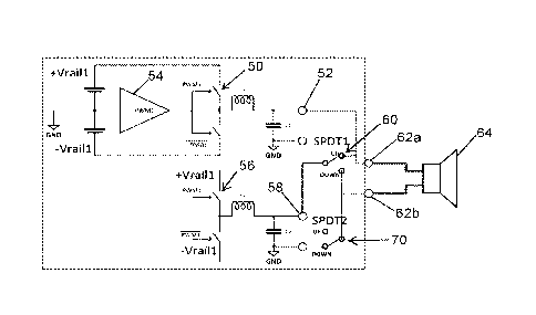
the position of
the first and second switches based on information received or detected
regarding the
impedance and power rating of a speaker load that is connected to the first
and second
speaker terminals.
BRIEF DESCRIPTION OF THE DRAWINGS
[0007] Figure 1 is a schematic of a typical class D audio amplifier output
stage in an
HB (Half-Bridge) configuration (prior art).
[0008] Figure 2 is a schematic of a conventional FB (Full-Bridge) class D
audio
amplifier topology, which may be referred to as a "BTL" (Bridge-Tied-Load)
configuration
(prior art).
[0009] Figure 3 is a schematic of an external BTL traditional coupling
(prior art).
[0010] Figure 4 is a schematic view of an amplifier including Flexible
Amplifier
Summing Technology ("FAST") for combining channels (prior art).
[0011] Figure 5 is a schematic view of an implementation of the disclosed
technology
with an amplifier having two Single Pole Double Throw (SPDT) switches in a
Current
Doubling ("CD") configuration.
[0012] Figure 6 is a schematic of an embodiment of the amplifier of Figure
5 in a
Voltage Doubling ("VD") configuration.
2
CA 03091825 2020-08-19
WO 2019/165317 PCMJS2019/019307
[0013] Figure 7 is a schematic of an embodiment of the amplifier of Figure
5 in a
Load Disconnect ("LD") configuration.
[0014] Figure 8 is a schematic of an upper amplifier in the "VD"
configuration, while a
redundant, lower amplifier is in the "LD" configuration.
[0015] Figure 9 is a schematic of an amplifier in a Rail Discharge ("RD")
configuration.
[0016] Figure 10 is a schematic of an amplifier channel or amplifier "unit"
according to
at least one embodiment of the disclosed technology comprising a Pulse
Modulation
configuration circuit routing externally provided Pulse Modulation signals or
internally
generated Pulse Modulation signals to first and second sub-channels within the
amplifier
channel.
[0017] Figure 11 is a schematic of an amplifier unit with a sub-channel
receiving a
non-inverted PWM in a load configuration set to "CD" or parallel. An output
SPDT saves
one set of two speaker terminals (and an input signal connection).
[0018] Figure 12 is a schematic of an amplifier unit with a sub-channel
receiving an
inverted PWM in a full-bridge coupling of the two internal sub-channels.
[0019] Figure 13 is a schematic of an amplifier unit with two amplifier
channels
having two power supply units (PSUs) that are not co-referenced (i.e. do not
share a
common ground). The two amplifier channels (units) can be each-other's
redundant
backup.
[0020] Figure 14 is a schematic of an amplifier unit in a rail discharge
(RD)
configuration that keeps the speaker load disconnected, while providing an
appropriate
PWM signal for discharging the rails into a near-short (some parasitic
resistance will cause
power dissipation depending on the parasitic resistance in the components and
traces
around the loop).
3
CA 03091825 2020-08-19
WO 2019/165317 PCT/US2019/019307
[0021]
Figure 15 is simplified diagram of an amplifier in accordance with aspects of
the disclosed technology showing identical universal physical wire connections
regardless
of the chosen internal configuration.
[0022]
Figure 16 is a block diagram of an amplifier including a processor configured
to set the configuration of the sub-channels in accordance with a detected
impedance of a
speaker load in accordance with some embodiments of the disclosed technology.
[0023]
Figures 17 shows an amplifier topology that allows subchannels to be stacked
in accordance with some embodiments of the disclosed technology.
[0024]
Embodiments of the audio amplifier, system and methods introduced herein
may be better understood by referring to the following Detailed Description in
conjunction
with the accompanying drawings.
DETAILED DESCRIPTION
[0025]
Various examples of the audio amplifiers, systems and methods introduced
above will now be described in further detail. The following description
provides specific
details for a thorough understanding and enabling description of these
examples. One
skilled in the relevant art will understand, however, that the techniques
discussed herein
may be practiced without many of these details. Likewise, one skilled in the
relevant art
will also understand that the technology can include many other features not
described in
detail herein. Additionally, some well-known structures or functions may not
be shown or
described in detail below so as to avoid unnecessarily obscuring the relevant
description.
[0026] The
headings provided herein are for convenience only and do not
necessarily affect the scope or meaning of the claimed embodiments. Further,
the
drawings have not necessarily been drawn to scale. For example, the dimensions
of
some of the elements in the figures may be expanded or reduced to help improve
the
understanding of the embodiments.
Moreover, while the disclosed technology is
amenable to various modifications and alternative forms, specific embodiments
have been
shown by way of example in the drawings and are described in detail below. The
intention, however, is not to limit the embodiments described. The embodiments
are
4
CA 03091825 2020-08-19
WO 2019/165317 PCMJS2019/019307
intended to cover all modifications, equivalents, and alternatives falling
within the scope of
the embodiments.
[0027] The terminology used below is to be interpreted in its broadest
reasonable
manner, even though it is being used in conjunction with a detailed
description of some
specific examples of the embodiments. Indeed, some terms may even be
emphasized
below; however, any terminology intended to be interpreted in any restricted
manner will
be overtly and specifically defined as such in this section.
[0028] New rack-amplifiers (or other professional audio amplifiers
including "Plate-
amps" for powered speakers) today are mostly implemented using a class D
topology with
pulse modulation, such as Pulse Width Modulation ("PWM"). The benefit of class
D (vs.
classes A, B, A/B, H, etc.) are the output semi-conductors' "ON" or "OFF"
states compared
to traditional semiconductors driven in the linear region. Semiconductors
dissipate power
according to Ohm's law: the voltage across it multiplied by the current
through it. In a class
D amplifier, the semiconductor 'switches' are either fully "ON" ¨ which
ideally means the
voltage across them is OV or fully "OFF" ¨ which means they carry no current.
Thereby ¨
ideally ¨ there is no power loss in a class D amplifier stage. However, in the
transition
times when the switch goes from being "OFF" to "ON" and vice versa, the switch
does
dissipate some power (switching losses). During the "ON" time, the switch has
a non-zero
ON-resistance (non-OV voltage), which means it does dissipate some power
(conduction
losses). The amount of switching losses and conduction losses are a function
of how
close to ideal the semi-conductor switch is. The most common (by far) utilized
semi-
conductor switch for class D is the MOSFET (Metal-Oxide Semi-Conducting Field-
Effect
Transistor). The selection of which MOSFET to use for a class D amplifier is
based on
several factors including the voltage it must be able to block and the current
it must be
able to conduct. Generally (and quite fundamentally) the higher the voltage,
the less ideal
(and more costly) the MOSFET ¨ and the higher the current, the less ideal (and
more
costly) the MOSFET.
[0029] In the professional audio industry, amplifiers can be required to
drive vastly
different load (speaker) impedances. In some applications, there is a need to
drive
CA 03091825 2020-08-19
WO 2019/165317 PCMJS2019/019307
speaker loads with impedances as low as 20 (or even less), whereas in
distributed sound
systems, there is a need to minimize speaker wire current conduction, and
sound may be
distributed at a constant voltage (typically 70Vrms or 100Vrms).
Traditionally, audio-
formers were used as accessories to translate between the "low-Z" (typically
20 to 80
range of speaker loads) and "high-Z" (typically 70Vrms and 100Vrms distributed
audio)
modes. However, industry trends drove adoption of "direct drive" for the
distributed sound
systems, which resulted in manufacturers having to produce two different
models of each
amplifier: a "low-Z" version and a "high-Z" version. Each version facilitated
optimized
output transistor switch selection (high current, but low voltage capability
for the low-Z
MOSFETs, versus high voltage, but low current for the high-Z MOSFETs).
[0030] Figures 1 and 2 illustrate conventional class D type amplifier
configurations.
As will be appreciated by those of ordinary skill in the art, the topology of
Figure 1
represents a half-bridge (HB) amplifier where a pair of MOSFET output
transistors are
driven to push current into, or pull current from, a speaker load. In this
configuration, the
power that can be delivered to the load is limited by the maximum sustained
current the
output transistors can deliver or the maximum voltage on the power supply
rails he
transistors can block.
[0031] Figure 2 shows a class D amplifier in a bridge tied load
configuration where
two half bridges are used to drive a speaker load. The half bridges are driven
out of
phase effectively doubling the voltage across the speaker and therefore
increasing the
power that can be delivered.
[0032] A new trend is emerging, where a single amplifier unit is able to
drive virtually
any load impedance. This is reducing the number of models that amplifier
manufacturers
need to offer and simplifies the customer choice/selection in purchasing.
Conventional
amplifier topologies that can drive a wide variation in loads usually come
with
compromises in the output MOSFET selection. In order to provide both high
voltage and
high current in a single unit, the 20 performance typically suffers (output
current is limited
due to suboptimal output switch characteristics ¨ even for higher cost
devices).
Alternatively, if a Full-Bridge("FB") configuration is used, the ability to
externally bridge-tie
6
CA 03091825 2020-08-19
WO 2019/165317 PCMJS2019/019307
the amplifiers together (a technique valued by end-users) is limited, and the
configuration
sub-optimally uses the necessary MOSFETs (twice the number needed compared to
the
HB configuration). The main criteria required by end-users for a truly
versatile amplifier
are:
= It must provide ample power (current) in load ranges from approximately
20 to 80
= It must be bridge-able (in a traditional sense) into loads as low as
approximately 40
(20 seen per channel)
= It must be able to direct-drive approximately 70Vrms and 100Vrms
distributed audio
zones
[0033] The
requirement for external bridge-ability eliminates the possibility of using
the classic permanently configured FB configuration as shown in Figure 2,
since this (in
essence) is already internally bridge-tied.
[0034] The
need for 100Vrms necessitates Vrail voltages of +/-142V (minimum;
leaving no headroom), which calls for MOSFETs with minimum voltage ratings of -
355V
(using industry standard 20% derating). At -
200V MOSFET voltage rating, the
technologies get much better, so there is strong motivation to stick with 200V
or lower for
the MOSFET voltage rating. Particularly for MOSFETs of high output current
capability
(such as 20 load currents), the cost and performance diminish for voltage
ratings greater
than 200V.
[0035] So
at least the problem that aspects of the disclosed technology addresses is:
How to ensure output currents appropriate for a 20 load impedance, bridge-
ability into 40
(and above) load impedance and 70Vrms/100Vrms direct drive without relying on
MOSFETs with high current- and voltage-rating concurrently?
[0036]
Aspects of the disclosed technology provide a solution that helps solve the
problem described above. For purposes of discussion, the following tables
provide an
actual example of where the real limitations lie in amplifier output power,
and establish the
configuration methodology used in the prior art.
[0037]
Consider a 4-channel audio amplifier constructed with four half-bridges. The
amplifier is using +/-85V rails to allow for 200V rated devices (with 15% de-
rating). At
7
CA 03091825 2020-08-19
WO 2019/165317 PCMJS2019/019307
highest PWM duty cycle this can produce 57Vrms of output voltage. The devices
are
chosen to be capable of delivering 5Arms of output current to the load. These
devices are
efficient and allow the thermal system to handle 100W of power per HB channel.
The
power supply unit (PSU) is dimensioned to be capable of delivering 400W total
audio
power. It should be noted that although embodiments are discussed regarding
Pulse
Width Modulation schemes, other pulse modulation schemes could be used. For
example, the disclosed technology may use Pulse Amplitude Modulation (PAM),
Pulse
Density Modulation (PDM), Pulse Position Modulation (PPM), or other pulse
modulation
schemes or techniques.
[0038] The power limits per channel are thus:
Half Bridge (HB) Load Power limit by Power limit by Power
limit by
current (Irm52*R) voltage (Vrms2/R) thermal
20 50W 1625W 100W
2.670 67W 1217W 100W
40 100W 813W 100W
80 200W 406W 100W
49Q (-100W @ 1225W 67W 100W
70Vrms)
1000 (-100W @ 2500W 33W 100W
100Vrms)
Table 1: HB power limitations for amplifier design
[0039] It is clearly seen from Table 1 that the amplifier can only be
designated
"4x100W" with a 40 or 80 load impedance, where the thermal specifications of
the
components are determining the limits. In the low impedance load (20), the
device
current limitation is causing the output power to be limited to just 50W. In
the "high-Z"
loads (70V/100V), there is clearly not enough voltage excursion (57Vrms limit)
to even
8
CA 03091825 2020-08-19
WO 2019/165317 PCMJS2019/019307
meet the requirement for those systems. The voltage imposes a limit of just
33W for 100V
distributed audio (when load tab is set to 100W setting on the speaker).
[0040] "BTL": overcoming the voltage limitation - A classic approach to
overcoming
the voltage limitation is to couple ChA and ChB together in the following
manner:
= ChA - terminal to ChB - terminal
= ChA + terminal to SPK input +
= ChB + terminal to SPK input -
= Audio input for ChA is inverted and fed to ChB (symbolized in Figure 3 by
PWM2
inverted compared to PWM1)
[0041] This will cause the speaker to see twice the voltage of each channel
(GND is
the "mid-point" of speaker voltage). The amplifier from the example above,
which was
power limited by voltage in high-Z loads is now a two-channel amplifier
(rather than four
channels, although it retains four sets of speaker terminals), but the limit-
table looks quite
different:
BTL Load Power limit by Power limit by Power limit by
current voltage thermal
20 50W 6498W 200W
2.670 67W 4868W 200W
40 100W 3249W 200W
80 200W 1625W 200W
24.50 (-200W g 613W 200W 200W
70Vrms)
500 (-200W @ 1250W 200W 200W
100Vrms)
Table 2: BTL power limitations for amplifier dimensioning
[0042] The BTL amplifier does overcome the voltage limitation of the high-Z
load but
retains the current limitation (unchanged) of the 20 load impedance. A further
(big)
9
drawback is that although four sets of input signal connections, and four sets
of speaker
terminals remain on the chassis, only two channels are available for use.
[0043] "FAST": overcoming the current limitation - Applicant has developed
a Flexible
Amplifier Summing Technology ("FAST") system that is described in U.S. Patent
No
9,543,913, whereby a PWM signal is 'copied' from one (HB) channel to another.
With the
FAST technology described in the '913 patent, an amplifier includes two half
bridges and
one or more internal switches that connect the outputs of the half bridges
together as shown
in Figure 4 in order to parallel two or more half bridges together. Another
benefit of some
implementations of the FAST technology is that feedback loops for the slave
channel of a
parallely-connected half bridge can eliminated.
[0044] The system effectively parallels two class D output HB stages;
increasing the
current capability (effectively doubling it). Going back to the HB
dimensioning exemplified
above, the power limitation table now looks like this:
Parallel HB Load Power limit by Power limit by Power limit
by
current voltage thermal
20 200W 1625W 200W
2.670 267W 1217W 200W
40 400W 813W 200W
80 800W 406W 200W
24.50 (-200W @ 2450W 133W 200W
70Vrms)
500 (-200W @ 5000W 65W 200W
100Vrms)
Table 3: "FAST" power limitations for amplifier dimensioning
[0045] The "FAST" system overcomes the current limitation for the 20 load
impedance
(but not the voltage limitation for high-Z). In some commercial embodiments
Date recue/ date received 2021-12-22
CA 03091825 2020-08-19
WO 2019/165317 PCMJS2019/019307
with four half bridge sections, the amplifier still uses 4 sets of
input/output connections,
even though in reality it is 'only' a two-channel amplifier, and the end-user
must configure
the firmware ("FW") inside the product (to "FAST" mode) as well as externally
on the
chassis (although internal relay switches already provide some freedom of
external
connections). But a benefit is that if two channels are run in parallel there
are still two
remaining channels with which it is still possible to externally connect a
speaker in a BTL
configuration in the traditional manner.
[0046] A product implementing optional "FAST" technology is then extremely
versatile in that it allows for configuration of two channels into a single
channel, configured
in either high-Z mode (e.g. BTL) or low-Z mode (e.g. parallel); making
available all the
power of the amplifier in to any load (although at 1/2 the channel-count).
[0047] In a "FAST" enabled four-channel amplifier, the full power is only
available
through the full load range when combining channels thereby making it into a
two-channel
amplifier. The benefit is of course that if loading by a more narrow range of
speaker loads
(for example exactly 40 or 80 load impedance as mentioned above or another
range
depending on amplifier dimensioning and power rating which results in
different trade-off
points), all four channels are available with the full amplifier power.
However, the
drawback is the additional cost (and space) of the hardware associated with
the additional
(low-power) half bridge channels.
[0048] Despite the benefits of the conventional FAST technology,
improvements can
be made. For example, it is desirable to design an amplifier that can drive
both low and
high impedance speaker loads without requiring the user to connect a speaker
load
differently at the speaker output terminals/jacks. As described in detail
below, the
disclosed technology is an amplifier having one or more channels where each
channel
includes two half bridges (a master and a slave sub-channel). The sub-channels
can be
selectively connected either in parallel or in a Full-Bridge configuration via
internal
switches that route signals to a pair of speaker terminals. One switch in the
amplifier has
a first position that selectively connects the output of the slave sub-channel
and the output
of the master sub-channel to the same input of the speaker load so that both
sub-
11
CA 03091825 2020-08-19
WO 2019/165317 PCMJS2019/019307
channels will drive the speaker load in parallel and a second position where
the output of
the slave sub-channel is connected to another input of the speaker load so
that the master
sub-channel and the slave sub-channel will drive the speaker load in a Full-
Bridge
configuration. A second switch has a first position that connects a second
input to the
speaker load to ground when the speaker load is to be driven in parallel and a
second
position that is No-Connect (NC) that is used when the speaker load is to be
driven in the
Full-Bridge configuration (and thereby NOT ground-referenced).
[0049] [0041] The slave sub-channel can omit some components of the master
sub-
channel. For example, the slave sub-channel does not need its own pulse width
modulator, error correction loop components, or analog configuration selection
switches.
In some embodiments, a speaker load is connectable to a single pair of speaker
terminals/jacks, thereby eliminating the requirement of separate speaker
terminals for
each sub-channel to drive the load in a BTL configuration. In some
embodiments, the
"FAST" output relay (Single Pole Single Throw ("SPST") switch) shown in Figure
4 is
replaced with two SPDT switches instead.
[0050] Although the description given herein refers to a speaker load as
the
impedance of a single speaker, it will be appreciated that a speaker load
could comprise
one or more speakers connected in series or in parallel that is driven by an
amplifier
channel.
[0051] Figure 5 is a schematic diagram of a amplifier channel in accordance
with
some embodiments of the disclosed technology. In the embodiment shown, an
amplifier
channel includes a first half bridge sub-channel 50 having an output 52 after
a filter of the
sub-channel. A second half bridge sub-channel 56 has an output 56. A pair of
single pole
double throw SPDT switches 60, 70 connect the outputs of the sub-channels to a
pair of
speaker terminals 62a, 62b to which a speaker load 64 is connected. The SPDT
switch
60 has an up position that connects the output 58 of the second subchannel 56
to the
same speaker terminal 62a to which the output 52 of the first subchannel 50 is
connected.
The SPDT switch 60 also has a down position that connects the output 58 of the
second
subchannel 56 to the second speaker terminal 62b. The second SPDT switch 70
has a
12
CA 03091825 2020-08-19
WO 2019/165317 PCT/1JS2019/019307
down position that connects the speaker terminal 62b to a ground for the
subchannels.
The SPOT 70 also has a second or up position that is the "no contact"
position.
[0052] In the embodiment shown, the amplifier channel has a single
modulator 54
that can produce the same driving signals for the subchannels or can provide
one of the
subchannels with a driving signal that is inverted compared with the driving
signal for the
other subchannel.
[0053] In one embodiment, the present technology provides an improvement to
the
technology disclosed in the '913 patent, wherein the present technology can
use or set up
a truth table with all the configuration options when considering:
= SPDT1 60 may be in the UP position or in the DOWN position
= SPDT2 70 may be in the UP position or in the DOWN position
= PWM1 fed to the lower HB may be a straight copy (not inverted) or
inverted
In the following the various configurations and their merits will be
discussed:
Configuration 1 Current Doubling ("CD"):
[0054] The CD configuration is selected by:
= SPDT1 60 = UP
= SPDT2 70 = DOWN
= PWM = Not Inverted
[0055] In this configuration as shown in Figure 5, SPDT1 60 connects the
output of
the slave sub-channel 56 and the output of the master sub-channel 50 together
to the
same input 62a of the speaker load. SPDT2 70 is set to connect the second
input 62b of
the speaker load to ground so that both sub-channels 50, 56 drive the speaker
load 64 in
parallel. The slave sub-channel 56 is driven with the non-inverted PWM input
that drives
the master sub-channel 50. An amplifier with two sub-channels configured in
this manner
will produce full rated power into low-Z loads (see Table 3 above). The
chassis only
requires a single input to provide the PWM signals for the two half-bridges
and a single set
of output connectors (speaker terminals) for the speaker load, so the end user
can simply
connect the speaker 64 in the simple, traditional manner. The resulting output
channel
retains the ability to externally drive the speaker load in a BTL
configuration with another
13
CA 03091825 2020-08-19
WO 2019/165317 PCMJS2019/019307
channel having a pair of output terminals in the traditional manner as well.
This
configuration is analogous to the known "FAST" channel combining. A single
channel
configured in this manner (out of two HB's) can still be "FAST" combined with
other
channels. In such a case, the "PWM1" signal will simply be an input from
another
modulator rather than generated by the internal modulator 54 shown in Figure
5.
Configuration 2 - Voltage Doubling ("VD"):
[0056] The VD configuration is selected by:
= SPDT1 60 = DOWN
= SPDT2 70 = UP
= PWM = Inverted
[0057] In the configuration shown in Figure 6, the first SPDT1 60 is set to
connect the
output 58 of the slave sub-channel 56 to the second input 62b of the speaker
load and the
second SPDT2 70 is set to a NC (No-Connect) in order to disconnect the speaker
load
from "GND". In this configuration, the speaker load 64 is driven in a Full-
Bridge
configuration by the two sub-channels 50, 56. The slave sub-channel 56 is
driven with an
inverted PWM input signal that drives the master sub-channel 50. In this
configuration, an
amplifier with two HBs will produce full rated power into high-Z loads (see
Table 2 above).
Again, the chassis only requires a single f input (not shown) to provide the
PWM signals
for both sub-channels 50,56 and a single set of output terminals 62am 62b for
the two
half-bridges to connect to a speaker, so the end user can simply connect the
speaker in
the simple, traditional manner. With the switches set in this configuration,
it is generally
not possible for a user to configure a speaker in a conventional externally
connected BTL
topology.
Configuration 3 - Load Disconnect ("LD"):
[0058] The LD configuration is selected by:
= SPDT1 60 = UP
= SPDT2 70 = UP
= PWM = Not Inverted
14
CA 03091825 2020-08-19
WO 2019/165317 PCMJS2019/019307
[0059] In the configuration shown in Figure 7, the two 'positive' sub-
channel HB
outputs 52, 58 are tied together by the position of SPDT1 60 and driven by the
same
PWM signal, which means no current will flow (other than filter ripple
current). The
'negative' terminal 62b on the speaker 64 is floating as determined by the
position of
SPDT2 70 being set to the NC position and therefore no current flows through
the
speaker.
Uses for this configuration:
[0060] If unit is to be used in CD mode (non-inverted PWM), this
configuration can be
utilized during startup and shut-down to eliminate any audible transients.
When the
startup sequence has completed, and any transients that could cause output
voltage
perturbations have concluded, SPDT2 70 can simply be flipped to "DOWN"
position to
enter the CD mode, and normal operation can ensue. Upon audio turn-off
(shutdown,
mute, etc.), SPDT2 70 can simply be flipped back to "UP" NC position to
disconnect the
speaker 64 and prevent any pops/clicks from occurring.
[0061] If two units (i.e. two channels with two sub-channels each) are
used, and the
two units do not share the same physical ground ("GND") node (i.e. the GND
node is not
referenced to chassis for instance), then this LD mode can be used in one of
the amps,
which is serving as backup. In such a 1:1 redundant system, the total system
configuration
would appear as shown in Figure 8.
[0062] Referring to Figure 8, a two-channel amplifier (with two sub-
channels each
includes an upper sub-channel 110 in a voltage doubling configuration and a
lower sub-
channel in a load disconnect configuration. In normal (fault-free) operation,
the lower
amp120 is completely disconnected from the loudspeaker 130, and the two HB
outputs for
the redundant channel are either not switching at all (no need), or they are
switching in
lockstep with each other (non-inverted PWM). Therefore, the upper amp channel
110 is
not driving the lower amp channel 120, but only the speaker 130.
[0063] In case of a fault, the configuration is simply swapped. Assume the
upper
amp 110 was the redundant one, which has now taken over operation, whereas the
lower
amp 120 was the primary one, (which has failed). As soon as the lower amp 120
fails, it
CA 03091825 2020-08-19
WO 2019/165317 PCMJS2019/019307
halts switching and changes configuration, then the redundant amp changes
configuration
and resumes operation.
[0064] In case the failed (lower) amp is causing a short from the midpoint
of the HB
to one of the rails, then that whole amp simply becomes `referenced' to that
rail (since the
ground-points are not connected between the two amps). No current will flow in
lower
amp HB or from the lower amp into the speaker. The upper amp channel 110 is
thus free
to drive the speaker 130 without influence from the lower amp channel 120.
Configuration 4 - Rail Discharge ("RD"):
[0065] The RD configuration is selected by:
= SPDT1 60 = UP
= SPDT2 70 = UP
[0066] PWM = Inverted In the configuration shown in Figure 9, the speaker
is
disconnected by virtue of SPDT2 70 being in the no connection position, which
means it
will be unaffected by any transients caused by the amplifier. The two sub-
channel HB
'positive' outputs 52, 58 are connected together by the position of SPTD1 60
(and the
`negative' ones share a common GND). The inversion of the PWM signals applied
to
each sub-channel effectively means the classic BTL configuration (VD mode) is
used, but
the output `shorted' by SPDT1 60 (it's impedance). Executing a controlled PWM
pattern
will dissipate a (controlled) amount of power in the parasitic resistances
(i.e. MOSFETs,
PCB traces, SPDT1, L1, etc.). Such a configuration and execution can result in
a
controlled (and predictable/selectable) discharge of the voltage rails. It is
desirable to
discharge the rails, which is normally done by bleeder resistors. A benefit of
a scheme
such as presented here is not only saving the bleeder resistors, but also
eliminating the
(constant) power dissipation in them during normal operation (where discharge
is not
desirable).
Other Configurations
[0067] Out of the 8 logic combinations of SPDT positions and PWM inversion,
4
remain that have not been covered in the above. These are:
16
CA 03091825 2020-08-19
WO 2019/165317 PCMJS2019/019307
(5): SPDT1 = UP, SPDT2 = DOWN, PWM = Inverted;
(6): SPDT1 = DOWN, SPDT2 = UP, PWM = Not Inverted;
(7): SPDT1 = DOWN, SPDT2 = DOWN, PWM = Not Inverted; and
(8): SPDT1 = DOWN, SPDT2 = DOWN, PWM = Inverted.
[0068] Configuration 5 'shorts' the two HB outputs together ¨ just as is
the case with
CD mode, however, the inversion of the PWM signal means the two HB's will play
into a
'short'. It may be relevant to use this mode for Rail Discharge (instead of
using
Configuration 4), however it may lack the advantage of disconnecting the
speaker during
the rail discharge. Therefore, Configuration 4 might be preferred for rail
discharge.
[0069] Configuration 6 is similar as "VD" mode, but with the PWM not
inverted, there
will ideally be no current flowing out of the HB's (and no current flowing in
the speaker),
although the speaker is virtually shorted (not open).
[0070] Configuration 7 and 8 both short the lower HB internally (regardless
of PWM
inversion). The speaker remains connected, so although any of these modes
could be
used for rail discharge, Configuration 4 is still preferred for that function.
[0071] As will be appreciated, an amplifier using the described circuitry
includes a
processor or other logic circuitry (ASIC, FPGA or the like) to set the
position of the various
switches in order to connect the sub-channels in either the CD, VD, LD or RD
modes and
to invert or not invert the PWM signal supplied to the slave sub-channel. In
some
embodiments, a user determines how they would like to drive the speaker load
using an
input (switches, keypad, dip-switch setting, jumper setting, PCB stuffing,
etc. on the
amplifier chassis) or via a wired or wireless computer communication link to
an external
device (remote controller, smart phone, laptop etc.) In some embodiments, the
user is
prompted to enter information about the speaker load (such as speaker
impedance and
maximum power capacity) and the processor determines the appropriate setting
of the
switches. In other embodiments, the processor determines the appropriate
settings of the
switches based on test signals supplied to the speaker load, or other means
for the
17
CA 03091825 2020-08-19
WO 2019/165317 PCT/1JS2019/019307
processor to gain information about the speaker load (such as a communication
link
between the speaker and the processor, such that the speaker may "identify"
itself).
[0072] Gaining information about a speaker could be done in several ways
based on
test signals, "live-monitoring" of the speaker signals, or a dedicated
"Identification
mechanism" of the speaker.
[0073] Example 1: apply a voltage to the speaker and measure the amplitude
of the
resulting current (or the dual; apply a current and measure the voltage). This
will give (by
ohm's law) an indication of the (DC) resistance of the speaker.
[0074] Example 2: apply a non-DC voltage or current and measure the
resulting
amplitude of the other ¨ this gives an idea of impedance ("resistance") at a
specific (non-
DC) frequency. If also measuring the delay (phase), this provides information
about
complex impedance (non-resistive, such as inductive and capacitive).
[0075] Example 3: apply a frequency sweep and measure amplitude and phase ¨
this provides a measure of a complex impedance as a function of frequency.
[0076] Example 4: employ a configuration for reading information from the
speaker to
be uniquely identified (or identify itself) by a way of communicating data
regarding the
impedance of the speaker. Normally only audio power is handled by the speaker
connection, but with a third wire or using the two existing wires (or a
separate
communication link between speaker and processor), the speaker can provide
information
stored in a non-volatile memory or other method of encoding the information on
the
speaker in order to "tell" the processor about what configuration is optimal
for it, about the
make and model of it, or even information about its maximum voltage, current
and power
capabilities. In one embodiment, a processor of the system is programmed to
measure the
impedance of the speaker load by inserting a small resistance in line with the
speaker load
and measuring the voltage across the resistance with an analog to digital
converter circuit.
For example, a small resistor can be inserted in line with the speaker and
bypassed with a
MOSFET or other switch when current is not being measured. Figure 16 shows a
block
diagram of a amplifier channel with a processor 200 that is configured to
selectively insert
18
CA 03091825 2020-08-19
WO 2019/165317 PCMJS2019/019307
a resistor 219 in line with a speaker load 64. The processor 200 preferably
includes an
analog to digital converter (either internal or external) 214 that is
configured to detect the
voltage drop across the resistor 210 to determine the current though the load.
[0077] In one embodiment, the processor can control a transistor or other
switch 224
to apply a battery voltage 220 to the speaker terminals and measure the
resulting current
flowing through the resistor 210 using the analog to digital converter 214. In
another
embodiment, the processor 200 produces a test signal that is applied to an
input of the
pulse width modulator in order to produce a known AC or DC voltage at the
output of the
subchannel and to measure the current flowing through the resistor 210.
Knowing the
voltage and current through the speaker load, the processor can compute the
speaker
impedance.
[0078] Alternatively, the processor 200 may receive information about the
speaker
load from a user interacting with a user interface 240 or via a wired or
wireless
communication circuit 250. In some other embodiments, the processor controls a
RFID
tag reader or other device to interrogate a memory tag associated with the
speaker load.
In some embodiments, the make and model of the speaker are stored in a
database 260
or other computer readable memory structure along with the speaker's impedance
and
power rating in order to allow the processor 200 to determine whether the
speaker should
be driven by one sub-channel, two sub-channels connected in parallel or two
sub-
channels connected in a bridge tied load configuration.
[0079] An amplifier may include more than one channel (2 sub-channels). For
example, a single amplifier chassis may have 2 channels (4 sub-channels) or
more.
[0080] Aspects of embodiments of the disclosed technology effectively
eliminates ¨
to a large extent - compromises and drawbacks of conventional systems. For
example:
= The internal switches of a channel allow a pair of HB sub-channels to be
manually
or automatically (based on impedance sensing) connected for:
= Current Doubling, where current limitations are removed (i.e. low-Z
loads). In this configuration, two channels (with sub-channels) can still
be externally BTL'ed in traditional manner.
19
CA 03091825 2020-08-19
WO 2019/165317 PCMJS2019/019307
= Voltage Doubling, where voltage limitations are removed by an
internal BLT connection (i.e. for high-Z loads).
o Only one set of input and output connections, modulators, etc. are
required
per channel;
o The internal connections allow a speaker load to be disconnected to
provide
pop/click elimination in CD mode;
c Redundant channels can be connected to a load provided they do not share
a common ground; and
c The internal switches allow a "lossless" rail discharge with an appropriate
PWM driving signal;
c The single set of output terminals allow a user to connect a speaker load in
a
conventional manner and still drive the speaker load in a parallel HB mode or
a BTL mode with no difference how the speaker is connected (unless
traditional, external BTL is used).
[0081] Figure 10 is a block diagram of a single amplifier channel including
two sub-
channels. The amplifier channel includes an audio signal input connector 140
that is
connected to an internal PWM modulator (or other Pulse Modulation technique)
that
converts input audio into the driving signals for the half bridges for the
pair of sub-
channels. The PWM signals are also routed to an output connector 144 of the
amplifier
channel so that the same PWM signals can be used to drive the half bridges of
another
amplifier channel if desired. A switch 150 in the amplifier selectively
connects the gate
drivers of the two half-bridges (sub-channels) to the driving signals produced
by the
internal modulator or to an input 146 that provides PWM signals from an
external PWM
modulator. In this manner, the gate drivers can be driven with externally
generated PWM
signals if desired. Included but not shown in the block diagram is an inverter
circuit that
selectively inverts the PWM signals applied to one set of gate drivers to be
used when the
amplifier channel is set up in the voltage doubling (VD) configuration.
[0082] The gate drivers for each sub-channel operate in tandem with a
single
internally generated or externally supplied PWM signal provided to both half
bridges, and
both half bridges are supplied from same complimentary rails. Tight timing of
the PWM
signals supplied to the gate drivers of both sub-channels is employed to
ensure sufficient
current sharing (and voltage sharing) between the subchannels two legs of
voltage
CA 03091825 2020-08-19
WO 2019/165317 PCMJS2019/019307
amplifiers. Such tight timing can be achieved by minimizing routing path
differences in the
printed circuit boards that deliver the driving signals to the gate drivers as
disclosed in the
'913 patent. Each sub-channel includes an output filter. A load configuration
circuit
includes a pair of single pole double throw switches that are controllable to
connect the
outputs of the sub-channels to the same speaker terminal for current doubling
or to
different speaker terminals for voltage doubling in "Full-bridge" mode.
[0083] A
Power Supply Unit, which is not chassis referenced, and which is able to
supply at least one set of half-bridges with appropriate voltage (-+/-80VRMS
for 100V
distributed audio in "Full-Bridge"-mode) and current (sufficient RMS current
for rated
power in a "parallel" supply mode for of low-Z speaker loads) and power
(concurrent
voltage and current) for rated channel power;
[0084]
Feedback is not necessary but is practical and fairly ubiquitous in industry.
In
some embodiments, a single feedback system for the master sub-channel controls
both
the master and slave sub-channels (for the channel unit and not one feedback
channel
per half bridge HB).
[0085]
Configuration options (excluding selection of PWM source) depend on the
status of the two SPDT switches in the Load Configuration circuit and the
inversion status
of the PWM signals for voltage amplifier B (second sub-channel) (in relation
to voltage
amplifier A (first sub-channel)). There is a total of eight logic combinations
(SPOT cannot
be "NC" although they appear so in the figure above). Four of these logic
combinations are
of particular interest as described in A-B-C-D below:
[0086] A.
Parallel: PWM is not inverted (i.e. same PWM for the half bridges of
both sub-channels B), the outputs of both half bridges feed out to the same
spk + terminal
and return from the spk - terminal.
[0087] B.
Full-Bridge: The PWM signal for one of the two sub-channels is
inverted (e.g. opposite PWM for the two half bridges). The output of the first
sub-channel
21
CA 03091825 2020-08-19
WO 2019/165317 PCT/1JS2019/019307
HB(A) is output to the spk+ terminal and "return" from the speaker spk-
terminal is
connected to the output of the other sub-channel.
[0088] C.
Load Disconnect: Mid-point of complimentary power supply units
(PSUs) (and "return" for parallel configuration not to be chassis-referenced),
since this
allows for 1:1 amp redundancy (LD {Load Disconnect} mode). As shown in Figure
14, the
two amplifier channels can be either two separate amps (2 physical enclosures
¨ each
stand-alone amplifiers or possibly multi-channel amplifier), or they can exist
as two
"Zones" within a single enclosure provided they do not share power-supplies,
and their
power supplies are not referenced to the same physical connection.
[0089] D.
Rail Discharge As shown in Figure 14, the outputs of the first and
second sub-channels are connected together and one of the subchannels is
driven with an
inverted PWM signal. In this configuration enabling the subchannels act to
bleed the
(high) voltage rails and other components within the amplifier without the
need for bleed
resistors that continually dissipate power.
[0090] In
some embodiments, the system is self-contained and does not need a
physically different (input and speaker) wiring connections to
terminals/connectors on the
exterior of the product enclosure depending on the chosen configuration.
[0091]
Configuration A is capable of high current and appropriate for use with a low-
impedance speaker (such as 2 Ohms).
[0092]
Configuration B is capable of high voltage and appropriate for use with
constant-voltage impedances (such as 70V or 100V distributed audio).
[0093]
Configuration C allows for 1:1 amplifier redundancy (either internally in a
single chassis by having two separate PSU domains or externally due to the
PSUs not
being chassis referenced).
[0094]
Configuration D allows for the rail capacitors to be actively discharged. All
configurations share identical external wiring.
22
CA 03091825 2020-08-19
WO 2019/165317 PCMJS2019/019307
[0095] The 'virtual' speaker wiring is done internally via switches SPDT1
and SPDT2,
which may be implemented with relays (or other electronically controlled
switches
including transistors or could be mechanically controlled switches). Although
these
switches are described with respect to their use with class D half bridges,
the switches
could be adapted to work with any audio amplifier topology (including class A,
B, A/B, H,
etc.). A single-channel finished amplifier product diagram is shown in Figure
15 depicting
the necessary audio input and output connections that remain unchanged (from a
"black-
box" enclosure perspective). A multichannel amplifier simply replicates
input/output
terminal sets. It is thus possible to change from one configuration to another
without being
physically present at the interconnects (amplifier product or speaker load);
rather this
could be done via (electronic) commands sent through a communications
interface (wired
or wireless).
[0096] Two or more of such amplifier channels (two or more pairs of half
bridge sub-
channels) may externally combined in parallel or BTL (regardless of their
internal
configurations). See Figure 11 for "PWM configuration" options. In such a
case, the first
channel (Ch Y ¨ which is one instance of a "unit" similar to that shown in
Figure 11)
receives an audio input and generates PWM from its internal PWM modulator,
which is
sent to its internal voltage amplifier channels. The second channel (Ch Z,
which is also a
'unit') is configured to receive PWM from an external source ¨ specifically
the PWM output
from Ch Y).
[0097] The system configuration can be selected manually by operator (by
dip-switch
setting, jumper setting, PCB stuffing or programming via a wired or wireless
communication interface) or autonomously (by a processor in the system
recognizing load
impedance via measurement and/or approximation/estimation and selecting the
appropriate configuration based on a look-up table, memory content or similar
information
storage device), or a hybrid with the default being autonomously selected by
the system
with possible override by operator, and or instructions being provided to an
operator (for
dip-switch setting or otherwise) via a screen (either physically on the
amplifier product or
connected to it by wired or wireless connection).
23
CA 03091825 2020-08-19
WO 2019/165317 PCMJS2019/019307
[0098] Preferably feedback for both sub-channels of an amplifier channel is
taken
only from a single half bridge. In one embodiment, the feedback uses a pre-
filter voltage
from SW-node1 (referenced to "GND") ¨ or the output filter inductor current,
and post-filter
(voltage) from right side of L1 (referenced to "GND"). See Figure 1 for
reference.
Feedback could alternatively be configuration-based; where an output voltage
feedback is
taken directly across the speaker terminals, and/or the "inner loop" may be a
differential
switch-node voltage or an inductor current. In that case, the compensator
(feedback
transfer function) may need to be adjusted based on the configuration of the
channel.
[0099] The system may be clocked or self-oscillating and may be
synchronized (to
the power-supply switching) or not synchronized. The output filter inductors
may or may
not be coupled. One or more half bridge pairs may be incorporated into an
Integrated
Circuit ("IC") with a configuration input (digital or analog) for selecting
the inversion status
of one of the PWM signals, and whether to use externally provided PWM or
internally
generated PWM. Such IC may contain none, one or more of each of the following
categories of circuits (but are not limited to these): gate-drivers, PWM
modulators, error
amplifiers, compensation structures, switching transistor half-bridges. Such
ICs may
include circuitry for directly replicating an input PWM (from an external
source) to an
output PWM (voltage amplified or gate-driver outputs) and/or provide its
internally
generated PWM as an output for a different IC.
[00100] Two or more half bridges supplied by individually referenced power
supplies
may always share non-inverted PWM signals from a single PWM modulator, and
their
outputs (2 terminals per half bridge) combined in parallel or in series
depending on the
need for current or voltage. This combining may be done internally inside the
enclosure or
externally on the exterior of the enclosure (i.e. an operator physically
changing a wiring
connection). This expands the "BTL" concept with a maximum of two half bridges
combined for "double voltage" to a true series combination or "channel
stacking" that
strings as many half bridges together as desired. In one example, one could
use a 25V
technology node for creating eight integrated half bridges on a single,
monolithically
integrated IC; each capable of 20V output voltage swing. Using eight
individually
24
CA 03091825 2020-08-19
WO 2019/165317 PCMJS2019/019307
referenced +/-20V power supplies (may be separate windings on a single
transformer), the
integrated (25V technology node) IC may be used to form a single amplified
speaker
channel capable of producing 100V RMS of audio including high-speed logic
circuitry, op-
amps and comparators, etc.
[00101] In some embodiments of the invention, it is useful to be able to
stack
numerous lower voltage amplifiers in series to create a larger output voltage.
Figure 17
shows an embodiment of this amplifier topology with three subchannels. In this
embodiment, the output of the lower subchannel is connected to the ground of
the middle
subchannel. The output of the middle subchannel is connected to the ground of
the upper
subchannel. The output of the upper subchannel is connected to an input of the
speaker
load. The other input to the speaker load is connected to the ground of the
lower
subchannel. In this way, the speaker is driven with the sum of the output
voltages of the
three subchannels.
[00102] As can be seen from the different symbols used for the grounds, the
grounds
of the subchannels are not commonly referenced. Switches can be used within
the circuit
to selectively connect the outputs of the subchannels to a particular ground
if subchannel
stacking is desired. Such switches can be internal to an integrated circuit
and controlled
with an external pin logic level or by a software command. Alternatively,
output pins on
the amplifier chip can be connected to externally controlled switches to
physically or
electronically connect the outputs to the various internal grounds as desired.
Switches
can also be used to connect the outputs of the subchannels to the speaker
terminals.
[00103] For an amplifier having three subchannels, the switches can be set
to drive
the speaker with one, two or three subchannels. This technology can be
combined with
the internal single pole double throw switches described above so that the
speaker can
also be driven in parallel or a bridge tied load configuration. For example,
three
subchannels can be configured to either operate in BTL, parallel, or a triple
voltage mode.
[00104] In the arrangement shown in Figurer 17, all the subchannels are
driven with
the same set of modulation signals. Therefore, care should be taken in the
layout of the
circuit to ensure minimal delay differences the source of the modulation
signals and the
CA 03091825 2020-08-19
WO 2019/165317 PCT/US2019/019307
output transistors of the various subchannels so that they open and close
(e.g. conduct
and non-conduct) at substantially the same time to reduce any noticeable
distortion. The
topology shown in Figure 17 is particularly useful if the subchannels are to
be created on a
single integrated circuit. The topology is extendable to N subchannels. For
example, a
100-volt amplifier circuit can be made from five 20-volt amplifier circuits.
[00105] Embodiments of the subject matter and the operations described in
this
specification can be implemented in digital electronic circuitry, or in
computer software,
firmware, or hardware, including the structures disclosed in this
specification and their
structural equivalents, or in combinations of one or more of them. Embodiments
of the
subject matter described in this specification can be implemented as one or
more
computer programs, i.e., one or more modules of computer program instructions,
encoded
on computer storage medium for execution by, or to control the operation of,
data
processing apparatus.
[00106] A computer storage medium can be, or can be included in, a computer-
readable storage device, a computer-readable storage substrate, a random or
serial
access memory array or device, or a combination of one or more of them.
Moreover,
while a computer storage medium is not a propagated signal, a computer storage
medium
can be a source or destination of computer program instructions encoded in an
artificially-generated propagated signal. The computer storage medium also can
be, or
can be included in, one or more separate physical components or media (e.g.,
multiple
CDs, disks, or other storage devices). The operations described in this
specification can
be implemented as operations performed by a data processing apparatus on data
stored
on one or more computer-readable storage devices or received from other
sources.
[00107] The term "processor" encompasses all kinds of apparatus, devices,
and
machines for processing data, including by way of example a programmable
processor, a
computer, a system on a chip, or multiple ones, or combinations, of the
foregoing. The
apparatus can include special purpose logic circuitry, e.g., an FPGA (field
programmable
gate array) or an ASIC (application-specific integrated circuit).
26
CA 03091825 2020-08-19
WO 2019/165317 PCT/US2019/019307
[00108] A computer program (also known as a program, software, software
application, script, or code) can be written in any form of programming
language, including
compiled or interpreted languages, declarative or procedural languages, and it
can be
deployed in any form, including as a stand-alone program or as a module,
component,
subroutine, object, or other unit suitable for use in a computing environment.
[00109] The processes and logic flows described in this specification can
be performed
by one or more programmable processors executing one or more computer programs
to
perform actions by operating on input data and generating output. The
processes and
logic flows can also be performed by, and apparatus can also be implemented
as, special
purpose logic circuitry, e.g., an FPGA (field programmable gate array) or an
ASIC
(application-specific integrated circuit).
[00110] Processors suitable for the execution of a computer program
include, by way
of example, both general and special purpose microprocessors, and any one or
more
processors of any kind of digital computer. Generally, a processor will
receive instructions
and data from a read-only memory or a random access memory or both. The
essential
elements of a computer are a processor for performing actions in accordance
with
instructions and one or more memory devices for storing instructions and data.
Generally,
a computer will also include, or be operatively coupled to receive data from
or transfer
data to, or both, one or more mass storage devices for storing data, e.g.,
solid state
memory cells, magnetic, magneto-optical disks, or optical disks. However, a
computer
need not have such devices. Moreover, a computer can be embedded in another
device,
e.g., a mobile telephone, a personal digital assistant (PDA), a mobile audio
or video
player, a game console, or a portable storage device (e.g., a universal serial
bus (USB)
flash drive), to name just a few. Devices suitable for storing computer
program instructions
and data include all forms of non-volatile memory, media and memory devices,
including
by way of example semiconductor memory devices, e.g., EPROM, EEPROM, and flash
memory devices; magnetic disks, e.g., internal hard disks or removable disks;
magneto-optical disks; and CD-ROM and DVD-ROM disks. The processor and the
memory can be supplemented by, or incorporated in, special purpose logic
circuitry.
27
CA 03091825 2020-08-19
WO 2019/165317 PCT/US2019/019307
[00111] To
provide for interaction with a user, embodiments of the subject matter
described in this specification can include a display device, e.g., an LCD
(liquid crystal
display), LED (light emitting diode), or OLED (organic light emitting diode)
monitor, for
displaying information to the user and a keyboard and a pointing device, e.g.,
a mouse or
a trackball, by which the user can provide input to the processor. In
some
implementations, a touch screen can be used to display information and to
receive input
from a user. Other kinds of devices can be used to provide for interaction
with a user as
well; for example, feedback provided to the user can be any form of sensory
feedback,
e.g., visual feedback, auditory feedback, or tactile feedback; and input from
the user can
be received in any form, including acoustic, speech, or tactile input.
[00112]
From the foregoing, it will be appreciated that specific embodiments of the
invention have been described herein for purposes of illustration, but that
various
modifications may be made without deviating from the spirit and scope of the
invention.
Accordingly, the invention is not limited except as by the appended claims.
Remarks
[00113] The
above description and drawings are illustrative and are not to be
construed as limiting. Numerous specific details are described to provide a
thorough
understanding of the disclosure. However, in some instances, well-known
details are not
described in order to avoid obscuring the description. Further, various
modifications may
be made without deviating from the scope of the embodiments.
[00114]
Reference in this specification to one embodiment" or an embodiment"
means that a particular feature, structure or characteristic described in
connection with the
embodiment is included in at least one embodiment of the disclosure. The
appearances
of the phrase "in one embodiment" in various places in the specification are
not
necessarily all referring to the same embodiment, nor are separate or
alternative
embodiments mutually exclusive of other embodiments. Moreover, various
features are
described which may be exhibited by some embodiments and not by others.
Similarly,
various requirements are described which may be requirements for some
embodiments
but not for other embodiments.
28
CA 03091825 2020-08-19
WO 2019/165317 PCT/US2019/019307
[00115] The terms used in this specification generally have their ordinary
meanings in
the art, within the context of the disclosure, and in the specific context
where each term is
used. It will be appreciated that the same thing can be said in more than one
way.
Consequently, alternative language and synonyms may be used for any one or
more of
the terms discussed herein, and any special significance is not to be placed
upon whether
or not a term is elaborated or discussed herein. Synonyms for some terms are
provided.
A recital of one or more synonyms does not exclude the use of other synonyms.
The use
of examples anywhere in this specification, including examples of any term
discussed
herein, is illustrative only and is not intended to further limit the scope
and meaning of the
disclosure or of any exemplified term. Likewise, the disclosure is not limited
to various
embodiments given in this specification. Unless otherwise defined, all
technical and
scientific terms used herein have the same meaning as commonly understood by
one of
ordinary skill in the art to which this disclosure pertains. In the case of
conflict, the present
document, including definitions, will control.
29