Note : Les descriptions sont présentées dans la langue officielle dans laquelle elles ont été soumises.
CA 03092312 2020-08-26
WO 2019/166805
PCT/GB2019/050549
1
FORMATION OF PIEZOELECTRIC DEVICES
FIELD
The present disclosure relates to the formation of piezoelectric devices such
as ultrasonic
transducers.
BACKGROUND
Ultrasound spans the range of sound frequencies that are higher than the range
that can be
heard by humans, and generally have frequencies of greater than 20kHz. Typical
ranges of
operation extend from 100kHz up to several Gigahertz. Due to the much higher
frequencies
involved, ultrasonic devices are typically very different from those generally
used for audible
applications.
Analysis using ultrasound waves shows great promise in a range of
applications, particularly
in imaging such as medical imaging but also in fields such as non-destructive
testing (N DT),
particularly in industrial NDT. Dental imaging using ultrasonic techniques is
one example of
a suitable application, wherein the ultrasound imaging can be used to
determine properties
of the layers of the tooth, e.g. of the enamel, dentine and pulp, and
determine and
characterise the thickness of the layers and any defect, disease or other
issues therein.
However, ultrasound has a wide range of uses and the applications of
ultrasound are not
limited to these examples.
The ultrasound transducer is operable to produce ultrasonic waves that are
transmitted into
the sample (e.g. a tooth or hard material) and detect reflections of the
ultrasonic waves that
are reflected from the interfaces between the layers of the sample (e.g. the
interfaces
between the enamel and dentine or between the dentine and pulp). By using
techniques
such as time of flight and other analyses, it is possible to image the layers
of the sample
(e.g. tooth) and thereby characterise the sample. Application of ultrasound in
this application
is particularly advantageous, as traditional techniques of imaging teeth
involve the use of x-
rays, which are potentially harmful to both the recipient and the medical
practitioner
administering the radiation and require secure, expensive and time-consuming
control of
radioactive substances.
Conventional ultrasonic transducers are generally formed from bulk ceramic
materials, which
can be high cost, bulky and difficult to manufacture, particularly with the
shapes and
properties desired for many applications. Traditional ceramic materials used
in ultrasound
are generally not suitable for very high temperature operation, making them
unsuitable for
CA 03092312 2020-08-26
WO 2019/166805
PCT/GB2019/050549
2
some applications. In particular, the combination of being able to operate
at high
temperature and with sufficient resolution is problematic for many traditional
ultrasound
transducers. Furthermore, traditional ultrasound transducers are not easy to
manufacture
using automated techniques and often require a high degree of manual
operation. Improved
ultrasonic transducers and methods for manufacturing them are therefore
desirable.
SUMMARY
Various aspects of the present invention are defined in the independent
claims. Some
preferred features are defined in the dependent claims.
According to a first aspect of the present disclosure is a method for
producing a piezoelectric
device, such as an ultrasound transducer or ultrasonic transducer array, the
method
comprising:
providing or depositing a layer of piezoelectric material on a substrate.
The deposition of the layer of piezoelectric material may be by sputter
coating. The layer of
piezoelectric material may be provided or deposited only on one surface, e.g.
one planar
surface, of the substrate. The layer of piezoelectric material may be provided
or deposited
on part or all of the surface, e.g. one planar surface, of the substrate.
The piezoelectric material may be or comprise a doped or alloyed piezoelectric
material.
The sputter coating may comprise using a sputtering target that is formed
from, comprises,
or has the same constituents as, the piezoelectric material that forms the
layer of
piezoelectric material in the final piezoelectric device.
The piezoelectric material and/or sputtering target may be or comprise a
primary
piezoelectric material such as a metal oxide or metal nitride, such as zinc
oxide or aluminium
nitride, or a doped or alloyed metal oxide or metal nitride. The piezoelectric
material and/or
sputtering target may comprise a dopant or further material (such as an
alloying material or a
co-deposited material), which may be or comprise a transition metal or
compound thereof.
The dopant or further material may be vanadium, for example. The dopant or
further
material may be present in the piezoelectric material and/or sputtering target
at a level up to
10% with respect to weight, e.g. from 0.01 to 10% w/w. The primary
piezoelectric material,
e.g. the metal oxide or metal nitride, may be present in the layer of
piezoelectric material in
levels from 90% w/w up to 99.99% w/w. The dopant or other material may be
integrated, co-
deposited or reacted into the primary piezoelectric material, e.g. alloyed
with or doped into
CA 03092312 2020-08-26
WO 2019/166805 PCT/GB2019/050549
3
the primary piezoelectric material, and may not be mixed with or coated onto
or in discrete
domains with the primary piezoelectric material.
The method may comprise depositing the piezoelectric coating using magnetron
sputter
deposition, e.g. direct current (DC), pulsed DC, radio-frequency, closed field
magnetron
(CFM) sputtering and/or high power impulse magnetron sputtering (HIPIMS).
Further
enhancement may be obtained using substrate biasing (e.g. DC and/or RF), which
may
optimise sputter plasma ion energy during film growth. These particular
techniques may
provide beneficial film growth morphology and/or enhanced piezoelectric
properties of the
piezoelectric layer.
The dopant or further material may be incorporated with the primary
piezoelectric material
such as the metal, metal oxide or metal nitride during deposition of the layer
of piezoelectric
material. The dopant or further material may be incorporated within the
sputtering target,
e.g. by doping or alloying with the primary piezoelectric material such as the
metal oxide or
metal nitride or through co-deposition, e.g. from multiple sputter magnetrons.
The dopant or
further material may not be coated, adhered or provided separately to the
primary
piezoelectric material in the sputtering target and/or in the layer of
piezoelectric material.
The dopant or further material may be co-deposited with the primary
piezoelectric material
(e.g. the metal, metal oxide or metal nitride). For example, the dopant or
further material
may be provided by a target or sputtering arrangement and the primary
piezoelectric
material (e.g. the metal, metal oxide or metal nitride) may be provided by a
different target or
sputtering arrangement. Providing the layer of piezoelectric material by co-
depositing the
primary piezoelectric material and the dopant or other material may allow the
stoichiometry
to be more easily adjusted or otherwise varied, e.g. on the fly.
The method may comprise depositing the layer of piezoelectric material on the
substrate
using a rotating drum arrangement, e.g. the substrate may be provided on a
rotating drum
whilst the piezoelectric layer is deposited onto the substrate. The
arrangement may facilitate
a higher throughput.
In this way, a more uniform and/or consistent piezoelectric layer can be
provided.
Furthermore, the deposition process may be accelerated and/or thicker layers
of
piezoelectric material achieved in a given processing time. In addition, the
amount of
pinholes and other defects may be reduced.
CA 03092312 2020-08-26
WO 2019/166805 PCT/GB2019/050549
4
The layer of piezoelectric material may be, comprise or be comprised in a film
of
piezoelectric material. The layer of piezoelectric material may be configured
and/or operable
to produce ultrasound, i.e. the layer of piezoelectric material may be or
comprise an
ultrasound production layer. The piezoelectric material may be or comprise an
inorganic
material. The piezoelectric material may be a crystalline, e.g.
polycrystalline or columnar
piezoelectric material. The layer of piezoelectric material may be a layer of
non-polymeric
piezoelectric material. The piezoelectric material may be or comprise a
continuous layer of
material having piezoelectric properties, e.g. the piezoelectric material may
not comprise
discrete domains of piezoelectric material having piezoelectric properties
within a matrix of
non-piezoelectric material. The layer of piezoelectric material may have a
thickness in the
range of 2 to 20pm. The layer of piezoelectric material may be thinner than
the substrate.
The method may comprise providing at least one electrode on the layer of
piezoelectric
material. The method may comprise providing a plurality of the electrodes in
an electrode
array on the layer of piezoelectric material. The method may comprise
providing at least one
electrical conduction track and/or at least one electrical connector, e.g. on
the surface of the
piezoelectric material or on an electrically resistive layer disposed thereon.
Respective
electrical conduction tracks may electrically connect a respective electrode
to a respective
electrical connector. However, other arrangements for providing electrodes
and/or
electrically connecting the electrodes and/or electrically coupling the layer
of piezoelectric
material may be used.
The ultrasonic device may be an ultrasonic device for imaging, measurement or
testing, e.g.
non-destructive testing.
The method may comprise providing a secondary layer. The secondary layer may
comprise
an encapsulating material. The secondary layer may be or comprise a dielectric
material.
The secondary layer may be or comprise a polymeric material, such as a
dielectric polymer.
The secondary layer may be thinner than the substrate. The secondary layer may
be less
.. than 50pm thick, e.g. between 1 and 50pm thick. The secondary layer may
comprise or be
formed from an epoxy, a polyimide, a poly para-xylene, or the like.
The secondary layer may be provided directly on, over or overlying at least
part of a surface
of the layer of piezoelectric material. The secondary layer may be provided
directly on, over
or overlying an opposite side of the layer of piezoelectric material to the
substrate. The
secondary layer may be provided directly on, around and/or between at least
part or all of
the electrical conduction tracks and/or the at least one electrode (e.g. the
electrodes of the
CA 03092312 2020-08-26
WO 2019/166805
PCT/GB2019/050549
array of electrodes). The secondary layer may be electrically insulating. The
secondary
layer may leave at least part or all of the connectors exposed. The secondary
layer may be
provided only on the piezoelectric material and/or the electrically conducting
material that
forms the electrical conduction tracks and/or the at least one electrode. The
secondary layer
5 may not be directly provided on the substrate or at least not directly on
the side of the
substrate that is opposite the side of the substrate upon which the
piezoelectric material is
provided.
The method may comprise applying the secondary layer by spin coating, vapour
deposition
and/or the like.
By providing the secondary layer, the frequency of vibrations may be
controlled, e.g.
depending on the thickness of the secondary layer. For example, the secondary
layer may
lower the frequency of operation of the piezoelectric device and/or damp
higher frequency
vibrations (such as those above 20MHz), e.g. to tailor the piezoelectric
device for lower
frequency operations (such as those from 1 to 20MHz). The provision of the
secondary
layer may reduce pinholes or other defects. The provision of the secondary
layer may result
in a higher yield of the piezoelectric devices and/or permit larger electrode
sizes. The
provision of the secondary layer may permit high voltage operations and may
improve
electrical durability. The provision of the secondary layer may result in a
lower failure rate,
e.g. due to curving and flexing, which may improve mechanical durability.
The substrate may be electrically conductive, i.e. it may be an electrical
conductor. The
substrate may be planar. The substrate may be a film or sheet. The substrate
may be
metallic, e.g. a metal film. The substrate may be or comprise a metal or
metallic foil such as
aluminium foil.
The substrate may be, comprise, or be comprised in an electrical ground
electrode. The
substrate may be, comprise, or be comprised in a counter electrode to the
working
electrode(s). The counter or ground electrode may form an electrode pair with
the at least
one working electrode (e.g. the working electrodes of the electrode array),
which may be
provided on an opposing side of the piezoelectric material to the counter or
ground
electrode. A surface of the substrate that is opposite to a surface of the
substrate upon
which the layer of piezoelectric material is disposed may be a radiating
surface from which
ultrasonic waves are radiated in use.
CA 03092312 2020-08-26
WO 2019/166805
PCT/GB2019/050549
6
The substrate may be or comprise a thin foil. The substrate may have a
thickness in the
range of 20 to 200pm. The substrate may be thicker than the layer of
piezoelectric material,
e.g. by at least a factor of 6 or by a factor of 10 or more.
The method may comprise removing selected portions of the layer of
piezoelectric material,
e.g. so as to expose a corresponding area of a surface of the substrate upon
which the rest
of the layer of piezoelectric material is disposed. The method may comprise
removing or
etching selected portions of the layer of piezoelectric material using acid,
such as
hydrochloric acid, or other suitable chemical agent.
The method may comprise making an electrical connection directly to the
surface of the
substrate upon which the rest of the layer of piezoelectric material is
disposed, e.g. to the
area of the substrate from which the piezoelectric material was removed. The
electrical
connection may be to ground such that the substrate is connected to ground via
the
connection, e.g. so that the substrate functions as a ground electrode. No
direct electrical
connections may be made to the substrate other than to the surface of the
substrate upon
which the piezoelectric material is disposed.
In this way, all of the electrical connections to the piezoelectric device may
be on the same
side of the substrate and the resulting device, e.g. a side of the device
opposite to a
radiating surface of the substrate. Furthermore, no folding of the substrate
may be required
to form the ground connection. This may eliminate a point of potential
failure. There may
also be no damage or components located on the emission surface, e.g. there
may be no
electrodes or electrical connections on the emission surface, which may ensure
that the
radiating surface (equivalent to an active surface of the piezoelectric
device) is not
compromised. This may also increase durability.
The piezoelectric device may be flexible. The substrate, the layer of
piezoelectric material
and the at least one electrode, at least one electrical conduction track
and/or at least one
electrical connector may be flexible.
Advantageously, the ultrasonic transducer produced by the above method may
provide a
continuous efficiency of acoustic output at high temperature operation. This
may be
particularly beneficial in non-destructive testing applications. The
flexibility in the resulting
transducer may allow the transducer to be more easily conformed to a desired
shape, which
may be particularly beneficial in certain applications, such as non-
destructive testing. In
addition, the resulting ultrasonic transducer may be capable of high
resolution, which may be
CA 03092312 2020-08-26
WO 2019/166805
PCT/GB2019/050549
7
particularly beneficial in certain applications such as medical and dental
applications. Of
general benefit, the above method may be used to achieve scaleable mass
manufacturing at
low cost.
According to an aspect of the present disclosure is a piezoelectric device,
such as an
ultrasound transducer or ultrasonic transducer array, the piezoelectric device
comprising:
a layer of piezoelectric material on a substrate.
The piezoelectric material may be sputter coated. The piezoelectric device may
be formed
using the method of the first aspect.
The piezoelectric material may be or comprise a doped or alloyed piezoelectric
material.
The piezoelectric material may be or comprise a metal oxide or metal nitride,
such as zinc
oxide or aluminium nitride, or a doped or alloyed metal oxide or metal
nitride. The
piezoelectric material and/or sputtering target may comprise a dopant or
further (e.g. alloying
or co-deposited) material, which may be or comprise a transition metal or a
compound
thereof. The dopant or further material may be or comprise vanadium, for
example. The
dopant or further material may be present in the piezoelectric material at a
level up to 10%
w/w, e.g. from 0.01 to 10% w/w. The metal oxide or metal nitride may be
present in the layer
of piezoelectric material in levels from 90% up to 99.99% w/w. The dopant or
other material
may be integrated or reacted into the piezoelectric material, e.g. alloyed
with, co-deposited
with or doped into the piezoelectric material, and may not be mixed with or
coated onto or in
discrete domains within the piezoelectric material. The ultrasonic device may
be an
ultrasonic device for imaging, measurement or testing, e.g. non-destructive
testing.
The layer of piezoelectric material may be, comprise or be comprised in a film
of
piezoelectric material. The layer of piezoelectric material may be configured
and/or operable
to produce ultrasound, i.e. the layer of piezoelectric material may be or
comprise an
ultrasound production layer. The layer of piezoelectric material may be or
comprise a layer
of inorganic material. The layer of piezoelectric material may be or comprise
a layer of
crystalline, e.g. polycrystalline and/or columnar, piezoelectric material.
The layer of
piezoelectric material may be or comprise a layer of non-polymeric
piezoelectric material.
The piezoelectric material may be or comprise a continuous layer of material
having
piezoelectric properties, e.g. the piezoelectric material may not comprise
discrete domains of
piezoelectric material having piezoelectric properties within a matrix of non-
piezoelectric
material. The layer of piezoelectric material may have a thickness in the
range of 2 to 20pm.
The layer of piezoelectric material may be thinner than the substrate.
CA 03092312 2020-08-26
WO 2019/166805
PCT/GB2019/050549
8
The piezoelectric device, e.g. the ultrasonic transducer or transducer array,
may comprise at
least one electrode on the layer of piezoelectric material. The piezoelectric
device, e.g. the
ultrasonic transducer or transducer array, may comprise a plurality of the
electrodes in an
electrode array on the layer of piezoelectric material. The piezoelectric
device, e.g. the
ultrasonic transducer or transducer array, may comprise at least one
electrical conduction
track and/or at least one electrical connector, e.g. on the surface of the
piezoelectric material
or on an electrically resistive layer disposed thereon. Respective electrical
conduction tracks
may electrically connect a respective electrode to a respective electrical
connector.
However, other electrode and/or electrical connector arrangements and/or other
methods for
electrically coupling the layer of piezoelectric material to external systems
may be used.
The piezoelectric device may comprise a secondary layer. The secondary layer
may
comprise an encapsulating material. The secondary layer may be or comprise a
dielectric
material. The secondary layer may be or comprise a polymeric material, such as
a dielectric
polymer. The secondary layer may be thinner than the substrate. The secondary
layer may
be less than 50pm thick, e.g. between 1 and 50pm thick. The secondary layer
may
comprise or be formed from an epoxy, a polyimide, a poly para-xylene, or the
like.
The secondary layer may be provided directly on, over or overlying at least
part of a surface
of the layer of piezoelectric material. The secondary layer may be provided
directly on, over
or overlying an opposite side of the layer of piezoelectric material to the
substrate. The
secondary layer may be provided directly on, around and/or between at least
part or all of
the electrical conduction tracks and/or the at least one electrode (e.g. the
electrodes of the
array of electrodes). The secondary layer may be electrically insulating. The
secondary
layer may leave at least part or all of the connectors exposed. The secondary
layer may be
provided only on the piezoelectric material and/or the electrically conducting
material that
forms the electrical conduction tracks and/or the at least one electrode, i.e.
not on the
substrate or at least not on the side of the substrate that is opposite the
side of the substrate
upon which the piezoelectric material is provided.
The substrate may be electrically conductive, i.e. it may be an electrical
conductor. The
substrate may be planar. The substrate may be a film or sheet. The substrate
may be
metallic, e.g. a metal film. The substrate may be or comprise a metal or
metallic foil such as
aluminium foil.
CA 03092312 2020-08-26
WO 2019/166805
PCT/GB2019/050549
9
The substrate may be, comprise, or be comprised in an electrical ground
electrode. The
substrate may be, comprise, or be comprised in a counter electrode to the
working
electrode(s). The counter or ground electrode may form an electrode pair with
the at least
one working electrode (e.g. the working electrodes of the electrode array),
which may be
provided on an opposing side of the piezoelectric material to the counter or
ground
electrode. A surface of the substrate that is opposite to a surface of the
substrate upon
which the layer of piezoelectric material is disposed may be a radiating
surface from which
ultrasonic waves are radiated in use.
The substrate may be or comprise a thin foil. The substrate may have a
thickness in the
range of 20 to 200pm. The substrate may be thicker than the layer of
piezoelectric material,
e.g. by at least a factor of 6 or by a factor of 10 or more.
Selected portions of the layer of piezoelectric material may be exposed, e.g.
an area of a
surface of the substrate upon which the rest of the layer of piezoelectric
material is disposed
may be exposed. The piezoelectric device may comprise an electrical connection
directly to
the surface of the substrate upon which the rest of the layer of piezoelectric
material is
disposed, e.g. to the exposed area of the substrate. The electrical connection
may be to
ground such that the substrate is connected to ground via the connection, e.g.
so that the
.. substrate functions as a ground electrode. No direct electrical connections
may be made to
the substrate other than the surface of the substrate upon which the
piezoelectric material is
disposed.
The piezoelectric device may be flexible. The substrate, the layer of
piezoelectric material
.. and the at least one electrode, at least one electrical conduction track
and/or at least one
electrical connector may be flexible.
According to a third aspect of the present disclosure is a set of computer
readable
instructions or computer code configured such that, when processed by
manufacturing
equipment, permit, control or cause the manufacturing equipment, or provide
instructions or
data for the manufacturing equipment, to produce at least part of the
piezoelectric device,
e.g. the ultrasonic transducer or ultrasonic transducer array, of the second
aspect or to
perform at least some of the steps of the method of the first aspect.
.. The manufacturing equipment may be, comprise or be comprised in a
sputtering system.
The manufacturing equipment may be computer controlled or controllable.
CA 03092312 2020-08-26
WO 2019/166805
PCT/GB2019/050549
The set of computer readable instructions or computer code may be configured
such that,
when processed by the manufacturing equipment, permit, control, cause or
provide
instructions or data for the additive manufacturing equipment to deposit the
piezeoelectric
layer onto the substrate to at least partly form the device of the second
aspect or that are
5 part of the method of the first aspect.
According to a fourth aspect of the present disclosure is an ultrasonic device
configured to
produce and emit ultrasonic waves, the ultrasonic device comprising the
piezoelectric device
of the second aspect.
The ultrasonic device may be configured to receive reflections of the emitted
ultrasonic
waves. The ultrasonic device may be an ultrasonic device for imaging,
measurement or
testing, e.g. non-destructive testing.
The ultrasonic device may be a medical ultrasound imager. The ultrasonic
device may be a
non-destructive testing device. The ultrasonic device may be a dental
ultrasound imager for
imaging the structure or teeth.
According to a fifth aspect of the present disclosure is a method for
producing an ultrasonic
transducer or ultrasonic transducer array, the method comprising:
depositing a layer of piezoelectric material on a substrate by sputter
coating, wherein
the piezoelectric material is or comprises a doped, co-deposited or alloyed
piezoelectric
material.
The sputter coating of the substrate may be carried out using a sputter
coating system
having a sputter target that is formed from or comprises the doped or alloyed
piezoelectric
material.
The method may comprise depositing the piezoelectric coating using magnetron
sputter
deposition, e.g. direct current (DC), pulsed DC, radio-frequency, closed field
magnetron
(CFM) sputtering and/or high power impulse magnetron sputtering (HIPIMS).
Further
enhancement may be obtained using substrate biasing (e.g. DC and/or RF), which
may
optimise sputter plasma ion energy during film growth. These particular
techniques may
provide beneficial film growth morphology and/or enhanced piezoelectric
properties of the
piezoelectric layer.
CA 03092312 2020-08-26
WO 2019/166805
PCT/GB2019/050549
11
The dopant or further material may be incorporated with the primary
piezoelectric material
such as the metal, metal oxide or metal nitride during deposition of the layer
of piezoelectric
material. The dopant or further material may be incorporated within the
sputtering target,
e.g. by doping or alloying with the primary piezoelectric material such as the
metal oxide or
metal nitride or through co-deposition, e.g. from multiple sputter magnetrons.
The dopant or
further material may be co-deposited with the primary piezoelectric material
(e.g. the metal,
metal oxide or metal nitride). For example, the dopant or further material may
be provided
by a target or sputtering arrangement and the primary piezoelectric material
(e.g. the metal,
metal oxide or metal nitride) may be provided by a different target or
sputtering arrangement.
The method of the fifth aspect may further comprise any of the features or
steps described
above in relation to the first aspect.
According to a sixth aspect of the present disclosure is an ultrasonic
transducer or ultrasonic
transducer array comprising a layer of piezoelectric material on a substrate,
wherein the
piezoelectric material is or comprises a doped, co-deposited or alloyed
piezoelectric
material.
The ultrasonic transducer or transducer array may further comprise any of the
features
described above in relation to the second aspect. The ultrasonic transducer or
transducer
array may be produced using the method of the fifth aspect.
According to a seventh aspect of the present invention is a method for
producing an
ultrasound transducer or ultrasonic transducer array, the method comprising:
providing a layer of piezoelectric material on a substrate; and
providing a secondary layer directly on, over or overlying at least part of a
surface of
the layer of piezoelectric material and/or at least one electrical conduction
track and/or at
least one electrode provided on the layer of piezoelectric material; wherein
the secondary layer is or comprises a layer of dielectric material, such as a
dielectric
polymer.
The method may further comprise any of the features or steps described above
in relation to
the first aspect.
According to an eighth aspect of the present disclosure is an ultrasonic
transducer or
ultrasonic transducer array comprising:
a layer of piezoelectric material on a substrate; and
CA 03092312 2020-08-26
WO 2019/166805
PCT/GB2019/050549
12
a secondary layer directly on, over or overlying at least part of a surface of
the layer
of piezoelectric material and/or at least one electrical conduction track
and/or at least one
electrode provided on the layer of piezoelectric material; wherein
the secondary layer is or comprises a layer of dielectric material, such as a
dielectric
polymer.
The ultrasonic transducer or transducer array may further comprise any of the
features
described above in relation to the second aspect.
According to a ninth aspect of the present invention is a method for producing
an ultrasonic
transducer or ultrasonic transducer array, the method comprising:
providing a layer of piezoelectric material on a substrate; and
making an electrical connection directly to the surface of the substrate upon
which
the rest of the layer of piezoelectric material is disposed.
The method may comprise removing selected portions of the layer of
piezoelectric material,
e.g. so as to expose a corresponding area of a surface of the substrate upon
which the rest
of the layer of piezoelectric material is disposed. The method may comprise
removing or
etching selected portions of the layer of piezoelectric material using acid,
such as
hydrochloric acid, or other suitable chemical agent. The method may comprise
making the
electrical connection directly to the exposed area of the substrate from which
the
piezoelectric material was removed.
The layer of piezoelectric material may be provided on only part of a surface
of the
substrate, e.g. leaving exposed part of the surface of the substrate upon
which the layer of
piezoelectric material is disposed. The method may comprise making the
electrical
connection directly to the exposed part of the surface of the substrate upon
which the layer
of piezoelectric material is disposed.
The electrical connection may be a ground connection such that the substrate
is operable as
a ground electrode.
The method may further comprise any of the features or steps described above
in relation to
the first aspect.
According to an tenth aspect of the present disclosure is an ultrasound
transducer or
ultrasonic transducer array comprising:
CA 03092312 2020-08-26
WO 2019/166805
PCT/GB2019/050549
13
a layer of piezoelectric material provided on part of a surface of a
substrate; and
an electric connection directly connected to another part of the surface of
the
substrate that is not covered by the layer of piezoelectric material.
The electrical connection may be a ground connection such that the substrate
is operable as
a ground electrode.
The ultrasonic transducer or transducer array may further comprise any of the
features
described above in relation to the second aspect.
According to a tenth aspect of the present disclosure is a material, such as a
piezoelectric
material, comprising a doped, co-deposited, fused or alloyed metal compound,
such as a
metal oxide or metal nitride, the metal compound (e.g. the metal oxide or
metal nitride) being
doped, co-deposited, fused or alloyed with a transition metal or a compound
thereof. The
metal oxide may be a zinc oxide, e.g. ZnO. The metal nitride may be an
aluminium nitride,
e.g. AIN. The transition metal or compound thereof may be or comprise vanadium
or a
compound thereof. For example, the material may comprise a doped, co-
deposited, fused
or alloyed metal oxide or metal nitride, and the metal oxide or metal nitride
may be doped,
co-deposited, fused or alloyed with vanadium or a compound thereof. The
material may be
or comprise a zinc oxide doped, co-deposited, fused or alloyed with a
transition metal or a
compound thereof. The material may be used or formed as the piezoelectric
material in the
method or device of any of the previous aspects.
The individual features and/or combinations of features defined above in
accordance with
any aspect of the present invention or below in relation to any specific
embodiment of the
invention may be utilised, either separately and individually, alone or in
combination with any
other defined feature, in any other aspect or embodiment of the invention.
Furthermore, the present invention is intended to cover apparatus configured
to perform any
feature described herein in relation to a method and/or a method of using,
producing or
manufacturing any apparatus feature described herein. For any of the apparatus
features
described above as performing a function, the present invention also covers a
method
comprising performing that function.
BRIEF DESCRIPTION OF THE DRAWINGS
These and other aspects of the present disclosure will now be described, by
way of example
only, with reference to the accompanying Figures, in which:
CA 03092312 2020-08-26
WO 2019/166805
PCT/GB2019/050549
14
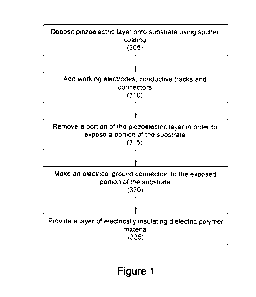
Figure 1 is a flowchart showing a method of producing an ultrasonic
transducer;
Figures 2 to 6 are schematic illustrations of examples of the steps of the
method of Figure 1,
wherein:
Figure 2 is a schematic of a step of depositing a piezoelectric layer onto a
conducting planar
substrate;
Figure 3 is a schematic of a step of adding electrodes, conductive tracks and
connectors;
Figure 4 is a schematic of a step of etching away a portion of the layer of
piezoelectric
material from the substrate;
Figure 5 is a schematic showing the fixing of a ground connection;
Figure 6 is a schematic showing the provision of a dielectric layer;
Figure 7 is a schematic planar view of an example of a ultrasonic transducer
array that could
be produced using the method of Figures 1 to 6; and
Figure 8 is schematic side view of the transducer array of Figure 7.
DETAILED DESCRIPTION OF THE DRAWINGS
A process for producing an ultrasonic transducer 5 (see Figures 7 and 8) is
shown in Figures
1 to 6. Figure 1 shows a flowchart of the manufacturing process. Figures 2 to
6 illustrate the
steps in the manufacturing process. Figures 3A, 4A, 5A and 6A show a side
cross sectional
view of the part that will become the ultrasonic transducer 5 and Figures 3B,
4B, 5B and 6B
show a planar view.
As indicated in step 305 of Figure 1 and as shown in Figure 2, a substrate 10
in the form of a
metal foil, such as aluminium foil is sputter coated on one side with a thin
layer of
polycrystalline piezoelectric material 15, such as transition metal doped
metal oxide. In this
example, the piezoelectric material is a vanadium doped zinc oxide (ZnO) or
aluminium
nitride (AIN), but other transition metal dopants or other metal salts
exhibiting piezoelectric
CA 03092312 2020-08-26
WO 2019/166805
PCT/GB2019/050549
properties could be used. The substrate can be from 20 to 200pm thick. The
layer of
piezoelectric material 15 is of the order of a 10th of the thickness of the
substrate 10, e.g.
from 2 to 20pm thick.
5 -- Beneficially, the layer of piezoelectric material 15 is deposited onto
the substrate 10 by
sputter coating. For example, the piezoelectric material 15 could be deposited
using a
magnetron based sputtering, such as closed field magnetron sputtering or high
power
impulse magnetron sputtering, which may optimize the piezoelectric properties
of the film
and/or the growth morphology.
In an example shown in Figure 2, the coating of the piezoelectric material 15
onto the
substrate 10 is performed using high power impulse magnetron sputtering (HI
PIMS), but the
invention is not limited to this. As shown in Figure 2, sputter coating is
generally performed
in a low pressure chamber 405 having an outlet 410 to a vacuum pump, an inlet
415 for
-- allowing inert gasses to be admitted, an electrode 420, a counter electrode
425 in the form
of a rotating drum, a target 430 electrically connected to the electrode 420,
and the substrate
10 being provided on a surface of the rotating drum counter electrode 425. A
grounded
magnetron anode 431 is provided proximate the target 430. A pulsed high
voltage power
supply (not shown) is connected to the electrode 420 that is coupled to the
target 430.
A separate substrate bias voltage power supply 432 is electrically connected
to the rotating
drum electrode 425 and operable to provide DC or RF biasing to the substrate
10. An
electric field is generated to guide ionized sputtered material from the
target 430 onto the
substrate 10. The substrate bias voltage can be varied or selected in order to
attract ionized
-- sputtered material from the target 430 to the substrate 10 to control the
energy of the arriving
ions. This may optimise sputter plasma ion energy during film growth. The drum
425 would
normally float electrically and the substrate bias voltage from the substrate
bias voltage
power supply 432 is applied through a rotational feedthrough / shaft of the
rotating drum 425,
thereby applying a voltage (bias) direct to the drum 425.
The target 430 is formed from the transition metal doped piezoelectric
material, e.g. from
vanadium doped zinc oxide. Importantly, the elements that will form the
layer of
piezoelectric material are combined within the target, e.g. by being alloyed
or doped, rather
-- than being provided separately or discretely, e.g. as mixtures or by the
doping transition
metals being adhered or otherwise provided on the surface of the metal oxide.
In this way,
the resultant layer of piezoelectric material 15 may have improved
piezoelectric properties.
CA 03092312 2020-08-26
WO 2019/166805
PCT/GB2019/050549
16
Furthermore, the rate of deposition may be increased, allowing shorter
deposition times
and/or thicker growth of the layer of piezoelectric material in a given time.
In addition, fewer
pinholes and other defects may occur.
The target 430 and the layer of piezoelectric material 15 have levels of the
active
piezoelectric material, e.g. the metal oxide or nitride such as the ZnO or
AIN, of 90% w/w
and above, e.g. from 90% to 99.99% w/w. The dopant/alloying material, e.g. the
transition
metal, is present in the target 420 and the layer of piezoelectric material 15
in levels of 10%
w/w and less, e.g. from 0.01% to 10% w/w.
A high voltage is provided between the electrode 420 and the counter electrode
425 that
acts to form a plasma in the chamber. Ions from the plasma are accelerated
into the target
430, sputtering the doped piezoelectric material from the target 430, which is
then deposited
on the surface of the substrate 10 by a process of adsorption. The result of
this is the
substrate 10 being coated on one side with the layer of transition metal doped
piezoelectric
material 15.
In step 310 and as shown in Figures 3A and 3B, the plurality of working
electrodes 20
respectively connected by corresponding conductive tracks 25 to corresponding
electrical
connectors 30 are provided on a surface of the layer of piezoelectric material
15 that is
opposite to the substrate 10. These may be provided by techniques such as
photo-masking
and deposition, printing, selective patterning, and/or the like.
In step 315 and as shown in Figures 4A and 4B, a portion of the layer of
piezoelectric
material 15 is removed to expose a corresponding portion of a surface of the
substrate 10
upon which the layer of piezoelectric material 15 is disposed. The portion of
piezoelectric
material 15 may be removed by selective etching, e.g. using an acid such as
hydrochloric
acid.
As indicated in step 320 and as shown in Figures 5A and 5B the electrical
ground
connection 17 is directly attached to this exposed portion of the surface of
the substrate 10
upon which the layer of piezoelectric material 15 is disposed. In this way,
all of the electrical
connections of the substrate 10 (i.e. the ground connection 17 and the
connection to the
layer of piezoelectric material 15 and thereby to the working electrodes 20)
are to the same
surface of the substrate 10 and no connections are directly made to the
opposite surface of
the substrate (i.e. the radiating surface from which the ultrasonic waves are
radiated in use).
With this construction, no folding of the material is required, which may
otherwise provide a
CA 03092312 2020-08-26
WO 2019/166805
PCT/GB2019/050549
17
point of potential failure. Furthermore, there is no damage or unwanted
modification of the
radiating surface of the substrate 10, such that the radiating surface is not
compromised.
In step 325 of Figure 1 and as shown in Figures 6A and 6B, the electrically
insulating
dielectric material 35 is provided over and around the outer surface of the
layer of
piezoelectric material 15 (i.e. the surface that is opposite to the surface
that abuts the
substrate 10), the electrodes 20 and the conductive tracks 25 in order to
protect and insulate
them. The dielectric material 35 is also disposed between the electrodes 20
and between
the conductive tracks 25. The dielectric material 35 can be any suitable
dielectric polymer
material, such as an epoxy, a polyimide, a poly para-xylene, or the like.
However, the
contacts 30 and the ground connection 17 are left exposed so that they can
form the
required electrical connections.
The dielectric material 35 is generally thinner than the substrate, e.g. being
50 microns or
less in thickness. The dielectric material 35 can be applied by suitable
techniques known in
the art such as by spin coating or by vapour deposition.
The above provision of the dielectric material 35 may confer advantages in the
ultrasonic
transducer array 5. For example, the operational frequency may be lowered or
high
frequency vibrations (e.g. those greater than 20MHz) may be damped, which is
particularly
beneficial in low frequency applications (e.g. in the range from 1 to 20MHz).
Furthermore,
the electrical insulation it provides may reduce pinhole and other defect
failures. It may also
help the transducer array 5 withstand higher voltage pulsing and improve
electrical durability.
It may also improve mechanical durability and recue failure due to curving and
flexing.
Figure 7 shows a schematic planar view of an exemplary ultrasonic transducer
array 5 that
could be produced using the method of claims 1 to 6 and Figure 8 shows a
schematic side
view of the ultrasonic transducer array 5. The ultrasonic transducer 5 shown
in Figures 7
and 8 is provided only as an example of an ultrasonic transducer that can be
produced using
the method of Figures 1 to 6 and the method could also be applied to produce
other
ultrasonic transducers and transducer arrays.
The exemplary ultrasonic transducer array 5 comprises the electrically
conductive substrate
10 in the form of a metal foil, in this case an aluminium foil, and the layer
of crystalline
piezoelectric material 15 disposed on one planar surface of the substrate 10.
The substrate
10 acts to support the layer of piezoelectric material 15 and also functions
as a ground
electrode. A surface of the substrate 10 that is opposite to a surface upon
which the layer of
CA 03092312 2020-08-26
WO 2019/166805
PCT/GB2019/050549
18
piezoelectric material is provided acts as an ultrasonic wave radiation
surface from which
ultrasonic waves are emitted from the transducer array in use. A portion of
the surface of
the substrate 10 that contacts the layer of piezoelectric material 15 is free
of piezoelectric
material and instead provided with an electrical ground connection 17.
The substrate 10 is much thicker (i.e. in the order of magnitude of 10 times
thicker) than the
layer of piezoelectric material 15 and in this example, the substrate 10 is
between 20 and
200pm thick and the layer of piezoelectric material 15 is between 2 and 20pm
thick. In this
example, the piezoelectric material is vanadium doped ZnO but it will be
appreciated that
other suitable piezoelectric materials such as AIN and/or other dopants,
particularly other
transition metal dopants, could be used.
One or more working electrodes 20 are provided on a surface of the layer of
piezoelectric
material 15 that is on an opposite side of the layer of piezoelectric material
15 to the
substrate 10. Each of the working electrodes 20 is connected to a
corresponding electrically
conductive track 25 that is in turn electrically connected to an associated
electrical connector
30.
A layer of electrically insulating dielectric polymer material 35 is provided
on the layer
piezoelectric material and over and in between the electrodes 20 and the
conductive tracks
25. Examples of suitable electrically insulating dielectric polymer material
35 include epoxy,
polyimide, poly para-xylene, or the like. However, the connectors 30 and the
connection of
the substrate 10 to electrical ground are left exposed to allow electrical
connections to a
controller or processing device to be made. The radiating surface of the
substrate 10 (i.e.
the surface of the substrate opposite to the piezoelectric material 15) is
also left exposed
and clear of encapsulation material. The thickness of the layer of dielectric
material 35 is in
the range from 1 to 50 microns thick.
In order to generate the ultrasound, an alternating electrical driving current
is applied to the
appropriate connector 30 or connectors 30 and thereby via the conductive
tracks 25 to the
corresponding working electrode 20 or electrodes 20. The working electrodes 20
form a
couple with the conductive substrate 10 that acts as a ground electrode (by
virtue of the
ground connection 17) in order to apply an alternating electrical current
across the
corresponding sections of the piezoelectric material 15.
This in turn causes the
corresponding sections of layer of piezoelectric material 15 to vibrate at
high frequency
along with the corresponding portion of the substrate 10 to thereby generate
ultrasonic
CA 03092312 2020-08-26
WO 2019/166805
PCT/GB2019/050549
19
waves, which are emitted from portions of the outer surface of the substrate
10 that
correspond to the driven working electrode(s) 20.
Although specific examples are described above in relation to the Figures, it
will be
appreciated that variations on the above examples are possible. As such, the
scope of
protection is defined by the claims and not by the above specific examples.
For example, although examples of piezoelectric materials being ZnO or AIN are
given
above, it will be appreciated that other piezoelectric materials could be used
instead.
Furthermore, although transition metal doped piezoelectric materials are
described, it will be
appreciated that non-doped piezoelectric materials could be used. In addition,
although
various thicknesses, dimensions, numbers and geometric arrangements of
electrodes,
conductive tracks and contacts are given above, it will be appreciated that
other thicknesses,
dimensions, numbers and geometric arrangements of electrodes, conductive
tracks and
contacts could be used. Indeed, although the electrodes are all shown as the
same size and
shape, it will be appreciated that at least some or all of the electrodes may
be of different
sizes and/or shapes. Although various specific examples of dielectric
materials are given,
other suitable dielectrics could be used. Although specific examples of
etching agents are
used, other suitable etching agents could alternatively be used.
Furthermore, although the example given above beneficially uses sputter
coating of a
transition metal doped metal oxide or metal nitride using a doped, alloyed or
amalgam
target, it will be appreciated that other methods of producing a suitably
integral transition
metal / metal oxide or metal nitride piezoelectric could be used. For example,
the transition
metal and the metal oxide or metal nitride could be co-deposited from a dual
source system.
In addition, although the substrate 10 is shown in Figure 2 on a rotating drum
whilst the
piezoelectric layer 15 is deposited onto the substrate 10, it will be
appreciated that the
substrate 10 may be provided on a flat, stationary surface.