Note : Les descriptions sont présentées dans la langue officielle dans laquelle elles ont été soumises.
CA 03094156 2020-09-16
METHOD FOR PROCESSING ELECTRONIC AND ELECTRICAL DEVICE
COMPONENT SCRAP
FIELD OF THE INVENTION
[0001]
The present invention relates to a method for processing electronic and
electrical device component scrap. More particularly, it relates to a method
for
processing electronic and electrical device component scrap, which is suitable
for
recycling of used electronic and electrical devices.
BACKGROUND OF THE INVENTION
[0002]
From the viewpoint of recent resource conservation, recovery of variable
metals from electronic and electrical device component scrap such as waste
electronic home appliances, PCs and mobile phones has increasingly become
popular, and an efficient method for recovering the valuable metals has been
studied and proposed.
[0003]
For example, Japanese Patent Application Publication No. H09-78151 A
(Patent Literature 1) discloses a recycling method for valuable metals,
including the
steps of charging scrap containing valuable metals into a flash furnace for
smelting
copper ores, and recovering the valuable metals into a mat that is retained in
the
furnace. According to such a recycling method, scrap processing can be
combined
with copper smelting in the copper smelting flash furnace, so that the
valuable
metals can be recovered at low cost even from scrap having a lower content of
the
valuable metals.
[0004]
- 1 -
CA 03094156 2020-09-16
However, in the processing using the copper smelting flash furnace as
disclosed in Patent Literature 1, an increased amount of the electronic and
electrical
device component scrap processed may lead to an increase in a carbon component
contained in organic substances such as resins forming the electronic and
electrical
device component scrap, which may cause troubles due to over-reduction in the
smelting furnace. On the other hand, since the amount of the electronic and
electrical device component scrap processed tends to be increased in recent
years,
there is a need for efficient processing in the copper smelting flash furnace.
[0005]
As one of methods for suppressing the generation of troubles due to over-
reduction in the copper smelting flash furnace, it is proposed that the
electronic and
electrical device component scrap is crushed before processing of the
electronic
and electrical device component scrap in a copper smelting flash furnace to
reduce
the volume. For example, Japanese Patent Application Publication No. 2015-
123418 A (Patent Literature 2) discloses that electrical and electronic device
component scrap containing copper is incinerated and then crushed to have a
predetermined size or less, and the crushed electrical and electronic device
component scrap is processed in a copper smelting furnace.
[0006]
However, the increased amount of electronic and electrical device
component scrap processed leads to introduction of a larger amount of unwanted
substances (smelting inhibitors) for processing in the subsequent copper
smelting
step than that of the prior arts, depending on types of substances contained
in the
electronic and electrical device component scrap. An increased amount of such
smelting inhibitors introduced into the copper smelting step arises a
situation where
an amount of the electronic and electrical device component scrap to be
introduced
has to be limited.
- 2 -
CA 03094156 2020-09-16
[0007]
Conventionally, many efforts have been made for thermodynamic methods in
a smelting step and purifying methods for electrolytic solutions in an
electrolytic step
of copper smelting, including the smelting inhibitors derived from natural
ores.
However, there are many problems in the method for processing the electronic
and
electrical device component scrap having very high contents of the smelting
inhibitors than the natural ores.
CITATION LIST
Patent Literatures
[0008]
[Patent Literature 1] Japanese Patent Application Publication No. H09-78151 A
[Patent Literature 2] Japanese Patent Application Publication No. 2015-123418
A
SUMMARY OF THE INVENTION
Technical Problem
[0009]
In view of the above problems, the present invention provides a method for
processing electronic and electrical device component scrap, which can
increase an
amount of electronic and electrical device component scrap processed in a
smelting
step and efficiently recover valuable metals.
Solution to Problem
[0010]
As a result of intensive studies to solve the above problems, the present
inventors have found that it is effective to subject electronic and electrical
device
component scrap to sorting processes in certain order, as a processing method
that
- 3 -
CA 03094156 2020-09-16
can minimize smelting inhibitors contained in the electronic and electrical
device
component scrap, which would otherwise be carried into the smelting step.
[0011]
In one aspect, the present invention completed on the basis of the above
findings provide a method for processing electronic and electrical device
component
scrap, the method comprising: a step 1 of removing powdery materials and film-
shaped component scrap from the electronic and electrical device component
scrap;
a step 2 of concentrating synthetic resins and substrates from the electronic
and
electrical device component scrap from which the powdery materials and film-
shaped component scrap have been removed; and a step 3 of concentrating the
substrates containing valuable metals from a concentrate obtained in the step
2.
[0012]
In one embodiment, the method for processing electronic and electrical
device component scrap according to the present invention further comprises,
prior
to the step 1, a pre-processing step A of removing wire scrap contained in the
electronic and electrical device component scrap.
[0013]
In another embodiment, the method for processing electronic and electrical
device component scrap according to the present invention further comprises a
step
B of removing wire scrap contained in the electronic and electrical device
component scrap between the steps 1 and 2.
[0014]
In another embodiment, the method for processing electronic and electrical
device component scrap according to the present invention further comprises,
prior
to the step 3, a step C for decreasing a metal content in the concentrate
obtained in
the step 2.
[0015]
- 4 -
CA 03094156 2020-09-16
In still another embodiment of the method for processing electronic and
electrical device component scrap according to the present invention, the step
1 is
wind force sorting.
[0016]
In still another embodiment of the method for processing electronic and
electrical device component scrap according to the present invention, the step
2 is
wind force sorting.
[0017]
In still another embodiment of the method for processing electronic and
electrical device component scrap according to the present invention, the step
3
comprises processing the substrates with a sorter, the sorter comprising: a
metal
sensor; a color camera; an air valve; and a conveyor.
[0018]
In still another embodiment of the method for processing electronic and
electrical device component scrap according to the present invention, the step
B
comprises removing the wire scrap using a sieving machine having a slit-shaped
sieve.
[0019]
In still another embodiment of the method for processing electronic and
electrical device component scrap according to the present invention, the step
C
comprises at least one process selected from sorting with a color sorter,
sorting with
sieving, and sorting with magnetic sorting.
Advantageous Effects of Invention
[0020]
According to the present invention, it is possible to provide a method for
processing electronic and electrical device component scrap, which can
increase an
- 5 -
CA 03094156 2020-09-16
amount of electronic and electrical device component scrap processed in a
smelting
step and efficiently recover valuable metals.
BRIEF DESCRIPTION OF THE DRAWINGS
[0021]
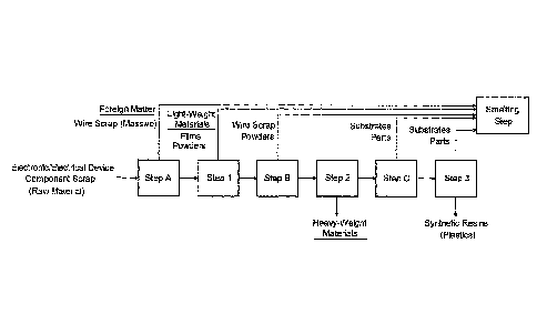
FIG. 1 is a processing flow chart illustrating an example of a processing flow
of electronic and electrical device component scrap according to an embodiment
of
the present invention.
DETAILED DESCRIPTION OF THE INVENTION
[0022]
An embodiment of the present invention will be described below with
reference to the processing flow chart of FIG. 1. The method for processing
electronic and electrical device component scrap according to the embodiment
of
the present invention includes at least a step 1, a step 2, and a step 3.
Further,
steps A to C can be optionally combined before and after the steps 1 to 3
according
to properties of the electronic and electrical device component scrap.
[0023]
As used herein, the "electronic and electrical device component scrap" refers
to scrap obtained by crushing electronic and electrical devices such as waste
home
electric appliances, PCs, and mobile phones, recovering them and then crushing
them to have an appropriate size. In the present invention, the crushing for
obtaining the electronic and electrical device component scrap may be
performed by
an operator. However, crushed objects may be purchased on the market.
[0024]
The crushing method is carried out by any apparatus that is not limited to a
specific apparatus, and may be carried out in sharing or shock manner. It is
- 6 -
CA 03094156 2020-09-16
desirable to carry out crushing such that the shape of the component is
maintained
as much as possible. Therefore, the apparatus does not include one belonging
to
the category of a crusher for the purpose of fine crashing.
[0025]
The electronic and electrical device component scrap according to the
present embodiment can be classified into component scrap consisting of
synthetic
resins (plastics) used for substrates, parts such as ICs and connectors, and
casings;
wire scraps; metals; film-shaped component scrap; powders generated by
crushing
or pulverizing; and others, and they can be further classified into subclasses
depending on purposes of the processing. In the present embodiment, the
electronic and electrical device component scrap that has been crushed to have
a
particle diameter of 50 mm or less and has a percentage of individual
components
separated as component scrap of 70% or more may preferably be processed,
although not limited thereto.
[0026]
(1) Step 1
In the step 1, powdery materials and film-shaped component scrap (resins,
aluminum foils, and the like) as materials that would be adversely affected on
the
subsequent sorting step are selectively removed from the raw material
electronic
and electrical device component scrap. This serves as pre-processing for the
subsequent step and is categorized as coarse sorting.
[0027]
As the step 1, wind force sorting is preferably used. For the purpose of the
present invention, this wind force sorting is characterized by an ability to
process a
large number of materials. By the wind force sorting, the materials were
divided
into light-weight materials and heavy-weight materials. The powdery materials
and
film-shaped scrap (resins, aluminum foils, and the like) as the light- weight
materials
- 7 -
CA 03094156 2020-09-16
are sent to a copper smelting step via a pre-incineration processing step, and
the
heavy-weight materials are sent to the step 2.
[0028]
A flow rate of air in the step 1 can be set to 5 to 20 m/s, and more
preferably
to 12 m/s, and further preferably about 5 to 10 m/s, and even more preferably
6 to
8 m/s, although not limited to those conditions.
[0029]
(2) Step 2
In step 2, synthetic resins, substrates and parts are concentrated from the
electronic and electrical device component scrap from which the powdery
materials
and film-shaped component step has been removed.
[0030]
As the step 2, wind force sorting is preferably used. In the step 2, massive
metals or other individual components are separated as heavy-weight materials,
and
substrates, plastics and other synthetic resins are concentrated on the light-
weight
material side. The substrates and synthetic resins concentrated on the light-
weight
material side are sent to the step 3 that is the next step. Further, the heavy-
weight
materials are optionally subjected to a combination of magnetic force sorting,
eddy
current sorting, color sorter, manual sorting, robot sorting, and the like to
recover
metals such as Fe, Al and SUS which are present in the heavy-weight materials.
[0031]
A flow rate of air in the step 2 can be set to 5 to 20 m/s, more preferably 10
to
18 m/s, further preferably 15 to 18 m/s, and even more preferably about 16 to
17
m/s, although not limited to those conditions.
[0032]
(3) Step 3
- 8 -
CA 03094156 2020-09-16
In the step 3, substrates containing valuable metals such as copper, gold,
and silver are concentrated from the light-weight materials containing the
substrates,
the synthetic resins, and the like obtained in the step 2. By concentrating
the
substrates containing the valuable metals and processing them in a copper
smelting
step as described later, a recovery efficiency of the valuable metals in the
copper
smelting step can be improved.
[0033]
In the step 3, the processing is preferably carried out using a sorter
including
a metal sensor, a color camera, an air valve and a conveyor. In the step 3,
first,
the metal sensor detects the metals, the conveyer conveys and discharges the
metals, and the subsequent color camera confirms positions of the substances.
Then, based on information from the metal sensor and positional information
from
the color camera, it is preferable to carry out a process of selectively
shooting down
the components which are recognized as non-metal objects and are on a falling
trajectory, by means of the air valve.
[0034]
The substrates containing the valuable metals such as copper and precious
metals are concentrated on the side of the sorted products that have not been
shot
down by the air valve. Therefore, those substrates can be used as processing
objects to increase an efficiency of recovering valuable metals with a less
amount of
component scrap introduced.
[0035]
On the other hand, the substrates and the synthetic resins that are
substantially free of metal, shot down by the air valve, may contain Sb or one
or
more metals selected from the group consisting of Sb, Al, Fe and Ni, which
will be
smelting inhibitors in a smelting step as described later. By sending the
component
scrap containing such smelting inhibitors to the smelting step, it may be
difficult to
- 9 -
CA 03094156 2020-09-16
perform the smelting step stably, so that it may be difficult to recover the
valuable
metals with a high efficiency.
[0036]
According to the processing method of the present embodiment, by the step
3, the substrate scrap and the like containing at least Sb or one or more
metals
selected from the group consisting of Sb, Al, Fe, and Ni which are the
smelting
inhibitors can be removed in advance, thereby preventing the smelting
inhibitors
contained in the electronic and electrical device component from being brought
as
much as possible.
[0037]
In addition, when the powdery materials or the film-shaped component scrap
are contaminated into the processing objects in the process of the step 3, the
metal
sorter results in deterioration of the field of view of the color camera by
flowing up
the powdery materials and the like during the sorting, so that it may be
difficult to
specify the removing objects using the color camera, or the color camera may
erroneously detect the removing objects and the air valve may be erroneously
operated to cause non-objects to be caught into the valve.
[0038]
According to the method according to the embodiment of the present
invention, the powdery materials, the film-shaped component scrap and the like
contained in the electronic and electrical device component scrap, which
causes a
decrease in the sorting efficiency in the sorting step, have been previously
removed
in the step 1 and the step B, so that it is possible to suppress malfunction
of the
metal sorter and the decrease in the sorting efficiency due to flowing-up of
the
powdery materials during the processing.
[0039]
- 10 -
CA 03094156 2020-09-16
In a general physical sorting method for concentrating metals, the metals are
first recovered by magnetic force sorting or the like. However, the magnetic
force
sorter has a risk that the component scrap containing the valuable metals may
be
contaminated into the magnetic material to decrease an amount of the valuable
metals recovered.
[0040]
According to the processing method according to the embodiment of the
present invention, the wind force sorting is carried out in two stages (the
step 1 and
the step 2) in the initial stage of physical sorting, so that a large amount
of electronic
and electrical device component scrap (raw materials) can be sorted at once
while
concentrating a larger amount of valuable metals than the case where the
process
of the magnetic force sorting is carried out. Then, after the two-stage wind
power
sorting, the sorting process (step 3) using the metal sorter, which requires a
long
processing time, can be combined, thereby removing the smelting inhibitors
while
increasing the amount of the electronic and electrical device component scrap
to
recover the valuable metals efficiently.
[0041]
As shown in FIG. 1, it is more preferable to combine the steps A to C before
and after the steps 1 to 3 in terms of an improved sorting efficiency. It is
preferable
that the step A is a pre-processing step of removing the wire scrap contained
in the
electronic and electrical device component scrap, prior to the step 1. For
example,
depending on the type of the electronic and electrical device component scrap,
a
large amount of scrap may be contained so that the scrap can be easily
identified by
visual inspection. Therefore, it is preferable to remove the wire scrap by
manual
sorting or mechanical sorting using a robot or the like, prior to the step 1.
[0042]
- 11 -
CA 03094156 2020-09-16
It is preferable to have the step B of removing the wire scrap contained in
the
electronic and electrical device component scrap between the step 1 and the
step 2.
As the step B, the wire scrap is preferably removed using a sieving machine
having
a slit-shaped sieve. In the step B, the powdery materials can be removed in
addition to the wire scrap by sieving. The sieved powdery materials and copper
wire scrap can be sent to the smelting step via the pre-incineration
processing step
to recover the valuable metals in the component scrap more efficiently.
[0043]
A step C may be carried out between the step 2 and the step 3. The step C
includes at least one process of sorting with a color sorter, sorting with
sieving, and
sorting with magnetic sorting, and can be regarded as a pre-processing for the
sorting process of the step 3. These sorting processes can be combined to
decrease the metal content in the processing objects sent to the step 3.
[0044]
A higher metal content in the processing objects means that there is a large
amount of component scrap containing the metals. In the process using the
metal
sorter in the step 3, when there are non-metal objects such as synthetic
resins
between the component scraps detected as the metals, they may be erroneously
detected as a single metal when a distance between the component scraps is
within
a detection range of the metal sensor, and the synthetic resins such as
plastics,
which are non-metal objects between the metal objects, may not repelled by the
air
valve and handled as metal-containing substrates. Therefore, before carrying
out
the separation using the metal sorter in the step 3, the step C including the
sorting
with the magnetic sorting, the sieving, the color sorter, and the like can be
carried
out to decrease the metal content in the processing objects sent to the step 3
to
suppress the erroneous detection of the metal sorter.
[0045]
- 12 -
CA 03094156 2020-09-16
A part of the substrate scrap to be processed in the copper smelting step
may be contaminated into the heavy-weight materials obtained in the step 2.
Therefore, the heavy-weight materials obtained in step 2 are further
classified by a
process such as magnetic force sorting, eddy current sorting, color sorter,
manual
sorting, and robot sorting, thereby separating the substrate scrap to be
processed in
the copper smelting process to send them to the smelting the step. Therefore,
the
recovery efficiency of the valuable metals can be improved.
[0046]
In addition, the "removed" or "separated" as used herein includes not only an
embodiment of removal or separation of 100%, but also an embodiment of removal
of 30% or more, more preferably 50% by mass or more in the weight ratio in the
objects.
[0047]
- Smelting Step ¨
A method for processing electronic and electrical device component scrap
according to an embodiment of the present invention includes a smelting step
of
processing electronic and electrical device component scrap containing
valuable
metals sorted in each of the steps 1 to 3 and the step A to C, in the smelting
step.
[0048]
When recovering copper as a valuable metal, the smelting step is carried out
using a smelting furnace. The smelting step includes: a step of incinerating
the
electronic and electrical device component scrap; a step of crushing and
sieving the
incinerated scrap; and a step of subjecting the crushed and sieved scrap to
copper
smelting. The step of processing the electronic and electrical device
component
scrap is preferably carried out prior to the incinerating step.
[0049]
- 13 -
CA 03094156 2020-09-16
As the smelting step according to the present embodiment, a copper smelting
step using a flash furnace method can be preferably employed, although not
limited
thereto. In the copper smelting step using the flash furnace method, for
example,
copper concentrates, a solvent, and the electronic and electrical device
component
scrap are charged from a ceiling portion of a shaft of the flash furnace. The
charged concentrates and the electronic and electrical device component scrap
are
melted in the shaft of the flash furnace to separate a mat containing, for
example,
from 50 to 68% of copper and slag floating above the mat in a settler of the
flash
furnace. Valuable metals such as copper, gold, and silver in the electronic
and
electrical device component scrap are absorbed into the mat that is retained
in the
flash furnace, so that the valuable metals can be recovered from the
electronic and
electrical device component scrap.
[0050]
In copper smelting, it is important to introduce the electronic and electrical
device component scrap having lager contents of valuable metals such as
copper,
gold and silver as the raw material to be processed, as much as possible, and
carry
out the processing, in order to produce copper and recover larger amounts of
variable metals such as gold and silver. On the other hand, the electronic and
electrical device component scrap contains substances that would affect the
quality
of products and byproducts in copper smelting and/or smelting inhibitors that
would
affect the copper smelting process. For example, the introduction of an
increased
amount of substances containing elements such as Sb and Ni as described above
may lead to deterioration of the quality of electrolytic copper obtained by
copper
smelting.
[0051]
Further, in a non-ferrous metal smelting step such as copper smelting,
sulfuric acid is produced from sulfur dioxide generated by oxidation of
concentrates.
- 14 -
CA 03094156 2020-09-16
However, when hydrocarbon is mixed into sulfur dioxide, the produced sulfuric
acid
may be colored. Examples of sources of hydrocarbons include synthetic resins
such as plastics, and a large amount of such synthetic resins may be contained
depending on the composition of the electronic and electrical device component
scrap carried into the copper smelting. The synthetic resins may also cause
rapid
combustion and smoke leakage in the smelting furnace, and even deterioration
of
equipment due to local heating.
[0052]
Furthermore, for example, the presence of Al, Fe, or the like over a certain
concentration in the smelting furnace may lead to a change of a slag
composition in
the process of copper smelting, which may affect the loss of valuable metals
into the
slag, so-called slag loss. Moreover, a large amount of halogen elements such
as
Cl, Br, and F contained in the electronic and electrical device component
scrap to be
introduced into the smelting furnace may cause corrosion of exhaust gas
treatment
equipment for copper smelting and deterioration of a sulfuric acid catalyst.
Such a
problem of contamination of the smelting inhibitors becomes apparent as an
amount
of the electronic and electrical device component scrap processed is
increased,
which cases a problem that the smelting step is burdened.
[0053]
The method for processing the electronic and electrical device component
scrap according to an embodiment of the present invention includes, prior to
the
smelting step, a physical sorting step of the electronic and electrical device
component scrap, as shown in FIG. 1. This can allow a proportion of smelting
inhibitors that are carried into the smelting step to be minimized, and allow
an
amount of the electronic and electrical device component scrap processed to be
increased, and allow the proportion of the electronic and electrical device
- 15 -
CA 03094156 2020-09-16
component scrap containing copper and valuable metals to be increased to
recover
copper and valuable metals efficiently.
[0054]
It is more preferable that a larger amount of the smelting inhibitors
contained
in the electronic and electrical device component scrap is removed. However,
there is component scrap having the smelting inhibitors and the valuable
metals at
the same time, depending on the type of the component scrap. By removing 1/2,
more preferably 2/3 or more, in a weight ratio, of the smelting inhibitors in
the entire
electronic and electrical device component scrap raw material, the electronic
and
electrical device component scrap can be stably processed in the copper
smelting
step. Furthermore, assuming that a limit amount that can process the smelting
inhibitors is the same as the present limit in the smelting process, the
smelting
inhibitors in the entire electronic and electrical device component scrap raw
material
are decreased, whereby a larger amount of electronic and electrical device
component scrap containing a decreased amount of the smelting inhibitors can
be
processed in the smelting step.
[0055]
According to the method for processing the electronic and electrical device
component scrap according to the embodiment of the present invention, it is
possible to provide a method for processing electronic and electrical device
component scrap, which includes a physical sorting step of sorting and
removing
component scrap containing smelting inhibitors for each unit of components in
the
state of the component scrap before crushing the electronic and electrical
device
component scrap into powder in the smelting step, whereby a processing amount
of
the electronic and electrical device component scrap to be processed in the
smelting
process can be increased, and valuable metals can be efficiently recovered.
- 16 -