Note : Les descriptions sont présentées dans la langue officielle dans laquelle elles ont été soumises.
CA 03100449 2020-11-16
PTS-0007-CA
RADIOFREQUENCY MODULE
Technical field
[0001] The present invention relates to a radiofrequency (RF) module
intended to
form the passive part of a direct radiating antenna (DRA, Direct Radiating
Array).
Prior art
[0002] Antennas are elements that serve to transmit electromagnetic
signals in
free space, or to receive such signals. Simple antennas, such as dipoles, have
limited
performance in terms of gain and directivity. Parabolic antennas provide
higher
directivity, but are bulky and heavy, making their use inappropriate in
applications
such as satellites, for example, where weight and volume need to be reduced.
[0003] Also known are antenna arrays (DRA) which combine a plurality of
phase-
shifted radiating elements (elementary antennas) in order to improve gain and
directivity. The signals received on the different radiating elements, or
transmitted by
these elements, are amplified with variable gains and phase-shifted from one
another
in order to control the shape of the reception and transmission lobes of the
array.
[0004] At high frequency, for example at microwave frequencies, each of
the
different radiating elements is connected to a waveguide which transmits the
received
signal toward electronic radiofrequency modules, or which supplies this
radiating
element with a radiofrequency signal to be transmitted. The signals
transmitted or
received by each radiating element may also be separated according to their
polarization, using a polarizer.
[0005] The assembly formed by the radiating elements (elementary antennas)
in
an array, the associated waveguides, any filters that are used, and the
polarizers is
referred to in the present text as a passive radiofrequency module. The
waveguides
and the associated polarizers are referred to as a feed unit (" feed network
"). The
assembly is intended to form the passive part of a direct radiating array
(DRA).
Date Recue/Date Received 2020-11-16
CA 03100449 2020-11-16
2 PTS-0007-
CA
[0006] Arrays of radiating elements for high frequencies, notably
microwave
frequencies, are difficult to design. In particular, it is often desirable to
place the
different radiating elements of the array as closely together as possible, in
order to
reduce the amplitude of the secondary transmission or reception lobes in
directions
other than the transmission or reception direction which is to be given
priority.
However, this reduction of the spacing between the different radiating
elements of the
array is incompatible with the minimum size required by the polarizers, on the
one
hand, and with the overall dimensions of the electronic amplification and
phase-
shifting circuits upstream of the polarizers on the other hand.
[0007] Therefore the size of the polarizers and the electronic system
usually
determines the minimum spacing between the different radiating elements of an
array. The resulting wide spacing gives rise to undesirable secondary
transmission or
reception lobes.
[0008] However, other radiofrequency modules require a wider spacing of
the
radiating elements, in order to provide them with a transmission cone, for
example. It
may also be desirable to modify the relative positioning of the radiating
elements.
Brief description of the invention
[0009] An object of the present invention is therefore to propose a
passive
radiofrequency module, intended to form the passive part of a direct radiating
array
(DRA), which is free of, or minimizes, the limitations of the known devices.
[0010] These aims are, notably, achieved by means of a radiofrequency
module
comprising:
a first layer comprising an array of radiating elements, each radiating
element having a cross section for supporting at least one wave propagation
mode,
a second layer forming an array of waveguides;
a fourth layer forming an array of ports;
the second layer being interposed between the first and the fourth
layer;
each waveguide being intended to transmit a radiofrequency signal in
Date Recue/Date Received 2020-11-16
CA 03100449 2020-11-16
3 PTS-0007-
CA
one or other direction between a port of the fourth layer and a radiating
element;
the surface area of the first layer being different from the surface area
of the fourth layer;
the waveguides approaching one another between the fourth layer and
.. the first layer, or between the first layer and the fourth layer.
[0011] These aims are, in particular, achieved by means of a
radiofrequency
module comprising:
a first layer comprising an array of radiating elements, each radiating
element having a cross section for supporting at least one wave propagation
mode,
each section being provided with at least one ridge parallel to the direction
of
propagation of the signal;
a second layer forming an array of waveguides;
a fourth layer forming an array of ports;
the second layer being interposed between the first and the fourth
layer;
each waveguide being intended to transmit a radiofrequency signal in
one or other direction between a port of the fourth layer and a radiating
element;
the surface area of the first layer being smaller than the surface area of
the fourth layer;
the waveguides approaching one another between the fourth layer and
the first layer.
[0012] Thus the waveguides have a double function; on the one hand, they
enable
the signals to be transmitted between the ports of the fourth layer and the
radiating
elements of the first layer, and on the other hand they enable the spacing of
the
radiating elements and the spacing of the ports of the fourth layer to be
chosen
independently.
[0013] In a first embodiment, the waveguides approach one another between
the
fourth layer and the first layer, in a converging manner. The surface area of
the first
layer is then smaller than the surface area of the fourth layer.
Date Recue/Date Received 2020-11-16
CA 03100449 2020-11-16
4 PTS-0007-
CA
[0014] Thus this arrangement enables the spacing between the radiating
elements
of the first layer to be reduced, in order to reduce the amplitude of the
undesirable
side lobes ("grating lobes").
[0015] For this purpose, the spacing (p1) between two radiating elements
of the
first layer is preferably less than X/2, X being the wavelength at the maximum
operating frequency.
[0016] The converging arrangement of the waveguides from the fourth layer
toward the radiating elements thus enables the ports of the fourth layer to be
spaced
apart. The wide spacing between the ports makes it possible, for example, to
position
the electronic amplification and phase-shifting circuit supplying each port in
the
immediate vicinity of each port, reducing the constraints on the dimensions of
this
circuit. This wide spacing also enables polarizers of sufficient size to be
positioned in
the proximity of each port if necessary, to provide effective separation of
the signals
according to their polarization.
[0017] In another embodiment, the surface area of the first layer is larger
than the
surface area of the fourth layer. The waveguides then become more distant from
one
another between the fourth layer and the first layer. This embodiment enables
relatively large radiating elements to be used, without requiring a large port
layer.
[0018] The arrangement of the radiating elements of the first layer may
be
different from the arrangement of the ports of the fourth layer. For example,
the
radiating elements of the first layer may be positioned in a rectangular
matrix MxN,
while the ports of the fourth layer are positioned in a rectangular matrix
KxL, M being
different from K and N being different from L. This different arrangement may
also
result in different shapes, for example a rectangular arrangement on one of
the layers
and a circular, oval, cross-shaped, hollow rectangle, polygonal, or other
arrangement
on the other layer.
[0019] The radiofrequency module may comprise a third layer interposed
between the second and the fourth layer.
Date Recue/Date Received 2020-11-16
CA 03100449 2020-11-16
PTS-0007-CA
[0020] The elements of the third layer may cause a transformation of the
signal.
[0021] The third layer may also comprise an array of elements providing a
cross
section adaptation between the output cross section of the ports of the fourth
layer
and the differently-shaped cross section of the waveguides. A third layer of
this type
5 may, notably, be provided when only the ports or only the waveguides are
ridged.
[0022] The third layer interposed between the second layer and the fourth
layer
may also comprise an array of polarizers as elements.
[0023] In a variant, the radiofrequency module may comprise external
polarizers
immediately after the radiating elements in the air.
[0024] The third layer interposed between the second and the fourth layer
may
comprise a filter.
[0025] Each radiating element of the first layer may be provided with at
least one
ridge parallel to the direction of propagation of the signal.
[0026] The radiating elements of the first layer may also be non-ridged
and may
consist of open waveguides or square, circular, pyramidal or spline-shaped
horns.
[0027] The radiating elements may have an external cross section which is
square,
rectangular, or preferably hexagonal, circular or oval.
[0028] The spacing (p1) between two radiating elements may be variable
within
the module.
[0029] The radiofrequency module may comprise waveguides having a square,
rectangular, round, oval or hexagonal cross section, the inner faces of which
are
provided with at least one ridge extending longitudinally along each inner
face of the
waveguides.
Date Recue/Date Received 2020-11-16
CA 03100449 2020-11-16
6 PTS-0007-
CA
[0030] Each waveguide of the second layer is preferably designed to
transmit
either a fundamental mode only, or a fundamental mode and a single degenerate
mode.
[0031] The lengths of the different waveguides of the second layer are
advantageously identical.
[0032] The lengths of the different waveguides of the second layer may
also be
variable; in this case, it is preferable to use waveguides that are isophase
at the
wavelength concerned, that is to say waveguides that all produce an identical
phase
shift.
[0033] In one embodiment, the different waveguides have different lengths
and
different cross sections, so as to compensate the phase variation produced by
the
different lengths. The different waveguides are preferably isophase; that is
to say, the
phase shifts across the different waveguides are identical.
[0034] The channels of different waveguides are preferably non-
rectilinear.
[0035] The waveguides of the second layer are preferably curved.
[0036] The curvature of the different waveguides of the second layer may
be
variable. For example, the waveguides at the periphery may be more curved than
the
waveguides in the center.
[0037] The ports of the fourth layer may form the inputs of a polarizer.
[0038] A first end of all the waveguides may be located in a first plane,
while a
second end of all the waveguides is located in a second plane.
[0039] The module is advantageously a module formed by additive
manufacturing.
Date Recue/Date Received 2020-11-16
CA 03100449 2020-11-16
7 PTS-0007-
CA
[0040] Additive manufacturing may be used, notably, to form waveguides
having a
complex shape, notably curved waveguides converging in funnel fashion between
the
layer of radiating elements and the layer of polarizers.
[0041] "Additive manufacturing" is taken to mean any method of
manufacturing
parts by the addition of material, according to computer data stored on a
computer
medium and defining a model of the part. In addition to stereolithography and
selective laser melting, the expression denotes other methods of manufacture
by the
setting or coagulation of liquid or powder, notably including, but not limited
to,
methods based on ink jets (binder jetting), DED (Direct Energy Deposition),
EBFF
(Electron beam freeform fabrication), FDM (fused deposition modeling), PFF
(plastic
freeforming), the use of aerosols, BPM (ballistic particle manufacturing),
powder bed,
SLS (Selective Laser Sintering), ALM (additive Layer Manufacturing), polyjet,
EBM
(electron beam melting), photopolymerization, etc. However, manufacturing by
stereolithography or selective laser melting is preferred, because it enables
parts to be
produced with relatively clean surface states having low roughness.
[0042] The module is preferably monolithic.
[0043] Monolithic manufacture of the module enables costs to be reduced,
while
avoiding the need for assembly. It also makes it possible to ensure the
precise relative
positioning of the different components.
[0044] The invention also relates to a module comprising the above elements
and
to an electronic circuit with amplifiers and/or phase shifters connected to
each port.
Brief description of the drawings
[0045] Examples of embodiment of the invention are indicated in the
description
illustrated by the appended drawings, in which:
= Figure 1 shows a schematic side view of the different layers of a module
according to the invention.
Date Regue/Date Received 2020-11-16
CA 03100449 2020-11-16
8 PTS-
0007-CA
= Figure 2 shows two examples of embodiment of the third layer, in which
each element of this layer comprises either one or two inputs on the side
facing the
fourth layer.
= Figure 3A shows a perspective view of the second and third layer of an
example of a module according to the invention.
= Figure 3B shows a front view of the second and third layer of an example
of
a module according to the invention, viewed from the third layer.
= Figure 3C shows a front view of the second and third layer of an example
of
a module according to the invention, viewed from the side corresponding to the
first
layer.
= Figure 4 shows a perspective view of an example of a first layer of a
module according to the invention.
= Figures 5A to 5C show three examples of radiating elements that may be
used in the first layer of a module according to the invention.
= Figure 6 shows a front view of another example of a first layer of a
module
according to a second embodiment of the invention.
= Figure 7 shows a perspective view of a module comprising a set of
waveguides converging toward the radiating elements of the first layer
according to a
third embodiment of the invention.
= Figure 8 shows a view from the fourth layer of the module according to
the
third embodiment of the invention.
= Figure 9 shows a side view of the module according to the third
embodiment of the invention.
Date Recue/Date Received 2020-11-16
CA 03100449 2020-11-16
9 PTS-0007-
CA
= Figure 10 shows another side view of the module according to the third
embodiment of the invention.
= Figure 11 shows a perspective view of a module comprising a set of
waveguides diverging toward the radiating elements of the first layer,
according to a
fourth embodiment of the invention.
= Figure 12 shows a side view of the module according to the fourth
embodiment of the invention.
Example(s) of embodiment of the invention
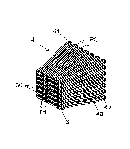
[0046] Figure 1 shows a passive radiofrequency module 1 according to a
first
embodiment of the invention, intended to form the passive part of a direct
radiating
array (DRA).
[0047] The radiofrequency module 1 comprises four layers 3, 4, 5, 6.
[0048] Of these layers, the first layer 3 comprises a two-dimensional
array of N
radiating elements 30 (antennas) for transmitting electromagnetic signals into
the
ether, or for receiving the received signals.
[0049] The second layer 4 comprises an array of waveguides 40.
[0050] The third layer 5 is optional; it may also be integrated into the
layer 4. If
present, the third layer 5 comprises an array of elements 50, for example
polarizers or
cross section adapters.
[0051] The fourth layer 6 comprises a two-dimensional array, for example
a
rectangular matrix, with N waveguide ports 60. Each port 60 forms an interface
with an
active element of the DRA such as an amplifier and/or a phase shifter, forming
part of
a beamforming array. Thus a port enables a waveguide to be connected to an
Date Recue/Date Received 2020-11-16
CA 03100449 2020-11-16
PTS-0007-CA
electronic circuit for the purpose of injecting a signal into the waveguides,
or, in the
opposite direction, receiving electromagnetic signals in the waveguides.
[0052] It is also possible to use 2N ports 60A, 60B, if a linearly or
circularly
polarized antenna is used.
5 [0053] Instead of integrating the polarizers into the third layer
5, it is possible to
use a layer of polarizers between the first layer 3 with the radiating
elements and the
second layer 4 with the waveguides, or to integrate polarizers into the
radiating
elements. This solution has the advantage of bringing the polarizers of the
radiating
elements closer together, and avoiding the complexity of transmitting a signal
with a
10 number of polarities in each waveguide.
[0054] This module 1 is intended to be used in a multibeam environment.
The
radiating elements 30 are preferably brought closer together so that the
spacing p1
between two adjacent radiating elements is smaller than the wavelength at the
nominal frequency at which the module 1 is to be used. In this way the
amplitude of
the secondary transmission and reception lobes is reduced.
[0055] Figures 3A to 3C show different views of an example of a module
according
to a first embodiment of the invention, without the third and fourth layer. In
this
example, the waveguides 40 and the radiating elements 30 have a square cross
section
provided with four ridges arranged symmetrically on the inner sides. The
waveguides
converge toward the first layer 3.
[0056] Figures 7 to 10 show other views of an example of a module
similar to that
of Figures 3A to 3C, but in which the waveguides 40 and the radiating elements
30
have a rectangular cross section provided with two ridges positioned in the
middles of
the long sides of the inner sides. The waveguides again converge toward the
first layer
3.
[0057] In these embodiments of Figures 3A to 3C and 7 to 10, the
distance
between two adjacent ports 60 of the fourth layer 6 is preferably greater than
the
Date Recue/Date Received 2020-11-16
CA 03100449 2020-11-16
11 PTS-0007-
CA
wavelength at the nominal frequency at which the module 1 is to be used. This
arrangement enables the radiating elements 30 to be brought closer to one
another, in
order to reduce the undesirable secondary lobes in reception and transmission,
while
spacing apart the ports 60 of the fourth layer 6, in order to facilitate
connection to the
.. active electronic elements for transmitting or receiving a signal in each
waveguide.
[0058] The first layer 3 comprising an array of radiating elements 30,
thus has a
smaller surface area, in a plane perpendicular to the direction d of
propagation of the
signal, than the fourth layer 6 with the array of ports 60. The spacing p1
between two
corresponding points of two adjacent radiating elements 30 is therefore
smaller than
the spacing p2 between two corresponding points of two adjacent ports 60.
[0059] The spacing p1 between adjacent elements may be identical in the
two
orthogonal directions, or different. Similarly, the spacing p2 between
adjacent
elements may be identical in the two orthogonal directions, or different.
[0060] Figures 11 to 12 show another embodiment of a module according to
the
invention, in which the waveguides 40 diverge toward the radiating elements
30. The
surface area of the first layer 3 is thus greater than the surface area of the
fourth layer
6, and the spacing p1 between radiating elements 30 of the first layer 3 is
greater than
the spacing p2 between the ports of the fourth layer 6. This arrangements
makes it
possible to provide a module with radiating elements 30 of large size, horn-
shaped for
example, without increasing the overall dimensions of the ports 60 and of the
array of
active elements (not shown) connected to these ports.
[0061] Figures 3A to 3C and 7 to 12 show waveguides 40 that are separate
from
one another. In a preferred embodiment, however, these waveguides are linked
to
one another so as to maintain their relative positions and form an assembly
which is
.. preferably monolithic. The link between the waveguides may be established,
for
example, by the first layer 3, the third layer 5 and/or the fourth layer 6. It
is also
possible to provide retaining elements in the form of bridges between
different
waveguides.
Date Recue/Date Received 2020-11-16
CA 03100449 2020-11-16
12 PTS-0007-
CA
[0062] An example of an array of radiating elements 30 in the layer 3 is
shown in
Figure 4. In this example, the N radiating elements 30 are arranged in a
rectangular
matrix, in this case a square matrix. The cross section of each radiating
element 30 is
square and is provided with a ridge 300 on each inner edge, the arrangement of
the
ridges being symmetrical. Adjacent radiating elements share a common lateral
edge,
enabling them to be brought even closer together.
[0063] The phase and amplitude of each radiating element of the first
layer 3
enable a high degree of isolation to be provided between the different beams.
The
radiating elements having a size that is smaller than the wavelength reduce
the effect
of the secondary lobes in the region covered.
[0064] Figure 6 shows another example of a first layer 3 of radiating
elements
consisting of lines of radiating elements 30 with a variable number of
radiating
elements along the lines, the general shape of the layer forming an octagon.
[0065] It is also possible to provide first layers 3 with radiating
elements 30 phase-
shifted in the successive lines, the value of the phase shift possibly being
smaller than
the spacing p1 between two adjacent elements 30 on the same line.
[0066] A first layer 3 of any polygonal shape, or of a substantially
circular shape,
may also be provided.
[0067] The radiating elements 30 may also be arranged in a triangle, a
rectangle or
a lozenge, with lines aligned or phase-shifted.
[0068] In the embodiments shown in Figures 1 and 3 to 6, the elements 30
preferably consist of waveguides whose inner cavities are provided with ridges
300, for
example two or four ridges 300 distributed at equal angular distances.
[0069] Figure 5A shows an example of a radiating element having a square
cross
section with four ridges, referred to as "quad-ridge square" Figure 58 shows
an
example of a radiating element having a rectangular cross section with two
ridges,
Date Recue/Date Received 2020-11-16
CA 03100449 2020-11-16
13 PTS-0007-
CA
called "quad-ridge square" Figure 5C shows an example of a radiating element
having a
circular cross section with four ridges, called "quad-ridge circular" The
design of the
radiating elements with these ridges as shown makes it possible to provide
radiating
elements with smaller dimensions than the wavelength of the signal to be
transmitted
or received.
[0070] Other shapes of radiating elements supporting at least one
propagation
mode may be used, including rectangular, circular or rounded shapes, which may
or
may not be ridged. There may be 2, 3 or 4 ridges.
[0071] The radiating elements 30 may be single-polarized or dual-
polarized. The
polarization may be linear, inclined or circular.
[0072] The spacing p1 between two radiating elements 30 of the first
layer 3 is
preferably less than or equal to X/2, X being the wavelength at the maximum
frequency for which the module is intended.
[0073] The radiating elements may include polarizers which are not shown,
for
example at the junction with the second layer 4. In another embodiment which
is not
shown, polarizers are provided immediately after the portion of free air in
which the
transmitted signal is radiated. As described below, the polarizers may also be
provided
in the third layer 5.
[0074] The second layer 4 comprises N waveguides 40. Each waveguide 40
transmits a signal from a port 60 and/or an element of the third layer 5
toward a
corresponding radiating element 30 for transmission, and vice-versa for
reception. The
waveguides 40 also provide a conversion between the arrangement of the
elements 60
on layers 5 and 6 and the different arrangement of the first layer of
radiating elements
3.
[0075] The waveguides 40 preferably have a cross section of practically
constant
shape and size.
Date Recue/Date Received 2020-11-16
CA 03100449 2020-11-16
14 PTS-0007-
CA
[0076] The waveguides 40 are preferably curved so as to form the
transition
between the surface of the third or fourth layer 5 and the different surface
of the first
layer 3 of radiating elements. The waveguides thus form a funnel-shaped
volume. In
the embodiments of Figures 1, 3A to 3C and 7 to 10, the waveguides converge
toward
the first layer 3. In the embodiment of Figures 11 to 12, they diverge toward
this first
layer 3.
[0077] The second layer 4 may not only enable the spacing to be adapted
between
adjacent elements; in one embodiment, it may also be formed so as to provide a
transition between the arrangement of the radiating elements 30 of the first
layer 3
and a different arrangement of the ports 60 of the fourth layer 6. For
example, the
second layer 4 may provide a transition between an array of elements or ports
arranged in a rectangular matrix and an array or elements or ports arranged in
a
different matrix, or in a polygon, or in a circle.
[0078] At least some waveguides 40 are curved, as shown for example in
Figures
3A, 7 and 11. In particular, at least some waveguides are curved in two planes
perpendicular to one another and parallel to the longitudinal axis d of the
module, as
shown, notably, in Figures 9 and 10 (first embodiment) and 12 (second
embodiment).
These waveguides 40 are thus curved in an S-shape in two planes orthogonal to
one
another and parallel to the main direction d of transmission of the signal.
[0079] The plane of connection between the waveguides 40 and the radiating
elements 30, on the one hand, and the plane of connection between the
waveguides
40 and the elements 50, on the other hand, are preferably parallel to one
another and
perpendicular to the main direction d of transmission of the signal.
[0080] The waveguides 40 at the periphery of the second layer 4 are more
curved
than those near the center, and are longer. The waveguides 40 near the center
may be
rectilinear.
[0081] The dimensions of the inner channel through the waveguides 40 and
those
of the layer 41, as well as their shapes, are determined as a function of the
operating
frequency of the module, that is to say the frequency of the electromagnetic
signal for
Date Recue/Date Received 2020-11-16
CA 03100449 2020-11-16
15 PTS-0007-
CA
which the module 1 is manufactured and for which a transmission mode that is
stable,
and that optionally has a minimum of attenuation, is obtained.
[0082] As has been seen, the different waveguides 40 in the second layer
4 have
different lengths and curvatures, which affect their frequency response curve.
These
differences may be compensated by the electronic system supplying each port 60
or
processing the received signals. Preferably, these differences are compensated
at least
partially by adapting the cross sections of the different waveguides 40, which
then
have different shapes and/or dimensions from one another.
[0083] The lengths of the different waveguides 40 of the second layer are
advantageously identical, making it possible to provide identical phase
shifting of the
signals passing through the different waveguides, and therefore to maintain
their
relative phase shift.
[0084] The lengths of the different waveguides 40 may be different; in
this case, it
is preferable to use waveguides that are isophase at the wavelength concerned,
that is
to say waveguides that all produce an identical phase shift. For this purpose,
in one
embodiment, the different waveguides have different lengths and different
cross
sections, so as to compensate the phase variation produced by the different
lengths.
[0085] It is also possible to use waveguides having different lengths,
and/or
producing different phase shifts, and to use or compensate these phase shifts
with the
network of active electronic phase-shifting circuits, in order to control the
relating
phase shift between radiating elements, and, for example, to control the
beamforming.
[0086] Depending on the embodiments, the second layer 4 may also include
other
waveguide elements such as filters, polarization converters or phase adapters.
[0087] Each waveguide 40 may be intended to transmit a single-polarized or
a
dual-polarized signal.
Date Recue/Date Received 2020-11-16
CA 03100449 2020-11-16
16 PTS-0007-
CA
[0088] The third layer 5 is optional and comprises elements 50. In one
embodiment, the elements 50 enable a transition to be provided between the
cross
section of the ports 60 of the fourth layer 6 and the cross section, which may
be
different, of the waveguides 40 of the second layer 4, generally corresponding
to the
cross section of the radiating elements of the first layer 3. The waveguides
of the third
layer 5 provide, for example, a transition between the square or rectangular
cross
sections of the outputs of the ports 60 and the cross sections of the
waveguides 40 and
of the radiating elements 30, which are provided with ridges 400 and 300
respectively.
[0089] Depending on the embodiments, the elements 50 of the third layer 5
may
also provide conversion of the signal, for example by using other waveguide
elements
such as filters, polarization converters, polarizers, phase adapters or
others.
[0090] The transverse surface area of the third layer 5 is preferably
equal to the
transverse surface area of the fourth layer 6.
[0091] Figure 2 shows an example of an element 50 of the third layer 5.
In the
embodiment in the upper part of the figure, this element 50 comprises an input
51
connected to a port 60 and an input 53 connected to the input 41 of a
waveguide 40.
[0092] In the embodiment in the lower part of the figure, this element 50
comprises two inputs 52A, 52B, each being connected to a port 60A or 60B,
respectively, of the fourth layer, and an input 53 connected to the input 41
of a
waveguide 40. In this embodiment, the element 60 preferably comprises a
polarizer
for combining or separating two polarities on the ports 60A, 60B from/toward a
combined signal on the waveguide 40.
[0093] The assembly of the module 1 is preferably formed in a monolithic
manner,
by additive manufacturing. The assembly of the module 1 may also be formed in
a
plurality of units assembled together, each unit comprising the four layers 3,
4, 5, 6 or
at least layers 3, 4 and 6. Manufacturing by subtractive machining or by
assembly is
also possible.
Date Recue/Date Received 2020-11-16
CA 03100449 2020-11-16
17 PTS-0007-
CA
[0094] In one embodiment, the module is made entirely of metal, for
example
aluminum, by additive manufacturing.
[0095] In another embodiment, the module 1 comprises a core of polymer,
PEEK,
metal or ceramic, and a conductive shell deposited on the faces of this core.
The core
of the module 1 may be formed of polymer material, ceramic, metal or an alloy,
for
example an aluminum, titanium or steel alloy.
[0096] The core of the module 1 may be formed by stereolithography or by
selective laser melting. The core may comprise different parts assembled
together, for
example by bonding or welding.
[0097] The metal layer forming the shell may comprise a metal chosen at
will from
among Cu, Au, Ag, Ni, Al, stainless steel, brass, or a combination of these
metals.
[0098] The inner and outer surfaces of the core are covered with a
conductive
metal layer, for example copper, silver, gold nickel or the like, plated by
chemical
deposition without electric current. The thickness of this layer is, for
example, between
1 and 20 micrometers, for example between 4 and 10 micrometers.
[0099] The thickness of this conductive coating must be sufficient for
the surface
to be electrically conductive at the chosen radio frequency. This is typically
achieved by
using a conductive layer whose thickness is greater than the skin depth 8 .
[00100] This thickness is preferably substantially constant over all the
inner
surfaces, in order to provide a finished part with precise dimensional
tolerances.
[00101] The conductive metal is deposited on the inner, and possibly
outer, faces
by immersing the core in a series of successive baths, typically 1 to 15
baths. Each bath
requires a fluid with one or more reagents. The deposition does not require
the
application of a current to the core to be covered. Mixing and regular
deposition are
provided by mixing the fluid, for example by pumping the fluid in the
transmission
Date Recue/Date Received 2020-11-16
CA 03100449 2020-11-16
18 PTS-0007-
CA
channel and/or around the module 1, or by vibrating the core and/or the fluid
vessel,
for example with an ultrasonic vibrating device to create ultrasonic waves.
[00102] The metal conductive shell may cover all the faces of the core in
an
uninterrupted manner. In another embodiment, the module 1 comprises lateral
walls
with outer and inner surfaces, the inner surfaces delimiting a channel, said
conductive
shell covering said inner surface but not all of the outer surface.
[00103] The module 1 may comprise a smoothing layer intended to smooth, at
least partially, the irregularities of the core surface. The conductive shell
is deposited
on top of the smoothing layer.
[00104] The module 1 may comprise an adhesion (or priming) layer deposited
on
the core so as to cover it in an uninterrupted manner.
[00105] The adhesion layer may be made of conductive or non-conductive
material.
The adhesion layer enables the adhesion of the conductive layer to the core to
be
improved. Its thickness is preferably less than the roughness Ra of the core,
and less
than the resolution of the method of additive manufacturing of the core.
[00106] In one embodiment, the module 1 comprises, in succession, a non-
conductive core formed by additive manufacturing, an adhesion layer, a
smoothing
layer and a conductive layer. Thus the adhesion layer and the smoothing layer
enable
the surface roughness of the waveguide channel to be reduced. The adhesion
layer
enables the adhesion of the conductive or non-conductive core to the smoothing
layer
and the conductive layer to be improved.
[00107] The shape of the module 1 may be determined by means of a computer
file, stored on a computer data medium, for controlling an additive
manufacturing
device.
Date Regue/Date Received 2020-11-16
CA 03100449 2020-11-16
19 PTS-0007-
CA
[00108] The module may be connected to an electronic circuit, for example
in the
form of a printed circuit mounted behind the port layer 5, with amplifiers
and/or phase
shifters connected to each port.
Date Recue/Date Received 2020-11-16