Note : Les descriptions sont présentées dans la langue officielle dans laquelle elles ont été soumises.
CA 03107812 2021-01-26
1
ANNULAR CAPACITOR RF, MICROWAVE AND MM WAVE SYSTEMS
TECHNICAL FIELD OF THE INVENTION
[0001] The present invention relates in general to the field of creating a
planar surface between
via(s) and other structures and the substrate used for RF microwave and
millimeter wave
applications reducing device/system size and lowering parasitic noise and
signals.
BACKGROUND
[0002] Without limiting the scope of the invention, its background is
described in connection
with creating a planar surface between vias and other structures and the
substrate used for RF,
microwave, and millimeter wave applications. The fundamental problem is the
metals that fill
.. a via or other metal structures in/on a substrate. Planarizing generally
uses a form of chemical
mechanical polishing (CMP) of the substrate and structure on/in the substrate
to bring the
surface to be flat and parallel. The challenge is that the substrates are
quite hard relative to the
other material on or in the substrate. As an example, boron silicate quartz
and silicon have a
hardness between 6 to 7 Mohs while typical metals (copper, gold and silver)
used in high
frequency application have a hardness of 2.5 to 3 Mohs. This hardness
differential creates a
fundamental problem when using CMP to planarize the surface. The softer metal
structures are
removed at a higher rate than the harder substrate. This creates a lower
surface in the metal
structure relative to the surface of the harder substrate. The transition from
substrate to metal
structure can be as great as 0.5 p.m. In general, the magnitude of the depth
of this transition is
not uniform across a wafer. This transition or step creates a random thinning
of
structures/devices that are made on top of, or that cross the substrate metal
transition.
[0003] At low frequencies, that solution is to simply create the device in the
planar field of the
substrate and run a metal interconnected to the metal structure such as a via
or imbedded metal
structure. Unfortunately, at RF, millimeter, and microwave frequencies this
metal run creates
to a via or imbedded metal structure, which creates additional inductive
parasitic inductance and
damages the performance of the circuit. Moving the device over the physical
transition means
that the device will have a random thickness variation, often referred to as
necking of passive
devices thickness as the device transitions from the substrate to the via or
imbedded metal
structure. One example of this is the creation of a capacitor where the metal
electrodes and
dielectric layer are thinner over the substrate metal transition. Variations
in the thickness results
in random capacitors across the die/substrate, creating random capacitance and
filters RF,
millimeter, and microwave circuits making the circuit/device. Placing a
filter, capacitor, other
Date Recue/Date Received 2021-01-26
CA 03107812 2021-01-26
2
passive device or/or active device adjacent and greater than 250 1.im from the
via induces
parasitic inductance from the metal trace between the passive device and the
via/imbedded metal
structure.
[0004] The passive device can be placed in conjunction with active devices and
can be
combined to make a wide array of RF systems and subsystems including: antennas
with gain,
RF Circulators, RF Isolators, RF Combiners, RF Couplers, RF Splitters,
Transformers,
Switches, Multiplexors, Duplexers, and/or Diplexers that are connected by via
as well as metal
lines and via to each other and ground planes.
[0005] Constructing passive devices as close as possible to the via that
shunts parasitic and
electrical noise to a ground plane dramatically improves performance and
reduces the die size
for RF, microwave, and millimeter electronic systems. This invention provides
a general
solution to the constructing passive device in intimate proximity to metalized
via or buried
structure eliminating connecting to a ground plane and eliminating the random
device
performance and parasitic across the device substrate metal transition.
SUMMARY OF THE INVENTION
[0006] In accordance with an aspect of at least one embodiment, there is
provided a method for
creating a capacitor for RF, millimeter or microwave device that at least
partially circumscribes
a metal filled via or trench based transmission line that connects a passive
device or an active
device and one or more ground planes using the steps of: cutting a trench or
via in a first surface
.. of a substrate; filling the trench or via with a first metal layer, and
foiming on a second surface of
the substrate opposite the first surface a ground plane; coating, exposing,
and developing
photoresist into a first annular shape that circumscribes the trench or via on
the first surface of
the substrate; depositing a first metal layer on the first surface of the
substrate; coating, exposing,
and developing photoresist into a second annular shape that circumscribes the
trench or via on
the first surface of the substrate, where an inner radii of the second annular
shape is between 2
p.m and 300 p.m from an outer edge of the metal filled via or trench, and an
external radii of the
second annular shape is between 10 p.m and 500 p.m; depositing a dielectric
material on the first
surface of the substrate to form a dielectric layer; coating, exposing, and
developing photoresist
in a third annular shape on the first surface of the substrate, wherein the
third annular shape is
at least 2 greater than the dielectric layer and wherein at least a portion
of the third annular
shape transitions to one or more active or passive devices of a circuit;
depositing a second metal
layer on the first surface of the substrate; coating, exposing, and developing
photoresist to
Date Recue/Date Received 2021-01-26
CA 03107812 2021-01-26
3
connect the second metal between the first and second surfaces of the
substrate; and depositing
a metal to connect the first metal layer and the ground plane on the second
surface of the
substrate to form an electrode on the first surface of the substrate.
[0007] In accordance with an aspect of at least one embodiment, there is
provided an electrode
comprising a capacitor for RF, millimeter or microwave device that at least
partially
circumscribes a metal filled via or trench based transmission line that
connects a passive device
or an active device and one or more ground planes, wherein the electrode is
made by a method
comprising: cutting a trench or via in a first surface of a substrate; filling
the trench or via with a
first metal layer and forming a ground plane on a second surface of the
substrate opposite the first
surface; coating, exposing, and developing photoresist into a first annular
shape that
circumscribes the trench or via on the first surface of the substrate;
depositing a first metal layer
on the first surface of the substrate; coating, exposing, and developing
photoresist into a second
annular shape that circumscribes the trench or via on the first surface of the
substrate, where an
inner radii of the second annular shape is between 2 p.m and 300 p.m from an
outer edge of the
metal filled via or trench, and an external radii of the second annular shape
is between 10 pm
and 500 p.m; depositing a dielectric material on the first surface of the
substrate to form a
dielectric layer; coating, exposing, and developing photoresist in third
annular shape on the first
surface of the substrate, wherein the third annular shape is at least 2 p.m
greater than the
dielectric layer and wherein at least a portion of the third annular shape
transitions to one or
more active or passive devices of a circuit; depositing a second metal layer
on the first surface
of the substrate; coating, exposing, and developing photoresist to connect the
second metal
between the first and second surfaces of the substrate; and depositing a metal
to connect the first
metal layer and the ground plane on the second surface of the substrate to
form the electrode on
the first surface of the substrate.
BRIEF DESCRIPTION OF THE DRAWINGS
[0008] For a more complete understanding of the features and advantages of the
present
invention, reference is now made to the detailed description of the invention
along with the
accompanying figures and in which:
[0009] FIG. 1 shows a schematic of an annular RF shunt capacitor.
[0010] FIG. 2 shows a schematic of an annular RF shunt capacitor with
dimensional information
between the adjacent annular element and the via.
[0011] FIG. 3 shows a schematic of a cross section for annular RF shunt
capacitor.
Date Recue/Date Received 2021-01-26
CA 03107812 2021-01-26
4
[0012] FIGS. 4A to 4F show a step-by-step method of making the device of the
present
invention. FIGS. 4A and 4B show cross-sectional side views of two of the steps
of the method.
[0013] FIGS. 4C to 4F show the remained of the steps for making the annular
capacitor RF,
microwave and millimeter (MM) wave systems of the present invention.
DETAILED DESCRIPTION OF THE INVENTION
[0014] While the production and use of various embodiments of the present
invention are
discussed in detail below, it should be appreciated that the present invention
provides many
applicable, inventive concepts that can be embodied in a wide variety of
specific contexts. The
specific embodiments discussed herein are merely illustrative of specific ways
to make and use
the invention and do not delimit the scope of the invention. To facilitate the
understanding of
this invention, a number of terms are defined below. Terms defined herein have
meanings as
commonly understood by a person of ordinary skill in the areas relevant to the
present invention.
[0015] In one embodiment, the present invention includes a method for creating
a substrate, an
annular capacitor structure where the adjacent edge of the capacitive
structure less than 250 pm
of the via or imbedded metal structure in the substrate eliminates or
minimizes the inductance
associated with the metal line.
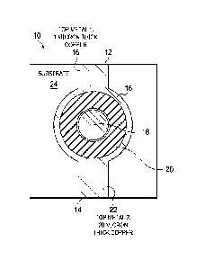
[0016] FIG. 1 shows an example of the device 10, that includes ports 12 and 14
that connect to
a top metal 16, which can be a copper layer that connected to, or shunted, to
a through-via hole
18. The design of the present invention reduces the variability from the
capacitor build. In this
design, the through-via hole is formed but does not affect the capacitor, thus
eliminating that
variable from design consideration(s). A top insulator 20 is positioned
between the top metal
16 at the via 18, and a second metal layer 22 is deposited on the insulator
20. The structure is
formed in a substrate 24.
[0017] FIG. 2 shows an internal view of the device 10, that shows the gap 26,
between the
through-hole via 18 and the first metal layer 16. Ports 12 and 14 that connect
to atop metal 16,
which can be a copper layer that connected to, or shunted, to a through-via
hole 18.
[0018] FIG. 3 is a cross-section side view of the device 10. Ports 12 and 14
are shown in this
configuration as being on opposite sides of the through-hole via 18, which is
isolated from the
top metal layer 16 and the second top metal layer 22, by insulator 20. A
bottom metal ground
plane 28 is depicted connected to through-hole via 18.
Date Recue/Date Received 2021-01-26
CA 03107812 2021-01-26
[0019] Table 1 and FIGS. 4A to 4F show a step-by-step method of making the
device 10 of the
present invention. The process flow to create a planarized surface in a
substrate with dissimilar
materials to eliminate vertical transitions from a substrate to an added
material is as follows:
Step 1. Lap and polish a substrate with the metal structures.
Step 2. Machine or etch a via or trench in the substrate, as shown in FIG. 4A
as a cross-sectional
side view that includes the substrate 24 into which the trench or via 18 is
cut or etched.
Step 3. Fill the via, ground plane or trench with copper using any of a number
of processes
including chemical vapor deposition (CVD), silkscreen, atomic layer deposition
(ALD) or other,
as shown in cross-sectional side view in FIG. 4B that shows the substrate 24
into which the trench
or via 18 is cut or etched, and the metal filled through-hole via 18 and a
ground plane 28. One
example is to selectively deposit tantalum on the sidewalls of the via or
trench structures and then
deposit copper organometallic by a silkscreen deposit. The filled substrate is
then heated in argon
to drive off /decompose the organic material and densify the copper. For the
copper deposited,
the adhesion layer is a few hundred angstroms of tantalum. The adhesion layer
may be removed
over the metal. The thickness of the metal/non substrate material needs to be
between two times
and ten times the transition step. The thickness of the deposited material can
be measured in real
time using a variety of techniques including, e.g., a crystal oscillator
during a vacuum deposition
processes, where one side of the via is connected to a ground plane.
Step 4. Coat the front side of the substrate with a photoresist and expose and
develop an annular
shape that circumscribes the via.
Step 5. Using a DC sputtering system, coat the photoresist with a copper
adhesion layer of a few
hundred angstroms of tantalum. Coat the substrate with 2 p.m of copper to form
the bottom
electrode, as shown in FIG. 4C, which is a top-view of the device 10. The
substrate 24 is shown
with throughOhole via 18, on which a bottom metal annular patter 30 is shown.
Step 6. Remove the photoresist to form a bottom electrode connected to the
via.
Step 7. Coat the front side of the substrate with a photoresist and expose and
develop an annular
shape that circumscribes the via, where the inner radii is between 2 p.m and
300 p.m from the outer
edge of the metal filled via and external radii of the pattern is between 10
p.m and 500 p.m
respectively.
Step 8. Using ALD or other deposition, deposit between 0.1 p.m and 101.im of a
dielectric material,
where the dielectric material has a dielectric constant between 2 and 2,000,
as shown in FIG. 4D,
Date Recue/Date Received 2021-01-26
CA 03107812 2021-01-26
6
which is a top view of the device 10. The substrate 24 is shown in which a gap
32 is depicted
between the through-hole via 18 and the second metal layer 22. Also depicted
is the insulator 20
(also referred to as a dielectric material).
Step 9. Remove the photoresist to form a dielectric region that is at least 1
p.m larger than the
bottom electrode.
Step 10. Coat the front side of the substrate with a photoresist and expose
and develop an annular
shape that is at least 2 i.tm greater than the dielectric layer and where one
side transitions to other
active or passive devices in the circuit.
Step 11. Using a DC sputtering system, coat the photoresist with a copper
adhesion layer is a few
hundred angstroms of tantalum. Coat the substrate with 2 p.m of copper to form
the top electrode.
Step 12. Remove the photoresist to form a top electrode for the capacitor
structure, which is
depicted in FIG. 4E, which shows the device 10, that now includes top metal
layer 22, disposed
on the insulator 20, and includes the gap 26, the bottom metal layer 16, the
through-hole via 18,
and the first metal layer 16.
Step 13. Coat the front side of the substrate with a photoresist and expose
and develop a
connecting metal line to both sides of the bottom metal of the annular
structure.
Step 14. Using a DC sputtering system, coat the photoresist with a copper
adhesion layer is a few
hundred angstroms of tantalum. Coat the substrate with 2 p.m of copper to form
the top electrode.
FIG. 4F shows the device 10, which now includes all the layers and ports 12
and 14.
[0020] It will be understood that particular embodiments described herein are
shown by way of
illustration and not as limitations of the invention. The principal features
of this invention can
be employed in various embodiments without departing from the scope of the
invention. Those
skilled in the art will recognize, or be able to ascertain using no more than
routine
experimentation, numerous equivalents to the specific procedures described
herein. Such
equivalents are considered to be within the scope of this invention and are
covered by the claims.
[0021] All publications and patent applications mentioned in the specification
are indicative of
the level of skill of those skilled in the art to which this invention
pertains.
[0022] The use of the word "a" or "an" when used in conjunction with the term
"comprising"
.. in the claims and/or the specification may mean "one," but it is also
consistent with the meaning
of "one or more," "at least one," and "one or more than one." The use of the
term "or" in the
claims is used to mean "and/or" unless explicitly indicated to refer to
alternatives only or the
Date Recue/Date Received 2021-01-26
CA 03107812 2021-01-26
7
alternatives are mutually exclusive, although the disclosure supports a
definition that refers to
only alternatives and "and/or." Throughout this application, the term "about"
is used to indicate
that a value includes the inherent variation of error for the device, the
method being employed
to determine the value, or the variation that exists among the study subjects.
.. [0023] As used in this specification and claim(s), the words "comprising"
(and any form of
comprising, such as "comprise" and "comprises"), "having" (and any form of
having, such as
"have" and "has"), "including" (and any form of including, such as "includes"
and "include")
or "containing" (and any form of containing, such as "contains" and "contain")
are inclusive or
open-ended and do not exclude additional, unrecited elements or method steps.
In embodiments
of any of the compositions and methods provided herein, "comprising" may be
replaced with
"consisting essentially of' or "consisting of'. As used herein, the phrase
"consisting essentially
of' requires the specified integer(s) or steps as well as those that do not
materially affect the
character or function of the claimed invention. As used herein, the term
"consisting" is used to
indicate the presence of the recited integer (e.g., a feature, an element, a
characteristic, a
property, a method/process step or a limitation) or group of integers (e.g.,
feature(s), element(s),
characteristic(s), property(ies), method/process steps or limitation(s)) only.
[0024] The term "or combinations thereof' as used herein refers to all
permutations and
combinations of the listed items preceding the term. For example, "A, B, C, or
combinations
thereof' is intended to include at least one of: A, B, C, AB, AC, BC, or ABC,
and if order is
important in a particular context, also BA, CA, CB, CBA, BCA, ACB, BAC, or
CAB.
Continuing with this example, expressly included are combinations that contain
repeats of one
or more item or term, such as BB, AAA, AB, BBC, AAABCCCC, CBBAAA, CABABB, and
so forth. The skilled artisan will understand that typically there is no limit
on the number of
items or terms in any combination, unless otherwise apparent from the context.
[0025] As used herein, words of approximation such as, without limitation,
"about",
"substantial" or "substantially" refers to a condition that when so modified
is understood to not
necessarily be absolute or perfect but would be considered close enough to
those of ordinary
skill in the art to warrant designating the condition as being present. The
extent to which the
description may vary will depend on how great a change can be instituted and
still have one of
ordinary skilled in the art recognize the modified feature as still having the
required
characteristics and capabilities of the unmodified feature. In general, but
subject to the preceding
discussion, a numerical value herein that is modified by a word of
approximation such as
"about" may vary from the stated value by at least +1, 2, 3, 4, 5, 6, 7, 10,
12 or 15%.
Date Recue/Date Received 2021-01-26
CA 03107812 2021-01-26
8
[0026] All of the compositions and/or methods disclosed and claimed herein can
be made and
executed without undue experimentation in light of the present disclosure.
While the
compositions and methods of this invention have been described in terms of
preferred
embodiments, it will be apparent to those of skill in the art that variations
may be applied to the
compositions and/or methods and in the steps or in the sequence of steps of
the method described
herein without departing from the scope of the invention. All such similar
substitutes and
modifications apparent to those skilled in the art are deemed to be within the
scope of the
invention as defined by the appended claims.
Date Recue/Date Received 2021-01-26