Note : Les descriptions sont présentées dans la langue officielle dans laquelle elles ont été soumises.
CA 03109344 2021-02-10
1
DESCRIPTION
RADIATION MEASUREMENT DEVICE
TECHNICAL FIELD
[0001] The present disclosure relates to a radiation
measurement device for measuring a detection pulse obtained
by a radiation detector.
BACKGROUND ART
[0002] In general, in a radiation measurement device,
after a detection pulse obtained by a radiation detector is
amplified by an amplifier, only detection pulses within a
range between lower and upper thresholds (Lsh, Hsh, where Lsh
< Hsh) set in advance are extracted by a pulse height
selection circuit in order to remove noise components and the
like, and the extracted detection pulses are counted to
measure the intensity of radiation.
[0003] A conventional pulse height selection circuit is
formed by a one-shot multivibrator having elements such as a
resistor R and a capacitor C, and a delay circuit using a
response time of a logic IC having elements such as a
capacitor C and a reactor L, thus achieving a function of
extracting detection pulses within a range between the lower
and upper thresholds (Lsh, Hsh) (see, for example, Patent
Document 1).
Date Recue/Date Received 2021-02-10
CA 03109344 2021-02-10
2
CITATION LIST
PATENT DOCUMENT
[0004] Patent Document 1: Japanese Laid-Open Patent
Publication No. 2014-1951
SUMMARY OF THE INVENTION
PROBLEMS TO BE SOLVED BY THE INVENTION
[0005] As described above, the pulse height selection
circuit in the conventional radiation measurement device is
formed by a one-shot multivibrator having elements such as a
resistor R and a capacitor C, and a delay circuit using a
response time of a logic IC having elements such as a
capacitor C and a reactor L. Therefore, there is a problem
that, due to variation in characteristics of the elements
such as the resistor R and the capacitor C, the pulse width
of an output pulse from the one-shot multivibrator or the
delay time of the delay circuit is not stable. As a result,
for example, count loss of detection pulses occurs or
unnecessary detection pulses that should be excluded through
pulse height selection are also measured, thus causing a
fault such as occurrence of error in a measurement result.
[0006] The present disclosure has been made to solve the
above problem, and an object of the present disclosure is to
provide a radiation measurement device that can always stably
Date Recue/Date Received 2021-02-10
CA 03109344 2021-02-10
3
and assuredly extract only detection pulses within a range
between the lower and upper thresholds (Lsh, Hsh) from
detection pulses obtained by a radiation detector, thus
enabling more accurate measurement for the intensity of
radiation than conventional art.
SOLUTION TO THE PROBLEMS
[0007] A radiation measurement device according to the
present disclosure includes: a first pulse height detection
circuit for outputting a first pulse height detection signal
which rises when a detection pulse outputted from a radiation
detector becomes greater than a lower threshold Lsh, and
falls when the detection pulse becomes smaller than the lower
threshold Lsh; a second pulse height detection circuit for
outputting a second pulse height detection signal which rises
when the detection pulse outputted from the radiation
detector becomes greater than an upper threshold Hsh greater
than the lower threshold Lsh, and falls when the detection
pulse becomes smaller than the upper threshold Hsh; a crystal
oscillator for generating a clock pulse with a certain cycle;
a first rising and falling detection circuit for detecting
both rising and falling edges of the first pulse height
detection signal outputted from the first pulse height
detection circuit, in synchronization with the clock pulse
from the crystal oscillator; a second rising and falling
Date Recue/Date Received 2021-02-10
CA 03109344 2021-02-10
4
detection circuit for detecting both rising and falling edges
of the second pulse height detection signal outputted from
the second pulse height detection circuit, in synchronization
with the clock pulse from the crystal oscillator; and a
combining circuit for outputting a signal corresponding to
the detection pulse that is within a range between the lower
threshold Lsh and the upper threshold Hsh, by combining an
output from the first rising and falling detection circuit
and an output from the second rising and falling detection
circuit, in synchronization with the clock pulse from the
crystal oscillator.
EFFECT OF THE INVENTION
[0008] In the radiation measurement device according to
the present disclosure, with respect to detection pulses
obtained by the radiation detector, only a detection pulse
having a pulse height value within a range between the lower
threshold Lsh and the upper threshold Hsh can be always
stably and assuredly extracted in synchronization with the
clock pulse from the crystal oscillator, thus enabling
accurate measurement for the intensity of radiation.
BRIEF DESCRIPTION OF THE DRAWINGS
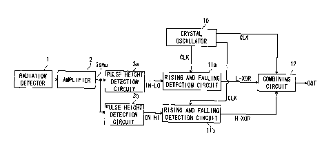
[0009] [FIG. 1] FIG. 1 is a block diagram showing the
schematic configuration of a radiation measurement device in
Date Recue/Date Received 2021-02-10
CA 03109344 2021-02-10
a reference example for the present disclosure.
[FIG. 2] FIG. 2 is a timing chart for illustrating
operation of the radiation measurement device in the
reference example for the present disclosure.
5 [FIG. 3] FIG. 3 shows a truth table of the
radiation measurement device in the reference example of the
present disclosure.
[FIG. 4] FIG. 4 is a block diagram showing the
schematic configuration of a radiation measurement device
according to embodiment 1.
[FIG. 5] FIG. 5 is a block diagram showing the
details of a rising and falling detection circuit and a
combining circuit of the radiation measurement device
according to embodiment 1.
[FIG. 6] FIG. 6 is a timing chart for illustrating
operation of the radiation measurement device according to
embodiment 1.
[FIG. 7] FIG. 7 shows a truth table of the
radiation measurement device according to embodiment 1.
[FIG. 8] FIG. 8 is a block diagram showing the
schematic configuration of a radiation measurement device
according to embodiment 2.
[FIG. 9] FIG. 9 is a block diagram showing the
details of a pulse width detection circuit of the radiation
measurement device according to embodiment 2.
Date Recue/Date Received 2021-02-10
CA 03109344 2021-02-10
6
DESCRIPTION OF EMBODIMENTS
[0010] For the purpose of further understanding of the
contents of the present disclosure, the configuration of
technology as a reference for the present disclosure and a
problem thereof will be described below in advance.
[0011] FIG. 1 is a block diagram showing the schematic
configuration of a radiation measurement device in a
reference example for the present disclosure, and FIG. 2 is a
timing chart for illustrating operation of the radiation
measurement device in the reference example for the present
disclosure.
[0012] The radiation measurement device as the reference
example in FIG. 1 includes a radiation detector 1, an
amplifier 2, a first pulse height detection circuit 3a, a
second pulse height detection circuit 3b, a first one-shot
circuit 4a, a second one-shot circuit 4b, an OR circuit 5, a
first delay circuit 6a, a second delay circuit 6b, a
combining circuit 7, and an AND circuit 8. It is noted that
the latter stage circuit excluding the radiation detector 1
and the amplifier 2 corresponds to a pulse height selection
circuit.
[0013] The radiation detector 1 is formed from, for
example, a scintillation counter, a semiconductor detector,
or the like, and outputs a detection pulse in accordance with
Date Recue/Date Received 2021-02-10
CA 03109344 2021-02-10
7
the intensity of radiation. The amplifier 2 outputs a
detection pulse lamp obtained by amplifying the detection
pulse detected by the radiation detector 1 to a predetermined
level, as shown in (a) of FIG. 2.
[0014] The first pulse height detection circuit 3a outputs
a first pulse height detection signal IN-LO which rises when
the signal level of the detection pulse lamp amplified by the
amplifier 2 becomes greater than a certain lower threshold
Lsh set in advance, and falls when the signal level becomes
smaller than the lower threshold Lsh, as shown in (b) of FIG.
2. The second pulse height detection circuit 3b outputs a
second pulse height detection signal IN-HI which rises when
the signal level of the detection pulse lamp amplified by the
amplifier 2 becomes greater than a certain upper threshold
Hsh (Hsh > Lsh) set in advance, and falls when the signal
level becomes smaller than the upper threshold Hsh, as shown
in (c) of FIG. 2.
[0015] The first one-shot circuit 4a is formed from a
monostable one-shot multivibrator having elements such as a
resistor R and a capacitor C, and outputs a pulse signal LO
having a predetermined pulse width Ti in accordance with
rising of the first pulse height detection signal IN-LO from
the first pulse height detection circuit 3a, as shown in (d)
of FIG. 2. Similarly, the second one-shot circuit 4b is
formed from a monostable one-shot multivibrator having
Date Recue/Date Received 2021-02-10
CA 03109344 2021-02-10
8
elements such as a resistor R and a capacitor C, and outputs
a pulse signal HI having a predetermined pulse width Ti in
accordance with rising of the second pulse height detection
signal IN-HI, as shown in (e) of FIG. 2.
[0016] The OR circuit 5 combines the output LO of the
first one-shot circuit 4a and the output HI of the second
one-shot circuit 4b, and outputs both as a clock pulse CLK.
[0017] The first delay circuit 6a is formed from a logic
IC having elements such as a capacitor C and a reactor L, and
outputs a pulse signal LO-D delayed by a certain time T2 from
the pulse signal LO outputted from the first one-shot circuit
4a, as shown in (f) of FIG. 2. Similarly, the second delay
circuit 6b is formed from a logic IC having elements such as
a capacitor C and a reactor L, and outputs a pulse signal HI-
D delayed by the certain time T2 from the pulse signal HI
outputted from the second one-shot circuit 4b, as shown in
(g) of FIG. 2.
[0018] The combining circuit 7 is formed from, in this
example, a JK flip-flop, and is configured such that the
pulse signal LO-D outputted from the first delay circuit 6a
is inputted to a J input terminal, the pulse signal HID
outputted from the second delay circuit 6b is inputted to a K
input terminal, and the pulse signal LO outputted from the
first one-shot circuit 4a and the pulse signal HI outputted
from the second one-shot circuit 4b are both inputted through
Date Recue/Date Received 2021-02-10
CA 03109344 2021-02-10
9
the OR circuit 5 as the clock pulse CLK to a sampling
terminal T. As a result, a rectangular-wave signal OUT1 as
shown in (h) of FIG. 2 is outputted from an output terminal Q
of the combining circuit 7 in accordance with a truth table
shown in FIG. 3.
[0019] The AND circuit 8 makes a logical conjunction of
the output signal OUT1 from the combining circuit 7 and the
pulse signal LO-D outputted from the first delay circuit 6a,
and a pulse signal OUT2 as shown in (i) of FIG. 2 is
outputted from the AND circuit 8.
[0020] Here, when the pulse height value of the pulse
signal lamp outputted from the amplifier 2 becomes greater
than the upper threshold Hsh, the output OUT2 of the AND
circuit 8 has a pulse width T3 shorter than the pulse width
Ti of the output LO of the first one-shot circuit 4a, and
meanwhile, when the pulse height value of the pulse signal
lamp outputted from the amplifier 2 is within a range between
the upper threshold Hsh and the lower threshold Lsh, the
output OUT2 of the AND circuit has the same pulse width Ti as
the pulse signal LO of the first one-shot circuit 4a.
[0021] With respect to the output pulse OUT2 from the AND
circuit 8, thereafter, a signal having a pulse width smaller
than the pulse width Ti is excluded by a pulse width
selection circuit (not shown). Therefore, finally, only
pulses in the case where the pulse height value of the pulse
Date Recue/Date Received 2021-02-10
CA 03109344 2021-02-10
signal lamp outputted from the amplifier 2 is within a range
between the upper threshold Hsh and the lower threshold Lsh,
are extracted.
[0022] However, as described above, the first one-shot
5 circuit 4a and the second one-shot circuit 4b have elements
such as the resistor R and the capacitor C, and the first
delay circuit 6a and the second delay circuit 6b are
configured using a response time of the logic IC having
elements such as the capacitor C and the reactor L.
10 Therefore, due to variation in characteristics of these
elements, the pulse widths of the output pulses LO, HI of the
first one-shot circuit 4a and the second one-shot circuit 4b,
or the delay times T2 of the first delay circuit 6a and the
second delay circuit 6b, are not stable. As a result, for
example, count loss of detection pulses occurs or unnecessary
detection pulses that should be excluded through pulse height
selection are also measured, thus causing a fault such as
occurrence of error in a measurement result. The present
disclosure is to provide a radiation measurement device that
prevents such a fault. Hereinafter, embodiments of the
present disclosure will be described.
[0023] Embodiment 1
FIG. 4 is a block diagram showing the schematic
configuration of a radiation measurement device according to
embodiment 1, and FIG. 5 is a block diagram showing the
Date Recue/Date Received 2021-02-10
CA 03109344 2021-02-10
11
details of a rising and falling detection circuit and a
combining circuit of the radiation measurement device
according to embodiment 1. FIG. 6 is a timing chart for
illustrating operation of the radiation measurement device
according to embodiment 1.
[0024] The radiation measurement device of embodiment 1
includes a radiation detector 1, an amplifier 2, a first
pulse height detection circuit 3a, a second pulse height
detection circuit 3b, a crystal oscillator 10, a first rising
and falling detection circuit 11a, a second rising and
falling detection circuit 11b, and a combining circuit 12.
[0025] The radiation detector 1 is formed from, for
example, a scintillation counter, a semiconductor detector,
or the like, and outputs a detection pulse in accordance with
the intensity of radiation. The amplifier 2 outputs a
detection pulse lamp obtained by amplifying the detection
pulse from the radiation detector 1 to a predetermined level,
as shown in (a) of FIG. 6.
[0026] The first pulse height detection circuit 3a outputs
a first pulse height detection signal IN-LO which rises when
the signal level of the amplified detection pulse lamp
becomes greater than a certain lower threshold Lsh set in
advance, and falls when the signal level becomes smaller than
the certain lower threshold Lsh, as shown in (b) of FIG. 6.
The second pulse height detection circuit 3b outputs a second
Date Recue/Date Received 2021-02-10
CA 03109344 2021-02-10
12
pulse height detection signal IN-HI which rises when the
signal level of the detection pulse lamp amplified becomes
greater than a certain upper threshold Hsh (Hsh > Lsh) set in
advance, and falls when the signal level becomes smaller than
the certain upper threshold Hsh, as shown in (c) of FIG. 6.
[0027] The crystal oscillator 10 outputs a clock pulse CLK
having a stable constant frequency as shown in (d) of FIG. 6.
[0028] The first rising and falling detection circuit 11a
is, as shown in FIG. 5, formed from a D flip-flop 15 and an
XOR circuit (exclusive disjunction circuit) 16, and as shown
in (e) of FIG. 6, detects rising and falling edges of the
first pulse height detection signal IN-LO from the first
pulse height detection circuit 3a in synchronization with the
clock pulse CLK from the crystal oscillator 10, and according
to each detection, outputs a pulse signal L-XOR having a
certain pulse width Ta.
The second rising and falling detection circuit 11b
is, as shown in FIG. 5, formed from a D flip-flop 17 and an
XOR circuit (exclusive disjunction circuit) 18, and as shown
in (f) of FIG. 6, detects a rising edge and a falling edge of
the second pulse height detection signal IN-HI from the
second pulse height detection circuit 3b in synchronization
with the clock pulse CLK from the crystal oscillator 10, and
according to each detection, outputs a pulse signal H-XOR
having the certain pulse width Ta.
Date Recue/Date Received 2021-02-10
CA 03109344 2021-02-10
13
[0029] The combining circuit 12 receives the pulse signal
L-XOR outputted from the first rising and falling detection
circuit 11a and the pulse signal H-XOR outputted from the
second rising and falling detection circuit 11b, and finally,
only when the pulse height value of the pulse signal lamp
outputted from the amplifier 2 is within a range between the
upper threshold Hsh and the lower threshold Lsh described
above, the combining circuit 12 outputs a signal OUT
corresponding thereto as shown in (j) of FIG. 6, in
synchronization with the clock pulse CLK from the crystal
oscillator 10.
[0030] FIG. 5 shows specific details of the combining
circuit 12 for realizing the above function.
The combining circuit 12 in embodiment 1 includes a
first AND circuit 19, an XOR circuit 20, a second AND circuit
21, a first JK flip-flop 22, a third AND circuit 23, a fourth
AND circuit 24, a NOR circuit (joint denial circuit) 25, and
a second JK flip-flop 26.
[0031] Output of the first AND circuit 19 is "H" when the
pulse signal L-XOR outputted from the first rising and
falling detection circuit 11a and a later-described pulse
signal Trig outputted from the second JK flip-flop 26 are
both inputted (i.e., when both are "H").
[0032] When the pulse signal L XOR and the pulse signal
Trig are both inputted to the first AND circuit 19 (i.e.,
Date Recue/Date Received 2021-02-10
CA 03109344 2021-02-10
14
both are "H") and the pulse signal H-XOR is not outputted
from the second rising and falling detection circuit 11b
(i.e., the output lamp of the amplifier 2 is not greater than
the upper threshold Hsh), output of the XOR circuit 20 is "H"
and therefore output of the second AND circuit 21 is also
"H". On the other hand, even when the pulse signal L XOR and
the pulse signal Trig are both inputted to the first AND
circuit 19, if the pulse signal H-XOR is outputted from the
second rising and falling detection circuit 11b (i.e., the
output lamp of the amplifier 2 is greater than the upper
threshold Hsh), output of the XOR circuit 20 is "L" and
therefore output of the second AND circuit 21 is also "L".
[0033] In the first JK flip-flop 22, output of the second
AND circuit 21 is inputted to both of a J input terminal and
a K input terminal, and the clock pulse CLK from the crystal
oscillator 10 is inputted to a sampling terminal T.
Therefore, in a state in which output of the second AND
circuit 21 is "H", every time the clock pulse CLK is inputted
(specifically, at the timing of falling of the clock pulse
CLK), the first JK flip-flop 22 accordingly outputs the pulse
signal OUT with its level inverted at each time as shown in
(j) of FIG. 6, from an output terminal Q thereof.
[0034] As shown in (g) of FIG. 6, the third AND circuit 23
extracts, from the pulse signal L-XOR outputted from the
first rising and falling detection circuit 11a, a pulse
Date Recue/Date Received 2021-02-10
CA 03109344 2021-02-10
signal generated along with rising of the first pulse height
detection signal IN-LO from the first pulse height detection
circuit 3a, thus outputting an extracted pulse Sa.
[0035] The fourth AND circuit 24 and the NOR circuit
5 (joint denial circuit) 25 extract, from the pulse signal L-
XOR outputted from the first rising and falling detection
circuit 11a, a pulse signal outputted along with falling of
the first pulse height detection signal IN-LO from the first
pulse height detection circuit 3a, and extract the pulse
10 signal H-XOR outputted from the second rising and falling
detection circuit 11b, thus outputting an extracted pulse Sb
as shown in (h) of FIG. 6.
[0036] In the second JK flip-flop 26, the extracted pulse
Sa outputted from the third AND circuit 23 is inputted to a J
15 input terminal, the extracted pulse Sb outputted from the NOR
circuit 25 is inputted to a K input terminal, and the clock
pulse CLK from the crystal oscillator 10 is inputted to a
sampling terminal T. Therefore, in accordance with a truth
table as shown in FIG. 7, every time the clock pulse CLK is
inputted (specifically, at the timing of falling of the clock
pulse CLK), the second JK flip-flop 26 accordingly outputs a
pulse signal Trig as shown in (i) of FIG. 6 from an output
terminal Q.
[0037] For example, in FIG. 7, in the case where the
extracted pulse Sa outputted from the third AND circuit 23 is
Date Recue/Date Received 2021-02-10
CA 03109344 2021-02-10
16
"H" and the extracted pulse Sb outputted from the NOR circuit
25 is "L", the pulse signal Trig rises at the timing of
falling of the clock pulse CLK, and in the case where the
extracted pulse Sa outputted from the third AND circuit 23 is
"L" and the extracted pulse Sb outputted from the NOR circuit
25 is "H", the pulse signal Trig falls at the timing of
falling of the clock pulse CLK.
[0038] Thus, from the output terminal Q of the first JK
flip-flop 22, as shown in (j) of FIG. 6, only in the case
where the pulse height value of the detection pulse lamp
outputted from the amplifier 2 is between the upper threshold
Hsh and the lower threshold Lsh described above, the signal
OUT is outputted in synchronization with the clock pulse CLK
from the crystal oscillator 10 while the level of the signal
OUT is inverted accordingly, and in the case where the pulse
height value is out of the range between the upper threshold
Hsh and the lower threshold Lsh, the output OUT from the
output terminal Q of the first JK flip-flop 22 is inhibited.
[0039] As described above, in the radiation measurement
device according to the present embodiment 1, with respect to
the detection pulses obtained by the radiation detector 1,
only when the pulse height value thereof is within a range
between the upper threshold Lsh and the lower threshold Hsh,
the pulse can be extracted in synchronization with the clock
pulse from the crystal oscillator 10. Thus, it becomes
Date Recue/Date Received 2021-02-10
CA 03109344 2021-02-10
17
possible to measure the intensity of radiation always stably
and assuredly, so that detection accuracy in radiation
measurement is enhanced.
[0040] Embodiment 2
FIG. 8 is a block diagram showing the schematic
configuration of a radiation measurement device according to
embodiment 2. The components that correspond to or are the
same as those of the radiation measurement device in
embodiment 1 shown in FIG. 4 are denoted by the same
reference characters. FIG. 9 is a block diagram showing the
details of a pulse width detection circuit of the radiation
measurement device according to embodiment 2.
[0041] The pulse width of the detection pulse obtained by
the radiation detector 1 is determined depending on a
physical phenomenon, and thus, if a pulse width W of the
detection pulse lamp amplified by the amplifier 2 is greater
than a predetermined threshold Wsh, the pulse is considered
to be noise. As a factor for causing such noise, it is
assumed that, for example, noise is superimposed on cables
connecting the radiation detector 1 and various signal
processing circuits at a stage subsequent thereto.
[0042] Accordingly, in embodiment 2, a pulse width
detection circuit 13 is provided which compares the pulse
width W of the first pulse height detection signal IN-LO
outputted from the first pulse height detection circuit with
Date Recue/Date Received 2021-02-10
CA 03109344 2021-02-10
18
a certain threshold Wsh set in advance as a permissible pulse
width, and inhibits the pulse output OUT of the combining
circuit 12 when the pulse width W of the first pulse height
detection signal IN-LO is greater than the threshold Wsh (W >
Wsh).
[0043] As a specific example, the pulse width detection
circuit 13 includes a counter circuit 31, a pulse width
setting device 32, and a comparator circuit 33 as shown in
FIG. 9.
During a period in which the first pulse height
detection signal IN-LO outputted from the first pulse height
detection circuit 3a is "H", the counter circuit 31 counts
the clock pulses CLK from the crystal oscillator 10 (this
count corresponds to the pulse width W of the first pulse
height detection signal IN-LO), and the comparator circuit 33
compares a count value C of the above count with a count
value Csh set in advance in the pulse width setting device 32
(this count value Csh corresponds to the certain threshold
Wsh set as a permissible value).
[0044] Then, when the count value C of the counter circuit
31 is smaller than the count value Csh set in advance in the
pulse width setting device 32 (i.e., W Wsh), a signal of
"H" is generated, and when the count value C is greater than
the count value Csh (i.e., W > Wsh), a signal of "L" is
generated. These signals are outputted to the combining
Date Recue/Date Received 2021-02-10
CA 03109344 2021-02-10
19
circuit 12 (specifically, second AND circuit 21).
[0045] Thus, when output of the pulse width detection
circuit 13 is "H", i.e., when the pulse width W of the
detection pulse lamp obtained through the amplifier 2 from
the radiation detector 1 is smaller than the predetermined
threshold Wsh (W Wsh), the pulse output OUT of the
combining circuit 12 is permitted, but when output of the
pulse width detection circuit 13 is "L", i.e., when the pulse
width W of the detection pulse lamp obtained through the
amplifier 2 from the radiation detector 1 is greater than the
predetermined threshold Wsh (W > Wsh), the pulse is
considered to be noise, so that the pulse output OUT of the
combining circuit 12 is inhibited.
The other configurations, operations, and effects
are the same as those in embodiment 1, and therefore the
detailed description thereof is omitted here.
[0046] As described above, in embodiment 2, unnecessary
noise components contained in the detection pulse lamp can be
assuredly prevented from being extracted together, whereby it
becomes possible to measure the intensity of radiation more
accurately than in embodiment 1.
[0047] Although the disclosure is described above in terms
of various exemplary embodiments and implementations, it
should be understood that the various features, aspects, and
functionality described in one or more of the individual
Date Recue/Date Received 2021-02-10
CA 03109344 2021-02-10
embodiments are not limited in their applicability to the
particular embodiment with which they are described, but
instead can be applied, alone or in various combinations to
one or more of the embodiments of the disclosure.
5 [0048] It is therefore understood that numerous
modifications which have not been exemplified can be devised
without departing from the scope of the present disclosure.
For example, at least one of the constituent components may
be modified, added, or eliminated. At least one of the
10 constituent components mentioned in at least one of the
preferred embodiments may be selected and combined with the
constituent components mentioned in another preferred
embodiment.
15 DESCRIPTION OF THE REFERENCE CHARACTERS
[0049] 1 radiation detector
2 amplifier
3a first pulse height detection circuit
3b second pulse height detection circuit
20 10 crystal oscillator
11a first rising and falling detection circuit
lib second rising and falling detection circuit
12 combining circuit
13 pulse width detection circuit
Lsh lower threshold
Date Recue/Date Received 2021-02-10
CA 03109344 2021-02-10
21
Hsh upper threshold
Date Recue/Date Received 2021-02-10