Note : Les descriptions sont présentées dans la langue officielle dans laquelle elles ont été soumises.
CA 03110219 2021-02-19
WO 2020/047508 PCT/US2019/049221
ULTRAFAST PARTICLE SORTING
CROSS-REFERENCE
[0001] This application claims the benefit of U.S. Provisional Patent
Application No.
62/725358, filed August 31, 2018, which application is incorporated herein by
reference.
BACKGROUND OF THE INVENTION
[0002] Cell-based therapies represent a cornerstone of regenerative medicine
and
immunotherapies. While many of the non-therapeutic cells that carry over into
the therapy are
harmless, even a small population of a specific errant cell type can cause
severely adverse
consequences in the patient. Therefore, it can be critical to purify the
therapeutic cells away from
the deleterious cells before transplanting the cells into a patient. To
accelerate the translation of
cell-based regenerative medicine techniques into the clinic, high-throughput,
high-purity
methods to isolate rare stem cells and other immune cell types based on
differential surface
marker expression in a sterile and clinically applicable format can be
necessary.
SUMMARY OF THE INVENTION
[0003] Embodiments disclosed herein provide systems, methods, and devices for
sorting cells.
In some instances, the cells can be sorted with aid of lasers (e.g., laser
extraction) and/or
micropore arrays. The micropore arrays can comprise a coating that can
interact with the lasers
to aid in extraction of cells of interest. The coating can in some instances
peel off and
concurrently disrupt a meniscus of a liquid held in the micropore array.
Advantageously, the
approaches described herein can increase cell viability and extraction
efficiency, for example, as
lasers are directed to surfaces of the array rather than directly at the
liquid holding the particles
of interest.
[0004] In some aspects, the disclosure provides an array, the array comprising
a substrate with
a first surface and a second surface opposite the first surface, wherein the
substrate comprises a
substrate material and a surface material wherein the surface material is
positioned at or adjacent
to the first or second surfaces, and the substrate comprises a plurality of
pores defining lumens
extending from the first surface to the second surface and wherein the
substrate is characterized
by: each pore of the plurality of pores has a largest diameter of 500 microns
or less, each pore of
the plurality of pores has an aspect ratio of 10 or greater, and the surface
material is selected
from a material that absorbs greater than 10 percent of incident
electromagnetic radiation.
[0005] In some aspects, the disclosure provides an array comprising: a
substrate with a first
surface and a second surface opposite the first surface, wherein the substrate
comprises a
substrate material and a surface material wherein the surface material is
positioned at or adjacent
-1-
CA 03110219 2021-02-19
WO 2020/047508 PCT/US2019/049221
to the first or second surfaces, and the substrate comprises a plurality of
pores extending from the
first surface to the second surface and wherein the substrate is characterized
by: a pore density of
100 or greater pores per square millimeter, each pore of the plurality of
pores has an aspect ratio
of 10 greater, and the surface material is selected from a material that
absorbs greater than 10
percent of incident electromagnetic radiation.
[0006] In certain embodiments, each pore has a largest cross-sectional area of
about 0.008 mm2
or less. In certain embodiments, each pore of the plurality of pores has a
pore diameter within a
range from 5 microns to 100 microns. In certain embodiments, each pore of the
plurality of
pores has a pore diameter within a range from 15 microns to 50 microns. In
certain
embodiments, each pore has a length selected range from about 1 mm to about
500 mm. In
certain embodiments, each pore has a length selected from a range from about
lmm to about 100
mm. In certain embodiments, each pore has a length selected from a range from
about 1 mm to
about 10 mm.
[0007] In certain embodiments, the pore density is within a range from 100 to
2500 pores per
square millimeter. In certain embodiments, the pore density is within a range
from 500 to 1500
pores per square millimeter. In certain embodiments, the surface material is
substantially similar
to the substrate material. In certain embodiments, the surface material is
different than the
substrate material. In certain embodiments, the substrate material is glass
and the surface
material is not glass. In certain embodiments, the surface material comprises
a metal. In certain
embodiments, the surface material absorbs greater than 10 percent of incident
electromagnetic
radiation of a wavelength selected from 0.4 microns to 2.5 microns. In certain
embodiments, the
surface material absorbs greater than 50 percent of incident radiation. In
certain embodiments,
the surface material absorbs greater than 50 percent of incident
electromagnetic radiation of a
wavelength selected from 0.4 microns to 1.5 microns.
[0008] In certain embodiments, the aspect ratio is within a range from 10 to
100. In certain
embodiments, the aspect ratio is 20 or greater. In certain embodiments, the
aspect ratio is 50 or
greater. In certain embodiments, the aspect ratio is 100 or greater. In
certain embodiments, the
surface material coats or partially coats the second surface. In certain
embodiments, the surface
material coats or partially coats the first surface. In certain embodiments,
the surface material
does not block access to the lumens of the pores. In certain embodiments, the
surface material
has an average thickness of about 20 nm to 500 nm. In certain embodiments, the
surface
material has an average thickness of about 100 nm to 500 nm. In certain
embodiments, the
surface material is hydrophobic.
[0009] In certain embodiments, the first and second surfaces are substantially
parallel planes.
In certain embodiments, the plurality of pores extends at an angle relative to
a surface normal
-2-
CA 03110219 2021-02-19
WO 2020/047508 PCT/US2019/049221
from the first surface to the second surface. In certain embodiments, the
angle is greater within a
range from zero to ninety degrees. In certain embodiments, the plurality of
pores extends
orthogonally from the first surface to the second surface. In certain
embodiments, the plurality of
pores traverses an indirect path from the first surface to the second surface.
[0010] In some aspects, the present disclosure provides a system for sorting
components of a
mixture, comprising the array of any aspect of the present disclosure and a
housing comprising
an internal surface configured to receive selected contents released from the
array. In certain
embodiments, the internal surface is positioned below the second surface of
the substrate.
[0011] In some aspects, the present disclosure provides a method of releasing
selected contents
from a pore of an array, the method comprising: identifying a pore of an array
with selected
contents, wherein the array comprises a substrate with a first surface and a
second surface
opposite the first surface, wherein the substrate comprises a substrate
material and a surface
material wherein the surface material is positioned at or adjacent to the
first or second surfaces,
and the substrate comprises a plurality of pores defining lumens extending
from the first surface
to the second surface, wherein the substrate is characterized by one or more
of: (a) each pore of
the plurality of pores has a largest diameter of 500 microns or less, (b) each
pore of the plurality
of pores has an aspect ratio of 10 or greater, (c) a pore density of 100 or
greater pores per square
millimeter, and (d) the surface material is selected from a material that
absorbs greater than 10
percent of incident electromagnetic radiation, and removing a portion of the
surface material
from the first or second surface of the array with electromagnetic radiation
directed to the surface
material within or adjacent to the identified pore, thereby releasing the
contents of the identified
pore.
[0012] In certain embodiments, the electromagnetic radiation is selected from
a wavelength of
0.2 microns to 2.5 microns, a fluence level sufficient to disrupt adhesion
between the contents
and the pore, and a pulse duration in a range from 1 ns to 1 millisecond. In
certain embodiments,
removing surface material comprises ablation. In certain embodiments, removing
surface
material comprises mechanical removal. In certain embodiments, mechanical
removal comprises
chipping. In certain embodiments, removing surface material comprises
photothermal removal.
In certain embodiments, removing surface material comprises photochemical
removal. In certain
embodiments, removing surface material comprises photoacoustic removal.
[0013] In certain embodiments, the selected contents comprise cells in an
aqueous solution. In
certain embodiments, the cells are selected from INKT cells, Tmem, Treg,
HSPCs, and
combinations thereof In certain embodiments, each pore of the plurality of
pores has a cross-
sectional area each of about 0.008 mm2 or less. In certain embodiments, each
pore of the
plurality of pores has a pore diameter within a range from 5 microns to 100
microns. In certain
-3-
CA 03110219 2021-02-19
WO 2020/047508 PCT/US2019/049221
embodiments, each pore of the plurality of pores has a pore diameter within a
range from 15
microns to 50 microns. In certain embodiments, each pore has a length selected
range from
about 1 mm to about 500 mm. In certain embodiments, each pore has a length
selected from a
range from about lmm to about 100 mm. In certain embodiments, each pore has a
length
selected from a range from about 1 mm to about 10 mm.
[0014] In certain embodiments, the pore density is within a range from 100 to
2500 pores per
square millimeter on an array. In certain embodiments, the pore density is
within a range from
500 to 1500 pores per square millimeter of an array. In certain embodiments,
the array comprises
a pore density of greater than 1000 pores/mm2. In certain embodiments, pore
density is 5000
pores/mm2 or greater. In certain embodiments, the aspect ratio is within a
range from 10 to 100.
In certain embodiments, the pores have an aspect ratio of 20 or greater. In
certain embodiments,
the pores have an aspect ratio of 50 or greater. In certain embodiments, the
pores have an aspect
ratio of 100 or greater. In certain embodiments, the surface material absorbs
greater than 10
percent at a wavelength selected from about 0.4 micron to about 2.5 micron. In
certain
embodiments, the surface material absorbs of greater than 50 percent of
incident radiation. In
certain embodiments, the surface material absorbs greater than 50 percent of
incident radiation at
a wavelength selected from about 0.4 micron to about 2.5 micron.
[0015] In certain embodiments, the array is characterized by two or more of:
(a) each pore of
the plurality of pores has a largest diameter of 500 microns or less, (b) each
pore of the plurality
of pores has an aspect ratio of 10 or greater, (c) a pore density of 100 or
greater pores per square
millimeter, and (d) the surface material is selected from a material that
absorbs greater than 10
percent of incident electromagnetic radiation. In certain embodiments, the
portion of the surface
material is adjacent to the identified pore. In certain embodiments, the
portion of the surface
comprises a luminal surface of the identified pore. In certain embodiments,
the portion of the
surface is removed to a depth of 100 microns or less. In certain embodiments,
the portion of the
surface is removed to a depth of 50 microns or less. In certain embodiments,
the method further
comprises loading the array with a solution comprising the selected contents
prior to the
identifying the pore with selected contents. In certain embodiments,
identifying the pore with
selected contents comprises analyzing emitted electromagnetic radiation from
the pores of the
array. In certain embodiments, releasing the contents comprises releasing the
contents at a rate
of about 5,000 to about 100,000,000 pores per second.
[0016] In some aspects, the present disclosure provides a bead comprising: an
infrared
absorbing core; and a non- infrared absorbing shell, wherein an external
diameter of the non-
infrared absorbing shell is equal to or less than about 10 microns.
-4-
CA 03110219 2021-02-19
WO 2020/047508 PCT/US2019/049221
[0017] In certain embodiments, the non-infrared absorbing shell comprises
agarose, dextran, or
both. In certain embodiments, the infrared absorbing core comprises an
infrared absorbing dye.
In certain embodiments, the bead has a diameter equal to or less than about 20
microns.
[0018] In some aspects, the present disclosure provides a solution comprising:
a plurality of the
beads of any aspect of the present disclosure; and a particle of interest. In
certain embodiments,
the particle of interest is a cell. In certain embodiments, a ratio of a
number of the plurality of
the beads to a number of a plurality of the cells is about 1:1 to 10:1.
INCORPORATION BY REFERENCE
[0019] All publications, patents, and patent applications mentioned in this
specification are
herein incorporated by reference to the same extent as if each individual
publication, patent, or
patent application was specifically and individually indicated to be
incorporated by reference.
BRIEF DESCRIPTION OF THE DRAWINGS
[0020] The novel features of the invention are set forth with particularity in
the appended
claims. A better understanding of the features and advantages of the present
invention will be
obtained by reference to the following detailed description that sets forth
illustrative
embodiments, in which the principles of the invention are utilized, and the
accompanying
drawings of which:
[0021] FIG. 1A is a side cross-sectional view of an array for sorting cells.
[0022] FIG. 1B is a top view of an array for sorting particles
[0023] FIG. 1C shows an example image of arrays with different cell
concentrations.
[0024] FIG. 2A is a side cross-sectional view of an example array for sorting
particles.
[0025] FIG. 2B is an orthogonal view of an example substrate, of the example
array.
[0026] FIG. 3A is an orthogonal view of an example array for sorting particles
comprising a
chrome coating.
[0027] FIG. 3B is an orthogonal view of an example array for sorting particles
comprising a
chrome coating removed at locations adjacent to pores by a laser.
[0028] FIG. 4A is an orthogonal view of IR energy absorbing fluorescent dye
stained PBMCs
in an example first array comprising a chrome coating.
[0029] FIG. 4B is an orthogonal view of an example first array comprising a
chrome coating,
after extraction of the PBMCs
[0030] FIG. 5A shows a side cross- sectional view of an array comprising
microspheres.
[0031] FIG. 5B shows a side cross- sectional view of an array comprising
microspheres and an
aqueous sample solution.
-5-
CA 03110219 2021-02-19
WO 2020/047508 PCT/US2019/049221
[0032] FIG. 6A shows a bright field image of the array of micropores filled
with microspheres
and cells.
[0033] FIG. 6B shows a bright field image of the extraction of a cell from a
single pore.
[0034] FIG. 6C shows an image of the array of pores filled with microspheres
and one cell.
[0035] FIG. 6D shows an image of the array after the extraction of a cell from
a single
micropore.
[0036] FIG. 7A shows an example bright field image of an extracted cell.
[0037] FIG. 7B shows an example image of an extracted cell.
[0038] FIG. 8 shows a bright field image of an example microsphere comprising
agarose and
dextran.
[0039] FIG. 9 shows a high magnification infrared image of the example
microsphere
comprising agarose and dextran.
[0040] FIG. 10A shows a bright field image of an example microsphere
comprising agarose
and an IR absorbing dye.
[0041] FIG. 10B shows an infrared image of an example microsphere comprising
agarose and
an IR absorbing dye.
[0042] FIG. 11 shows an infrared image of an example microsphere comprising
chrome.
[0043] FIG. 12 shows an infrared image of the example microsphere comprising
chrome in an
example array.
[0044] FIG. 13 shows a high magnification infrared image of the example chrome
microsphere
comprising chrome in a micropore.
[0045] FIG. 14A shows a side cross-sectional view of a system comprising an
array, a housing,
and an internal surface.
[0046] FIG. 14B shows a side cross-sectional view of a system comprising an
array, a housing,
an internal surface, and a source of electromagnetic radiation.
[0047] FIG. 15A is an orthogonal initial view of a leak test of an example
system at 0 hours.
[0048] FIG. 15B is an orthogonal final view of a leak test of an example
system at 5 hours.
[0049] FIG. 16A shows a side cross- sectional view of providing an array
comprising a
plurality of pores.
[0050] FIG. 16B shows a side cross- sectional view of depositing an aqueous
solution within
the array.
[0051] FIG. 16C shows a side cross-sectioned view of inserting the example
array of FIG. 1
within a cartridge.
[0052] FIG. 16D shows an image of a plot of the signal of first cells and the
second cells.
[0053] FIG. 16E shows a side cross-sectioned view of extracting the second
cells.
-6-
CA 03110219 2021-02-19
WO 2020/047508 PCT/US2019/049221
[0054] FIG. 16F shows a side cross-sectioned view of collecting the cells.
[0055] FIG. 17 shows an example raw fluorescent image of an array of cells.
[0056] FIG. 18 shows an example scatter plot of 0.5 million pores of the array
as represented
in FIG. 17.
DETAILED DESCRIPTION OF THE INVENTION
[0057] A need exists to provide cell sorting systems with high speeds and
sterility.
Accordingly, provided herein are systems, devices, and methods for sorting
cells through laser
extraction from arrays, such as micropore arrays. The micropore sorting
employed by the
systems, devices, and methods herein can be configured for high sorting rates
of about 10,000
cells/second, or 100-1000 fold faster than that of the state of the art.
Further, the embodiments
described herein can enable such sorting rates without jeopardizing cell
viability or function,
while maintaining sterility and operator biosafety, reducing sample-to-sample
contamination,
and eliminating any flow-rate time-constraints. In particular, the surface
materials of the
micropore arrays, and systems and methods of use thereof, allow for release of
pore contents
with negligible thermal impact on pore contents.
Array
[0058] Provided herein is an array. An array as described herein can be
utilized for sorting
particles. The particles can be particles of interest, such as cells that need
to be enriched for
therapeutic use. The array can comprise a substrate. The substrate can
comprise a first surface,
e.g., a top surface, a second surface, e.g., a bottom surface, opposite of the
first surface, and a
plurality of pores extending from the first surface to the second surface. The
pores may define
lumens, which may have varying shapes as described herein. The pores may be
micropores or
microchannels.
[0059] In one non-limiting example, a substrate comprising a plurality of
pores may be
characterized by each pore having a largest diameter of 500 microns or less,
each pore having an
aspect ratio of 10 or greater, and a surface material selected from a material
that absorbs greater
than 10 percent of incident electromagnetic radiation. In an additional or
alternative non-
limiting example, a substrate comprising a plurality of pores may be
characterized by a pore
density of 100 or greater pores per square millimeter, each pore having an
aspect ratio of 10 or
greater, and the surface material selected from a material that absorbs
greater than 10 percent of
incident electromagnetic radiation.
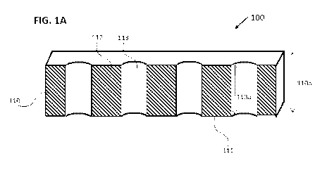
[0060] FIGS. 1-13, depict non-limiting example arrays for sorting particles.
FIG. 1A, is a
vertical slice through an array for sorting particles, in accordance with some
embodiments. Per
FIG. 1, the array 100 may comprise substrate 110 comprising a first surface
111 and a second
-7-
CA 03110219 2021-02-19
WO 2020/047508 PCT/US2019/049221
surface 112 opposite the first surface 111; a plurality of pores 113 extending
from the first
surface 111 to the second surface 112. The plurality of pores may be
substantially parallel to one
another and may be configured to hold the particles together with liquid. For
example, the liquid
can be held within the pores via surface tension, and can in some instances
form a meniscus.
[0061] Substrate 110 may comprise a substrate material. The substrate material
may be glass,
such as a silicate glass, fused silica, fused quartz, etc. The substrate
material may be a plastic,
such as PETG, PEEK, etc. The substrate may be a metal such as aluminum, steel,
chromium,
etc.
[0062] Substrate 110 may comprise a plurality of pores 113. In some cases, the
plurality of
pores 113 comprises about 1 hundred thousand to about 100 billion pores. In
some cases, the
plurality of pores 113 comprises about 1 thousand to about 1 billion pores. In
some cases, the
plurality of pores 113 comprises about 1 million to about 100 billion pores.
[0063] Substrate 110 may comprise a density of pores. The density of pores may
comprise the
number of pores per square millimeter of an array. The density of pores may be
measured at first
surface 111 or a second surface 112. Optionally, in some embodiments, the
first array 100 has
an open array fraction (packing density) of about 66 percent or from about 40
percent to about 75
percent. In some cases, the pore density may be within a range from 100 to
2500 pores per
square millimeter. In some cases, the pore density may be within a range from
500 to 1500
pores per square millimeter. A method of manufacturing a high pore density may
be by fusing
tubes, such as capillary tubes. The pore density may be varied by varying the
wall thickness and
central diameter of the tubes.
[0064] In one non-limiting example, the first array 110 has a width and length
of 10x10 inches,
respectively, and comprises 240 million pores 113 with a diameter of 15 um
each.
[0065] Additionally, the first array 100, per FIG. 1A, has an array height
110a measured as a
normal distance between the first surface 111 and the second surface 112. In
some embodiments,
the array height 110a can be measured as a maximum or a minimum normal
distance between
the first surface 111 and the second surface 112. In some embodiments, the
array height 110a
can be measured as a normal height of the pores 113. In some embodiments, the
array height
110a can be measured as a maximum or a minimum length of the pores 113. The
length may be
uniform between pores, or the pores may vary from pore to pore, such as via
distortion or
irregularity during the manufacturing processes. Optionally, each of the pores
113 has a length
of equal to or less than about 50 mm. In some cases, each pore may have a
length selected from
about 1 mm to about 500 mm. In some cases, each pore may have a length
selected from about
lmm to about 100 mm. In some cases, each pore may have a length selected from
about 1 mm
to about 10 mm.
-8-
CA 03110219 2021-02-19
WO 2020/047508 PCT/US2019/049221
[0066] Optionally the plurality of pores 113 may be orthogonal to the first
surface 111 and the
second surface 112. In some embodiments, the plurality of pores 113 can be
substantially
parallel to each other. In some embodiments, the first surface opposite the
second surfaces may
be substantially parallel planes. The plurality of pores may extend
orthogonally from the first
surface to the second surface. The pores may extend perpendicularly from the
first surface to the
second surface. Alternatively, the plurality of pores may extend at angle
relative to a surface
normal from the first surface to the second surface. The angle may be less
than 90 degrees from
normal. The angle may be less than 60 degrees, less than 45 degrees, less than
30 degrees, or
less. The angle may be within a range from 5 to ninety degrees.
[0067] In some embodiments, the plurality of pores may traverse an indirect
path from the first
surface to the second surface. In such embodiments, the pores may be tangled,
woven, or
interleaved. The pores may comprise one or a plurality of bends, such that a
path through the
pore substantially changes direction with respect to a direct route from the
first surface to the
second surface.
[0068] FIG. 1B is a top view of array 100 for sorting particles. In some
examples, array 100
has a plurality of pores 113. Each of the pores may comprise a cross-section.
The cross-section
may be circular, may be an oval, may be polyhedral (e.g. square, hexagon,
octagon, dodecagon,
etc.), or may have an irregular shape. The shape may be uniform between pores,
or the pores
may vary from pore to pore, such as via distortion or irregularity during the
manufacturing
processes.
[0069] The cross-section may comprise a largest cross-sectional dimension
113b. The largest
cross-sectional dimension may be measured at either of the two surfaces of the
array or at an
intermediate position. The largest cross-sectional dimension may be measured
at a single cross-
section. Additionally or alternatively, the largest cross-sectional dimension
may be averaged
across many positions along the pore. The dimension may be measured in many
ways, such as
under a microscope using a reference, by interferometer, calculated from flow,
etc. In some
examples, each pore of the array may comprise a cross-sectional dimension
within a range from
microns to 100 microns. In some examples, each pore may have a cross-sectional
dimension
within a range from 15 microns to 50 microns.
[0070] In some cases, the largest cross-sectional dimension may be a diameter.
The term
diameter is intended to encompass the largest cross-sectional distance across
a pore which is
round, approximately round, or an oval. In some examples, each pore of the
array may comprise
a pore diameter within a range from 5 microns to 100 microns. In some
examples, each pore may
have a diameter within a range from 10 microns to 50 microns.
-9-
CA 03110219 2021-02-19
WO 2020/047508 PCT/US2019/049221
[0071] Each pore 113 may comprise a cross-sectional area. The cross-sectional
area may be
measured at a single cross-section. Additionally or alternatively, the cross-
sectional area may be
averaged across many positions along the pore. The white region of pore 113
shown in FIG. 1B
may define a cross-sectional area at first surface of a pore. Optionally, each
of the micropores
113 has a cross sectional area equal to or less than about one square
millimeter. In some cases,
each pore of the plurality of pores may have a largest cross-sectional area of
about 0.008 mm2 or
less.
[0072] Each pore 113 of the array may comprise an aspect ratio. The aspect
ratio may be the
fraction of the length of the pore over the largest cross-sectional dimension
of the pore. The
aspect ratio may be the fraction of the length of the pore over the diameter
of the pore. In some
cases, the aspect ratio may be within a range from 10 to 100. In some cases,
the aspect ratio may
be 10 or greater. In some cases, the aspect ratio may be 20 or greater. In
some cases, the aspect
ratio may be 100 or greater.
[0073] FIG. 1C shows an example image of arrays with different cell
concentrations. Each
well may comprise one or a plurality of particles of interest, such as a cell,
as shown in the
illustrated embodiment. The one or a plurality of particles may comprise one
or a plurality of
cells. A number of a plurality of cells may be about 1, about 5, about 25, or
more. In some
examples, a number of a plurality of cells may be less than about 100 or less
than about 1000.
[0074] In some embodiments, an aqueous sample solution may be deposited onto
the array 100,
such as by spreading the aqueous sample solution onto the array 100. In some
embodiments, the
hydrophilic first surface 111 of the array 100 absorbs the aqueous sample
solution into the pores
113. In some embodiments, the first surface 111 of the array 100 distributes a
particle of interest,
such as a cell within the aqueous sample solution among the micropores 113. In
some
embodiments, the first surface 111 of the array 100 randomly distributes the
particle of interest
within the aqueous sample solution among the micropores 113. In some
embodiments, the
particle or particles of interest may settle at the bottom of each micropore
113. Optionally, in
some embodiments, the particle of interest may be withheld in each pore 113 by
the surface
tension of the aqueous sample solution.
[0075] The substrate material may be configured to be disrupted in response to
electromagnetic
radiation being directed at or adjacent to a portion of the substrate
material. Accordingly, once
particles of interest are identified as being held within a particular
microchannel of the array,
electromagnetic radiation may be directed at a first surface to disrupt the
substrate material,
which can result in the breaking of the meniscus of the liquid held in the
microchannel to release
the particle of interest. In certain embodiments, the electromagnetic
radiation removes, e.g.,
-10-
CA 03110219 2021-02-19
WO 2020/047508 PCT/US2019/049221
ablates, a portion of the substrate material in or adjacent to a pore in the
microarray, thereby
breaking the meniscus of the liquid held in the microchannel of the pore.
Surface Material
[0076] Provided herein is a non-limiting example of an array 100 comprising a
surface
material, shown in FIGS. 2-17B. The surface material 120 may comprise a
coating. The coating
can be coupled to first surface 111. In some embodiments, the surface material
may comprise a
material different from that of the substrate material. In one example, the
coating may comprise a
metal such as a transition metal, e.g., chromium. The surface material or
coating may be
configured to be disrupted from the first surface in response to
electromagnetic radiation being
directed at or adjacent to a portion of the surface material. Accordingly,
once particles of interest
are identified as being held within a particular microchannel of the array,
electromagnetic
radiation may be directed at a surface to disrupt and/or peel the coating,
which can break a
meniscus of the liquid held in the microchannel to release the particle of
interest.
[0077] FIG. 2A is a side cross-sectioned view of an example array for sorting
particles, in
accordance with some embodiments. As illustrated in FIG. 2A, the array 100 can
comprise a
substrate 110. The substrate can comprise a plurality of pores 113. The
substrate 110 can
comprise a second surface 112 and a first surface 111 opposite the second
surface 112.
Optionally, the plurality of pores 113 can extend from the first surface 111
to the second surface
112. In some embodiments, the coating 120 can be operably coupled to the first
surface 111.
[0078] In some embodiments, array 100 has an open array fraction (packing
density) of about 66
percent. In some embodiments, each of the pores 113 has a cross sectional area
equal to or less
than about one square millimeter. In some embodiments, each of the pores 113
has a diameter of
about 50 um to about 150 um. In some embodiments, each of the pores 113 has a
length of equal
to or less than about 50 mm. In some embodiments, the plurality of pores 113
are orthogonal to
the second surface 112 and the first surface 111. In some embodiments, each of
the pores 113 in
the plurality of pores 113 can be substantially parallel to each other. In
some embodiments, the
plurality of pores 113 comprises about 1 million to about 100 billion pores.
[0079] Additionally, the array 100, per FIG. 2A, has an array height 110a
measured as a
distance from the second surface 112 to the surface material 120. In some
embodiments, the
array height 110a may be measured as a normal distance between the first
surface 111 and the
second surface 112. In some embodiments, the array height 110a can be measured
as a
maximum or a minimum normal distance between the first surface 111 and the
second surface
112. In some embodiments, the array height 110a can be measured as a normal
height of the
pores 113. In some embodiments, the array height 110a can be measured as a
maximum or a
minimum height of the pores 113.
-11-
CA 03110219 2021-02-19
WO 2020/047508 PCT/US2019/049221
[0080] FIG. 2B is a top view of an example array in accordance with some
embodiments. The
plurality of pores 113, per FIG. 2B, within the array 100 are arranged in an
orthogonal pattern.
In some embodiments, the pattern comprises a linear pattern, a triangular
pattern, a hexagonal
pattern, an irregular pattern, or any combination thereof. The orthogonal
pattern of pores 113,
per FIG. 2B, has at least one of a first separation 113b and a second
separation 113c, wherein
the first separation 113b and a second separation are measured between the
center points of
consecutive pores 1513. In some embodiments, at least one of the first
separation 113b and a
second separation are measured as a normal distance between opposing points on
the surface of
consecutive pores 113. In some embodiments, at least one of the first
separation 113b and the
second separation 113c can be about 10 mm to about 40 mm.
[0081] An array described herein may comprise a coating 120. The coating can
be operably
coupled to the substrate. The coating can be configured to be disrupted when
subjected to
electromagnetic radiation. For example, in response to electromagnetic
radiation from a laser
being directed at a portion of the coating, the coating can chip or peel off.
Optionally, the coating
can comprise a material that is different from that of the substrate. For
example, the substrate
110 can comprise a first material and the coating 120 can comprise a second
material different
from the first material.
[0082] In some cases, the surface material may coat or partially coat the
second surface. In
additional or alternative cases, the surface material may coat or partially
coat the first surface. In
some cases, the surface material may not substantially block access to the
lumens of the pores.
However, blockage of some pores may occur, such as due to variations in
coating thickness
during manufacturing. The surface material may have an average thickness of
about 20
nanometers (nm) to 500 nm. The surface material may have an average thickness
of about 100
nm to 500 nm.
[0083] In some cases, the surface material may be substantially similar to the
substrate
material. In some instances, the array may be homogeneous. In some
embodiments, the
homogeneous array does not include a coating. In some embodiments, the
homogeneous array
comprises a uniform agglomeration or alloy material. In one example, the array
comprises a
metalloid, a transition metal, e.g., chromium, or both. In some embodiments,
the substrate
material comprises glass, plastic, aluminum, steel, stainless steel, or any
combination thereof
[0084] In some cases, the surface material may be substantially different than
the substrate
material. The substrate material may be glass and the surface material may be
a material other
than glass. In some cases, the surface material may comprise a metal. In some
case, the metal
may comprise chromium, silver, gold, aluminum etc. In some cases the surface
material may
comprise a metal oxide, such as magnesium fluoride, calcium fluoride, silicon
dioxide, etc. The
-12-
CA 03110219 2021-02-19
WO 2020/047508 PCT/US2019/049221
surface material may comprise layer of metals and/or metal oxides in order to
form tailored
optical properties such as reflection or absorption.
[0085] In some embodiments, the surface material comprises a transition metal,
e.g.,
chromium. In some embodiments, the second material comprises a metalloid. In
some
embodiments, the second material comprises a metal oxide. In some embodiments,
the second
material comprises Scandium, Titanium, Vanadium, Chromium, Manganese, Iron,
Cobalt,
Nickel, Copper, Zinc, Yttrium, Zirconium, Platinum, Gold, Mercury, Niobium,
Iridium,
Molybdenum, Silver, Cadmium, Tantalum, Tungsten, Aluminum, Silicon,
Phosphorous, Tin, an
oxide of any of the preceding or any combination thereof
[0086] In some embodiments, the surface material is selected from a material
which does not
negatively impact cell viability. For example, the surface material may be
biocompatible. The
surface material may be non-toxic. In certain embodiments, the surface
material is selected from
a material which when contacted with electromagnetic radiation does not cause
cell damage or
cell death. For example, products generated from contacting the surface
material with
electromagnetic radiation may themselves not cause cell damage or cell death.
That is, the
products generated, for example, by ablation of the surface material may be
biocompatible
and/or non-toxic to cells. In certain embodiments, impact on cell viability is
evaluated by
measuring cell viability prior to and after the cells are exposed to the
surface material. In certain
embodiments, the cell viability remains the same or decreases by less than
40%, less than 30%,
less than 20%, less than 15%, less than 10%, or even less than 5%. In certain
embodiments, cell
viability may be evaluated by measuring cell viability prior to and following
contacting the
surface material with the electromagnetic radiation. For example, the cell
viability is evaluated
prior to loading cells into the array and after the cells are released from
the pores of the array via
contacting the surface material with the electromagnetic radiation. In some
examples the
viability remains the same or decreases by less than 40%, less than 30%, less
than 20%, less than
15%, less than 10%, less than 5%, or even less than 1%, following contacting
the surface
material with the electromagnetic radiation.
[0087] The array can in some instances have a tailored hydrophobicity. In one
example, the
second surface 112 can be hydrophilic. Optionally, the second surface 112 need
not be
hydrophilic itself but can be operably coupled to a hydrophilic coating. In
some embodiments, a
portion of the coating 120 can be configured to be disrupted from the first
surface 111. In some
embodiments, a portion of the coating 120 can be configured to be disrupted
from the first
surface 111 in response to electromagnetic radiation being directed at the
portion of the coating.
In some embodiments, the coating 120 can be hydrophobic.
-13-
CA 03110219 2021-02-19
WO 2020/047508 PCT/US2019/049221
[0088] The coating can be configured to be disrupted in response to
electromagnetic radiation
being directed at a portion of the surface material. Accordingly, once
particles of interest are
identified as being held within a particular microchannel of the array,
electromagnetic radiation
can be directed at a coating to disrupt and/or peel the coating, which can
break a meniscus of the
liquid held in the microchannel to release the particle of interest. The
coating may absorb at a
wavelength or range of wavelengths which correspond to the wavelength emitted
by the source
of electromagnetic radiation.
[0089] Accordingly, once particles of interest are identified as being held
within a particular
pore of the array, electromagnetic radiation can be directed near or adjacent
to the particular pore
to release the particle of interest. In some embodiments, the disruption of
the second surface
comprises removing at least a portion of the material of the array, a coating
on the array, or both.
[0090] In some embodiments, disruption of the array may be caused by local
heating. Such a
mechanism may be likely when the pulse duration is longer, the peak power
density is lower,
and/or the wavelength of the incident radiation is in the infrared. Local
heating may cause
sublimation of the surface material or of the array material. In some
embodiments, the substrate
material and the coating comprise different thermal expansion coefficients,
which may lead to
chipping.
[0091] Additionally or alternatively, disruption of the array may be caused by
ablation. Such a
mechanism may be likely when the incident peak power density is higher, the
pulse duration is
shorter, the incident power is higher, and/or the incident radiation is in the
visible. Ablation may
comprise local bond breakage and/or vaporization of the array or substrate
material.
[0092] Additionally or alternatively, disruption of the array may be cause by
plasma
generation. This mechanism may be likely when the pulse duration of the
incident radiation is
especially short, the wavelength of the incident radiation is resonant with a
multi-photon
ionization mechanism, and or the wavelength of the incident radiation is very
short. Pulse
durations on the order of picoseconds to femtoseconds may yield faster plasma
generation than
local heating leading to optical etching of the substrate or surface mater.
[0093] Additionally or alternatively, disruption of the array may occur by
shock wave
generation. Such a mechanism may be more likely when the peak power density is
higher, a
phonon is resonant, and/or the pulse duration is shorter. Shock may cause
physical vibration,
chipping, or shaking of the surface or array material.
[0094] In an example, the surface material absorbs a range of wavelengths in
visible or
infrared. In some embodiments, the surface material may be opaque. The surface
material may
absorb at least a 5 nanometer band selected within a visible and infrared
range. The surface
material may absorb greater than 10 percent of incident radiation within an at
least 5 nanometer
-14-
CA 03110219 2021-02-19
WO 2020/047508 PCT/US2019/049221
band selected from 0.4 to 2.5 microns. The surface material may absorb greater
than 10 percent
of incident electromagnetic radiation of a wavelength selected from 0.4
microns to 2.5 microns.
In some cases, the surface material may absorb greater than 50 percent of
incident radiation
within an at least 5 nanometer band. The 5 nanometer band may be selected
within a range of
wavelengths from 0.4 to 2.5 microns. The surface material may absorb greater
than 50 percent
of incident electromagnetic radiation of a wavelength selected from 0.4
microns to 1.5 microns.
The surface material may absorb greater than 10 percent of incident radiation
at wavelength
selected from the harmonics of a doped Ytterbium Orthovanadate or Ytterbium
Aluminum
Garnet solid state laser. The surface material may absorb greater than 10
percent of incident
1064 nanometer radiation.
[0095] In one example, the coating e.g., a chromium coating, of an array has
an average
thickness of about 500 nm, which is reduced in thickness by an infrared (IR)
laser by about 100
nm or less, such as about 75 nm or less, or even about 50 nm or less. The
coating thickness may
be between 100 and 500 nm.
[0096] In some embodiments, the source of electromagnetic radiation may be
configured to
reduce the average thickness of the coating by about 1 nm to about 5 nm, by
about 1 nm to about
nm, by about 1 nm to about 20 nm, by about 1 nm to about 30 nm, by about 1 nm
to about 40
nm, by about 1 nm to about 60 nm, by about 1 nm to about 70 nm, by about 1 nm
to about 80
nm, by about 1 nm to about 90 nm, or by about 1 nm to about 100 nm.
[0097] In some embodiments, the source of electromagnetic radiation may be
configured to
ablate a portion of the array at an average depth of about 1 nm to about 5 nm,
of about 1 nm to
about 10 nm, of about 1 nm to about 20 nm, of about 1 nm to about 30 nm, of
about 1 nm to
about 40 nm, of about 1 nm to about 60 nm, of about 1 nm to about 70 nm, of
about 1 nm to
about 80 nm, of about 1 nm to about 90 nm, or by about 1 nm to about 100 nm.
[0098] In some embodiments, the source of electromagnetic radiation may be
configured to
remove a portion of the coating or of the array, the portion having a surface
area of about 11.tm2
to about 301.tm2, 11.tm2 to about 201.tm2, about 11.tm2 to about 101.tm2, or
about 11.tm2 to about 5
pin2.
[0099] In some embodiments, the source of electromagnetic radiation may be
configured to
ablate a portion of the array at an average distance from a circumference of
the micropore of
about 1 nm to about 5 nm, of about 1 nm to about 10 nm, of about 1 nm to about
20 nm, of about
1 nm to about 30 nm, of about 1 nm to about 40 nm, of about 1 nm to about 60
nm, of about 1
nm to about 70 nm, of about 1 nm to about 80 nm, of about 1 nm to about 90 nm,
or by about 1
nm to about 100 nm.
-15-
CA 03110219 2021-02-19
WO 2020/047508 PCT/US2019/049221
[0100] FIG. 3A shows a top view of an example array for sorting particles
comprising a
chrome coating, in accordance with some embodiments. FIG. 3B shows a top view
of a non-
limiting example array for sorting particles comprising a chrome coating
removed by a laser, in
accordance with some embodiments. Per FIGS. 3A-B, the coating 120 absorbs the
electromagnetic energy, which causes it to disrupt from the substrate 110,
which disturbs the
meniscus of the fluid within each pore 113 to eject the cells within. FIG. 3B,
shows pieces of the
coating 120 removed from the substrate 110 by the electromagnetic energy. As
seen in FIG. 3B,
the laser can be focused at or adjacent a single pore, between two adjacent
pores, or equidistant
from three pores. In some embodiments, focusing the infrared laser near a
single pore, between
two adjacent pores, or equidistant from three pores disturbs the meniscus of
the fluid within one,
two, or three pores 113, respectively, to eject the cells within. In some
embodiments, focusing
the laser closer to a specific pore decreases the likelihood of inadvertently
ejecting cells within
neighboring pores. In some embodiments, at least one of the intensity and
duration of the
infrared laser can be configured for controlled ejection of cells within one,
two, or three pores.
[0101] In some embodiments, the surface material 120 can be formed by
sputtering 100 nm
thick chrome on a glass array. In some embodiments, the sputtering can be
performed under a
vacuum. In some embodiments, the vacuum can be about 0.08 to about 0.02 mbar.
In some
embodiments, the sputtering can be performed under a voltage of about 100V to
3kV. In some
embodiments, the sputtering can be performed under a current: 0 to 50 mA.
Optionally, in some
embodiments, the chromium can be sputtered at only one side of the glass
array. In some
embodiments, the chromium coated array can be then soaked in a basic solution,
e.g., NaOH
solution. In some embodiments, the NaOH solution has a concentration of about
1 M. In some
embodiments, the chromium coated array can be soaked for a period of time of
about 12 hours.
In some embodiments, the chromium coated array can be then soaked in 10
percent bleach for up
to 1 hour, wherein a then water spray removes any residual bleach. In some
embodiments, the
chromium coated array can be then blow dried prior to loading cells.
[0102] In some embodiments, extraction of PBMC comprises adding a surfactant
and a
receiving media onto the chromium coated array; inserting the array can be
assembled into a
cassette with chromium coated side facing down, towards the receiving media;
dropping PBMC
on the array, and allowing the PBMC to settle into the pores. In some
embodiments, the
surfactant protects the integrity of the cell membrane and improves robustness
under liquid
shear. In some embodiments, the surfactant comprises a non-ionic surfactant.
In some
embodiments, the non-ionic surfactant comprises 0.1 percent of pluoronic F68.
In some
embodiments, the receiving media comprises OptiPEAK T Cell media. In some
embodiments,
-16-
CA 03110219 2021-02-19
WO 2020/047508 PCT/US2019/049221
the receiving media further comprises streptavidin. In some embodiments, the
PBMC are
allowed to settle into the micropores for a period of time of about 5 minutes.
[0103] In some embodiments, IR energy emitted from a laser and absorbed by the
chromium
coating may cause the coating to expand and delaminate at the bottom edges of
each micropore
to extracts the PBMC from each of the micropores. The separation of the
chromium coating at
the bottom edge of each micropore breaks the meniscus of the fluid therein to
release the PBMC.
[0104] FIG. 4A is a top view of IR energy absorbing fluorescent dye stained
PBMCs in a non-
limiting example first array comprising a chrome coating, in accordance with
some
embodiments. FIG. 4B is a top view of an example first array comprising a
chrome coating, after
extraction of the PBMCs, in accordance with some embodiments.
Beads
[0105] In certain embodiments, the pores of the arrays may comprise beads
which absorb
electromagnetic radiation and affect the breaking of a fluid miniscus in the
pores. In some cases,
the beard may be bound to the luminal surface of the pore or may be unbound
(added to the pore
in a liquid mixture). Provided herein is a bead comprising a core and a shell.
The beads of the
present disclosure may be referend to as "microspheres". The core may comprise
an infrared (IR)
absorbing core. The shell may comprise a non-IR absorbing shell. A bead of the
disclosure may
be associated with a pore of an array and the bead may absorb electromagnetic
radiation. The
non-IR absorbing shell may insulate the IR absorbing core from nearby
particles, e.g., cells,
thereby protecting the particles from damaging effects of the core with IR
absorbed radiation.
The bead may further comprise agarose. The non-IR absorbing shell may comprise
agarose. The
bead may further comprise dextran. The bead may be stained with an IR
absorbing dye. The
bead may comprise a diameter equal to or less than about 20 p.m, such as from
about 1 p.m to
about 20 p.m, or about 5 p.m to about 20 p.m. The bead may comprise an
absorbing shell which
may be equal to or less than about 10 microns. In some embodiments, the
surface material of an
array as described herein may comprise a bead comprising an infrared absorbing
core, and a non-
infrared absorbing shell, wherein an external diameter of the non-infrared
absorbing shell is
equal to or less than about 10 microns.
[0106] FIG. 5A shows array 100 comprising beads disposed therein. In some
cases, the beads
may be disposed on the interior of a lumen of a pore. In some cases, the beads
may be disposed
on a first surface 111. In some cases, the beads may be disposed within the
lumen of the pore.
FIG. 5B shows a side cross-sectioned view of an aqueous sample solution within
the example
array of FIG. 5A. In some embodiments, depositing the aqueous sample solution
521 onto the
array 100 comprises spreading the aqueous sample solution 521 onto the array
100. In some
embodiments, the hydrophilic first surface 111 of the array 100 absorbs the
aqueous sample
-17-
CA 03110219 2021-02-19
WO 2020/047508 PCT/US2019/049221
solution 521 into the pores 113. In some embodiments, the hydrophilic first
surface 111 of the
array 100 evenly distributes the first cells 522 and the second cells 523
within the aqueous
sample solution 521 among the pores 113. In some embodiments, the hydrophilic
first surface
111 of the array 100 randomly distributes the first cells 522 and the second
cells 523 within the
aqueous sample solution 521 among the pores 113. In some embodiments, the
first cells 522 and
the second cells 523 settle at the bottom of each pore 113. Optionally, in
some embodiments, the
first cells 522 and the second cells 523 are withheld in each pore 113 by the
surface tension of
the aqueous sample solution 521.
[0107] FIG. 6A shows a bright field image of the array of micropores filled
with microspheres
and cells, in accordance with some embodiments. As seen in FIG. 6A, each of
the micropores
601 within the array 600 can be occluded by the microbeads and the cells in
each respective the
micropores 601. FIG. 6B shows a bright field image of the extraction of a cell
from a single
micropore, in accordance with some embodiments. As seen in FIG. 6B, only one
micropore 601
within the array 600 cannot be occluded by the cells, indicating that only the
cells in the single
micropore 601 have been removed. FIG. 6C shows an image of the array of
micropores filled
with microspheres and one cells, in accordance with some embodiments. As seen
in FIG. 6C,
only one of the micropores 601 within the array 600 comprises a cell. FIG. 6D
shows an image
of the array 600 after the extraction of the cell from a single micropore, in
accordance with some
embodiments. As seen in FIG. 6D, none of the micropore 601 within the array
600 comprise a
cell, indicating that the single cell in the single micropore 601 has been
removed.
[0108] FIG. 7A shows an example bright field image of an extracted cell, in
accordance with
some embodiments. FIG. 7B shows an example image of an extracted cell, in
accordance with
some embodiments.
[0109] Provided herein, per FIGS. 8-13, are example beads or microspheres.
FIG. 8 shows a
bright field image of an example agarose and dextran microsphere. In some
embodiments, the
agarose and dextran microspheres 800 are configured to absorb infrared light.
In some
embodiments, the agarose and dextran microspheres 800 have are opaque, black,
or both. In
some embodiments, the agarose and dextran microspheres 800 comprise polymer
shell iron
oxide microspheres 800. In some embodiments, the agarose and dextran
microsphere 800 has a
diameter of about 6 um to about 20 um.
[0110] FIG. 9 shows a high magnification infrared image of the example agarose
and dextran
microsphere. As seen in FIG. 9, the agarose and dextran microsphere 800
comprises an infrared
(IR) absorbing core 910 and a non-IR absorbing shell 920. In some embodiments,
the IR
absorbing core 910 comprises an IR absorbing dye. In some embodiments, the IR
absorbing dye
-18-
CA 03110219 2021-02-19
WO 2020/047508 PCT/US2019/049221
comprises Epolight 1178. In some embodiments, the non-IR absorbing shell 920
comprises
agarose and dextran.
[0111] Employing an IR core dyed particle may be advantageous for efficient
cell extraction.
First, a dye integrated into the molecular structure of the agarose core may
increase IR
absorption more than a dye coating. Further, the non-IR absorbing soft shell
may act as a
buffering layer to protect cells from the stress and thermal shock associated
with any potential
absorbed heat, volume expansion, and/or micro-bubble formation. Both may allow
for increased
extraction efficiency (higher number of successful extraction events), and
high cell viability.
[0112] FIG. 10A shows a bright field image of an example agarose and IR dye
microsphere.
FIG. 10B shows an infrared image of an example agarose and IR dye microsphere.
As seen in
FIG. 10B, the agarose and IR dye microsphere 1000 can be infrared (IR)
absorbing. In some
embodiments, the agarose and IR dye microsphere 1000 comprises agarose. In
some
embodiments, the agarose and IR dye microsphere 1000 comprises an IR absorbing
dye. In some
embodiments, the IR absorbing dye comprises Epolight 1178. In some
embodiments, the dye
comprises green fluorescent protein. In some embodiments, the dye comprises
red fluorescent
protein. In some embodiments, the dye comprises a cyanine dye, an acridine
dye, a flourone dye,
an oxazine dye, a rhodomine dye, a coumarin dye, a pheanthridine dye, a BODIPY
dye, an
ALEXA dye, a perylene dye, an anthracene dye, a naphthaline dye, etc. In some
embodiments,
the agarose and IR dye microsphere 1000 has a diameter of about 2 p.m to about
16 p.m.
[0113] FIG. 11 shows an infrared image of an example microsphere comprising
chrome. FIG.
12 shows an infrared image of the example microsphere comprising chrome in an
example array.
FIG. 13 shows a high magnification infrared image of the example microsphere
comprising
chrome in a micropore. In some embodiments, the microsphere 1100 comprises a
transition
metal, e.g., chromium. Optionally, in some embodiments, the microsphere 1100
comprises a
chromium coating.
[0114] Provided herein is a method of forming an infrared absorbing bead. In
some
embodiments, the method comprises: washing Agarose beads; dying the Agarose
beads; and
forming the core of the Agarose beads. In some embodiments, washing Agarose
beads comprises
suspending the Agarose beads in a first solvent and centrifuging the Agarose
beads and the first
solvent. In some embodiments, the first solvent comprises an organic solvent,
e.g., acetone, or
aqueous solvent, e.g., water or a combination thereof In some embodiments, the
centrifuging
can be performed at a rate of about 1,000 rpm to about 4,000 rpm. In some
embodiments, the
centrifuging can be performed at a rate of about 2,000 rpm. In some
embodiments, 1 mL of the
first solvent can be used for every 50 mg of the Agarose beads. In some
embodiments, the
Agarose beads comprise Superdex beads.
-19-
CA 03110219 2021-02-19
WO 2020/047508 PCT/US2019/049221
[0115] In some embodiments, dying the Agarose beads comprises forming a dying
solution,
centrifuging the dying solution, and adding the dying solution to the Agarose
beads. The dying
solution may comprise Epolin 1178 and a second solvent. In some embodiments,
the second
solvent comprises acetone, water, deionized water, or any combination thereof.
The centrifuging
may be performed at a rate of about 2,000 rpm to about 10,000 rpm, e.g., about
5,000 rpm. In
some embodiments, dying the Agarose beads further comprises incubating the
Agarose beads
and the dying solution. The incubation may be performed for about 15 minutes
to about 1 hour,
e.g., about 30 minutes. In some embodiments, the incubation can be performed
at room
temperature. The incubation may be performed with constant mixing. In some
embodiments,
dying the Agarose beads further comprises centrifuging the Agarose beads after
incubation, e.g.,
at a rate of about 750 rpm to about 3,000 rpm. In some embodiments, dying the
Agarose beads
further comprises separating the dark beads from the light beads. In some
embodiments, dying
the Agarose beads further comprises suspending the Agarose beads in 0.2
percent BSA-PBS.
[0116] In some embodiments, forming the core of the Agarose beads comprises
suspending the
Agarose beads in a third solvent and centrifuging the Agarose beads and the
third solvent. In
some embodiments, the third solvent comprises a 1:1 acetone-water mixture. In
some
embodiments, the centrifuging can be performed at a rate of about 500 rpm to
about 2,000 rpm.
In some embodiments, the centrifuging can be performed for about 10 seconds to
about 60
seconds.
[0117] Alternatively, in some embodiments forming the core of the Agarose
beads comprises
incubating the beads in a buffer. In some embodiments, the buffer comprises
BSA-PBS. In some
embodiments, the buffer has a concentration of about 0.2 percent. In some
embodiments,
incubating the beads in a buffer can be performed at a temperature of about 4
C. In some
embodiments, incubating the beads in a buffer can be performed for a period of
time of at least
about 5 days. Forming the core of the Agarose beads may further comprise
changing the buffer
each day.
[0118] Provide herein is a solution comprising a plurality of beads as
described herein and a
particle of interest as described herein. In some cases, the particle of
interest is a cell. In some
cases, the solution comprises a ratio of a number of the plurality of beads to
a number of a
plurality of cells, which is about 1:1 to 10:1. The solution comprising the
particle of interest may
be inserted into one or a plurality of pores of an array as described herein.
Example solutions are
described further with respect to examples five and six.
System
[0119] Another aspect provided herein is a system for sorting particles.
Provided herein is a
system for sorting components of a mixture. The system may comprise any
embodiment,
-20-
CA 03110219 2021-02-19
WO 2020/047508 PCT/US2019/049221
variation, or example of the array as described herein.
[0120] FIG. 14A, shows a system comprising array 100, a housing 1431, and an
internal
surface 1432. The system for sorting particles may comprise an array 100
comprising: a
substrate 110 comprising: a first surface 111; a second surface 112 opposite
the first surface 111;
and a plurality of pores 113 extending from the first surface 111 to the
second surface 112, each
of the pores 113 comprising a cross sectional area equal to or less than about
one square
millimeter and a length equal to or less than about 10 mm, wherein the
substrate 110 comprises a
first material; and a coating 120 operably coupled to the second surface 112,
wherein the coating
120 comprises a second material different from the first material, and wherein
a portion of the
coating 120 can be configured to be disrupted from the second surface 112 in
response to
electromagnetic radiation being directed at the portion of the coating 120;
and a fluid within the
plurality of pores 113 of the array 100, wherein a meniscus of fluid within
the plurality of pores
113 are substantially adjacent the coating 120.
[0121] In some embodiments, the first surface 111 can be hydrophilic. In some
embodiments,
the first surface 111 can be operably coupled to a hydrophilic coating 120. In
some
embodiments, the coating 120 can be hydrophobic. In some embodiments, the
coating 120 can
be capable of preventing leakage from the pores for a period equal to or
greater than 1 hour. In
some embodiments, the coating 120 covers the second surface 112 in its
entirety.
[0122] In some embodiments, the second material can be chromium. In some
embodiments, the
second material comprises silver, gold, aluminum, titanium, copper, platinum,
nickel, or cobalt.
In some embodiments, the first material can be glass. In some embodiments, the
cross sectional
area can be equal to or less than about 0.03 mm2. In some embodiments, the
length can be equal
to or less than about 1.5 mm. In some embodiments, the coating 120 comprises a
thickness equal
to or less than about 200 nm. In some embodiments, the substrate 110 comprises
a surface area
to volume ratio of about 0.5 m4. In some embodiments, the portion of the
coating 120 can be
configured to absorb the electromagnetic radiation and break off from the
second surface 112 in
response to electromagnetic radiation being directed at the portion of the
coating 120. In some
embodiments, the plurality of micropores 113 is orthogonal to the first
surface 111 and the
second surface 112. In some embodiments, the plurality of micropores 113 is
substantially
parallel to each other. In some embodiments, the plurality of micropores 113
is from about 1
million to about 100 billion micropores 113. In some embodiments, the second
material is
opaque. The second material may be configured to absorb infrared (IR) energy.
The substrate
110 and the coating 120 may comprise different thermal expansion coefficients.
[0123] Optionally, the system may additional comprise a housing 1431
comprising an internal
surface 1432 configured to receive selected contents released from the array.
The system may
-21-
CA 03110219 2021-02-19
WO 2020/047508 PCT/US2019/049221
comprise any embodiment, variation, or example of the array as described
herein and a housing
comprising an internal surface. The internal surface may be positioned below
the second surface
of the substrate. The system may additionally comprise a cell sorter. The
array be mounted on
the cell sorter.
[0124] Optionally, the system for sorting particles may comprise a source of
electromagnetic
radiation.
[0125] FIG. 14B shows a system for sorting particles comprising an array 100 a
source of
electromagnetic radiation 1451. The array can be configured to be disrupted at
the first surface or
the second surface in response to electromagnetic radiation being directed at
a portion of the first
or the second surface. In some instances, it can be beneficial for sorting
systems to be able to
release particles held in a particular compartment of an array without
directing lasers or other
energy sources directly at the compartment holding the particles of interest,
e.g., for helping
increase cell viability when the particles of interest are cells. Focusing the
laser energy at the
surface of the array rather than the interior of a pore in the array may
avoid, or reduce, possible
damage to the pore contents from thermal shock, thermal expansion, micro-
bubble generation,
and localized sheer stress.
[0126] The source of generating electromagnetic radiation may comprise a
laser. The laser
may be a doped solid state laser. The laser may be a fiber laser. The laser
may be a
semiconductor diode laser. The laser may be a gas laser, such as a HeNe laser
or an eximer laser.
The laser may emit electromagnetic radiation within a range of wavelengths. In
some
embodiments, the electromagnetic radiation may be emitted in the visible
and/or infrared. The
electromagnetic radiation may be emitted within a 5 nanometer band with then
visible or
infrared. The electromagnetic radiation may be emitted at a harmonic of a
doped solid state laser
such as doped Ytterbium Orthovanadate or Ytterbium Aluminum Garnet. The
electromagnetic
radiation may comprise 1064 nm radiation.
[0127] The electromagnetic radiation may comprise an incident energy. The
incident energy
may be greater than 0.1 microJoules per pulse. The incident energy may be less
than 1 milliJoule
per pulse. The incident energy may be within a range from 1 picoJoule to 1
Joule per pulse. The
average power may be less than 10 Watts. The average power may be less than
100 milli Watts.
The average power may be greater than 1 microWatt.
[0128] The electromagnetic radiation may comprise an incident peak power
density. The peak
power density may be less than 10 Terawatt per centimeter squared. The peak
power may be
less than 10 GigaWatts per centimeter squared.
[0129] The electromagnetic radiation may comprise an incident spot diameter.
The spot
diameter may be sufficiently small such that an area adjacent the pore may be
irradiated without
-22-
CA 03110219 2021-02-19
WO 2020/047508 PCT/US2019/049221
significantly irradiating the contents of the cell. The spot diameter may be
adjusted based on the
size of the pores and the pore spacing. The spot diameter may be sufficiently
small that an
interior wall of the pore lumen may be irradiated without significant
irradiation of the pore
contents, such as a cell in the interior of the lumen. The spot diameter may
be less than 10
millimeter (mm), less than 1 mm, less than 100 micron (1.tm), less than 10 tm,
or less.
[0130] The electromagnetic radiation may comprise an incident pulse duration.
The pulse
duration may be greater than about 5 femtoseconds. The pulse duration may be
greater than
about 100 femtoseconds. The pulse duration may be greater than about one
nanosecond or more.
The pulse duration may be less than about 1 microsecond.
[0131] An example source of electromagnetic radiation comprises a 1064nm,
Ytterbium fiber
laser, with a power of 0.1 mJ, a power density of 108-109 W/mm2, whereby a
spot diameter 20
1.tm at 10 percent-30 percent of maximum laser power with a 4 ns pulse
duration is capable of
providing 30-90 J/ cm2 to the array.
[0132] The system may additionally comprise one or a plurality of lenses for
focusing a source
of electromagnetic radiation. The one or a plurality of lenses may comprise a
microscope
objective. The microscope objective may be raster scanned across the surface
of the array in
order to target a particular portion of the array. The system may comprise one
or more
translation stages which may control the positioning of the objective relative
to the surface of the
array.
[0133] The system may comprise one or more beam splitters, filters, or
dichroic filters. The
system the one or more beam splitter, filters, or dichroic filters may allow
for a user to monitor
the surface of the array while aligning or direct a source of electromagnetic
radiation toward a
surface of the array. The alignment may be done a lower power electromagnetic
radiation than
would disrupt the array or at the same power. The system may comprise one or
more position
sensitive optical detectors, such as a CCD, in order to monitor an alignment
of the source of
electromagnetic radiation.
[0134] The system may comprise a second source of electromagnetic radiation.
The second
source of electromagnetic radiation may be used for alignment. The second
source of
electromagnetic radiation may be used to excite an absorber, such as a
fluorophore. The second
source of electromagnetic radiation may be coherent or incoherent. The second
source of
electromagnetic radiation may be broad band or narrow band. The second source
of
electromagnetic radiation may comprise any property described herein with
respect to a source
of electromagnetic radiation, such as power, pulse duration, wavelength, etc.
[0135] FIG. 15A and FIG. 15B show an example system 1400 comprising an array
and a
housing. FIG. 15A is a top initial view of a leak test at 0 hours. FIG. 18B is
a top initial view of
-23-
CA 03110219 2021-02-19
WO 2020/047508 PCT/US2019/049221
a leak test of an example array at 5 hours. Per FIG. 15A to FIG. 15B, a leak
test of an example
array 100 in a frame 1510 was performed with deionized water over a period of
about 5 hours,
wherein none of the deionized water leaked through the micropores of the
array. In some
embodiments, the coating of the example array 100 can be capable of preventing
leakage from
the pores for a period equal to or greater than about 1 hour. In some
embodiments, the coating of
the example array 100 can be capable of preventing leakage from the pores for
a period equal to
or greater than about 1 hour, 2 hours, 3, hours, 4 hours, 5, hours, 6 hours, 7
hours, 8 hours, 9
hours, or 10 hours.
Methods
[0136] The embodiments, examples, and variations of an array described herein
can be utilized
in a method for releasing particles from a pore of the array. The embodiments,
examples, and
variations of a system described herein can be utilized in a method for
releasing particles from a
pore of the array. Provided herein is a method of releasing particles from a
pore of an array, the
method comprising: filling the pore, holding the portion of the solution in
the pore, directing
electromagnetic radiation at a portion of the array, disrupting the portion of
the array, and
releasing the portion of the solution comprising the particle of interest. The
pore can be filled
with at least a portion of a solution. The solution can comprise a particle of
interest. The portion
of the solution can be held in the pore via surface tension. Disrupting the
portion of the array can
disrupt the surface tension of the portion of the solution held in the pore.
[0137] Provided herein is a method of releasing selected contents from a pore
of an array, the
method comprising: identifying a pore of an array with selected contents,
wherein the array
comprises a substrate with a first surface and a second surface opposite the
first surface, wherein
the substrate comprises a substrate material and a surface material wherein
the surface material is
positioned at or adjacent to the first or second surfaces, and the substrate
comprises a plurality of
pores defining lumens extending from the first surface to the second surface,
wherein the
substrate is characterized by one or more of: (a) each pore of the plurality
of pores has a largest
diameter of 500 microns or less, (b) each pore of the plurality of pores has
an aspect ratio of 10
or greater, (c) a pore density of 100 or greater pores per square millimeter,
and (d) the surface
material is selected from a material that absorbs greater than 10 percent of
incident
electromagnetic radiation, and removing a portion of the surface material from
the first or second
surface of the array with electromagnetic radiation directed to the surface
material within or
adjacent to the identified pore, thereby releasing the contents of the
identified pore.
[0138] In some examples, the array may be characterized by two or more of: (a)
each pore of
the plurality of pores has a largest diameter of 500 microns or less, (b) each
pore of the plurality
of pores has an aspect ratio of 10 or greater, (c) a pore density of 100 or
greater pores per square
-24-
CA 03110219 2021-02-19
WO 2020/047508 PCT/US2019/049221
millimeter, and (d) the surface material is selected from a material that
absorbs greater than 10
percent of incident electromagnetic radiation.
[0139] FIGS. 16A-E show a side cross-sectional views of an example method of
sorting cells
with an example array of FIG. 1, as described herein. Per FIGS. 16A-E, the
example method
1600 of sorting cells with the example first array 100 comprises: providing
1610 an array 100
comprising a plurality of pores 113. In some embodiment, the operation 1610
may further
comprise covering a portion of the pores 113 closest to the first surface 111
of the array 100
with microspheres, per FIG. 5A. An operation 1620 of the method 1600 may
comprise
depositing an aqueous solution 1621 within the array. In some cases, the array
may comprise
depositing a first cell 1622 and a second cell 1623 onto the first array 100,
per FIG. 16B. An
operation 1630 of the method 1600 may comprise inserting the array 100 within
a housing 1631,
per FIG. 16C. In some cases, the housing may comprise a cartridge. The housing
may comprise
and internal surface 1632. An operation 1640 of the method 100 may comprise
capturing a plot
of the signal the selected particles. The selected particles may comprise
first cells 1622 and
second cells 1623, per FIG. 16D. The method 1600 may further comprise locating
1640 a plot of
the signal of first cells 1622 within the plot of the signal of first cells
and the second cells 1623,
per FIG. 16E. The method 1600 may further comprise extracting 1640 the second
cell 1623
from the array 100; and collecting 1650 the second cell 1623 per FIG. 16F. The
step of
extracting the cell from the array may comprise disrupting a coating on at or
near the surface of
the array 100. The step of disrupting may comprise providing electromagnetic
radiation to the
surface of the array at selected location. FIG. 16A shows a side cross-
sectioned view of
providing an array comprising a plurality of pores comprising a coating, per
the example
method.
[0140] FIG. 16B shows a side cross-sectioned view of the depositing of an
aqueous sample
solution within the example array of FIG. 1. In some embodiments, depositing
1620 the aqueous
sample solution 1621 onto the array 100 comprises spreading the aqueous sample
solution 1621
onto the array 100. In some embodiments, the hydrophilic first surface 111 of
the array 100
absorbs the aqueous sample solution 1621 into the pores 113. In some
embodiments, the
hydrophilic first surface 111 of the array 100 evenly distributes the first
cells 1622 and the
second cells 1623 within the aqueous sample solution 1621 among the pores 113.
In some
embodiments, the hydrophilic first surface 111 of the array 100 randomly
distributes the first
cells 1622 and the second cells 1623 within the aqueous sample solution 1621
among the pores
113. In some embodiments, the first cells 1622 and the second cells 1623
settle at the bottom of
each pore 113. Optionally, in some embodiments, the first cells 1622 and the
second cells 1623
are withheld in each pore 113 by the surface tension of the aqueous sample
solution 1621. In
-25-
CA 03110219 2021-02-19
WO 2020/047508 PCT/US2019/049221
some examples, the cells are selected from INKT cells, Tmem, Treg, HSPCs, and
combinations
thereof.
[0141] FIG. 16C shows a side cross-sectioned view of inserting the example
array of FIG. 1
within a closed cartridge or housing, in accordance with some embodiments. Per
FIG. 16C, the
cartridge 1631 comprises a humidification membrane 1633 on top of the array
100 and a
collection tray 1632 to collect the second cell 1623. Optionally, in some
embodiments, the
cartridge 1631 comprises a closed cartridge 1631. Optionally, in some
embodiments, the
cartridge 1631 comprises a humidity controlled cartridge 1631. Optionally, in
some
embodiments, the humidification membrane 1633 reduces evaporation from the
pores 113.
Optionally, in some embodiments, the collection tray 1632 can be placed below
the array 100
within the cartridge 1631. Optionally, in some embodiments, the collection
tray 1632 comprises
a transparent collection tray 1632.
[0142] FIG. 16D shows an image of plots of the signal of first cells and the
second cells, in
accordance with some embodiments. Per FIG. 16D, a plot 1641 of the signal of
the second cells
can be determined. In some embodiments, the plot of the signal of first cells
1642 can be
determined. In some embodiments, the plots can be captured by quantifying an
image taken by
an automated fluorescent scanning system. The first cells may be fluorescent
at a first
wavelength and the second cells may be fluorescent at a second wavelength. In
some
embodiments, a combined image may be determined. FIG. 17 shows an example non-
limiting
raw fluorescent image of an array of cells. FIG. 18 shows an example non-
limiting scatter plot
0.5 million micropores of the array as represented in FIG. 17.
[0143] FIG. 16E shows a side cross-sectioned view of extracting the second
cells, in
accordance with some embodiments. Per, FIG. 16E, the second cells 1623 are
extracted from the
array 100 by exposing the pores 113 that, per the plot of the signal of the
second cells 1623 in
FIG. 16D, comprise the second cells 1623 to a pulse by a laser 1651. The laser
excites the
coating which may comprise microspheres within a specific pore 113.
Optionally, in some
embodiments, the laser 1651 comprises a nanosecond laser 1651.
[0144] FIG. 16F shows a side cross-sectioned view of collecting the cells, in
accordance with
some embodiments. Per, FIG. 16F, the second cells 1623 extracted from the
array 100 by the
laser 1651 may be collected in the collection tray 1661.
[0145] Another aspect provided herein is a method of releasing particles from
a pore of an
array, the method comprising: filling the pore with at least a portion of a
solution, wherein the
portion of the solution comprises a particle of interest; holding the portion
of the solution in the
pore via surface tension; directing electromagnetic radiation at a portion of
the array; disrupting
the portion of the array, thereby disrupting the surface tension of the
portion of the solution held
-26-
CA 03110219 2021-02-19
WO 2020/047508 PCT/US2019/049221
in the pore; and releasing the portion of the solution comprising the particle
of interest. In some
embodiments, the array comprises a substrate and a coating operably coupled to
the substrate. In
some embodiments, the substrate comprises a first surface, a second surface
opposite the first
surface, and the pore, wherein the pore extends from the first surface to the
second surface. In
some embodiments, the first surface is hydrophilic, and the coating is
hydrophobic. In some
embodiments, the portion of the array is a coating of the array. In some
embodiments, the portion
of the array is a coating of the array proximate the pore. In some
embodiments, the coating
comprises chromium. In some embodiments, the array comprises a plurality of
pores. In some
embodiments, the method further comprises filling the plurality of pores with
the solution. In
some embodiments, the method further comprises releasing solutions held in a
subset of the
plurality of pores, wherein the subset of the plurality of pores hold
solutions comprising the
particle of interest. The method may further comprise analyzing a plurality of
fluorescent
signatures for each of the particles. In some embodiments, the method further
comprises
determining the pore holding the portion of the solution comprising the
particle of interest based
on the analysis. In some embodiments, the particles are released at a rate of
about 5,000 to about
100,000,000 particles of interest per second. In some embodiments, the
particle of interest
comprises a cell. In some embodiments, the cell is released with viability
equal to or greater than
60 percent. In some embodiments, the method further comprises receiving the
particle of interest
in a housing, wherein the housing comprises an internal surface to receive the
particle of interest.
In some embodiments, the internal surface holds a receiving media. In some
embodiments, the
receiving media comprises pluoronic F68.
[0146] In some embodiments, the method further comprises removing a portion of
the surface
material from the first or second surface of the array with electromagnetic
radiation directed to
the surface material within or adjacent to the identified pore, thereby
releasing the contents of the
identified pore. In some examples, the portion of the surface material may be
adjacent to the
identified pore. The portion of the surface may comprise a luminal surface of
the identified pore.
The portion of the surface may be removed to a depth of 100 microns or less.
The portion of the
surface may be removed to a depth of 50 microns or less.
[0147] In some cases, the step of loading the array with a solution comprising
the selected
contents prior to the identifying the pore with selected contents. In some
cases, the step of
identifying the pore with selected contents comprises analyzing emitted
electromagnetic
radiation from the pores of the array. In some case, the step of releasing the
contents comprises
releasing the contents at a rate of about 5,000 to about 100,000,000 pores per
second.
[0148] The source of generating electromagnetic radiation may comprise a
laser. The laser
may be a doped solid state laser. The laser may be a fiber laser. The laser
may be a
-27-
CA 03110219 2021-02-19
WO 2020/047508 PCT/US2019/049221
semiconductor diode laser. The laser may be a gas laser, such as a HeNe laser
or an eximer laser.
The laser may emit electromagnetic radiation within a range of wavelengths. In
some
embodiments, the electromagnetic radiation may be emitted in the visible
and/or infrared. The
electromagnetic radiation may be emitted within a 5 nanometer band with then
visible or
infrared. The electromagnetic radiation may be emitted at a harmonic of a
doped solid state laser
such as doped Ytterbium Orthovanadate or Ytterbium Aluminum Garnet. The
electromagnetic
radiation may comprise 1064 nm radiation.
[0149] The electromagnetic radiation may be selected from a wavelength of 0.2
microns to 2.5
microns, and a fluence level sufficient to disrupt adhesion between the
contents and the pore, and
a pulse duration in a range from 1 ns to 1 millisecond.
[0150] Accordingly, once particles of interest are identified as being held
within a particular
pore of the array, electromagnetic radiation can be directed near or adjacent
to the particular pore
to release the particle of interest. In some embodiments, the disruption of
the second surface
comprises removing at least a portion of the material of the array, a coating
on the array, or both.
[0151] In some embodiments, the step of removing a portion of the surface
material may be
caused by local heating. Such a mechanism may be likely when the pulse
duration is longer, the
peak power density is lower, and/or the wavelength of the incident radiation
is in the infrared.
Local heating may cause sublimation of the surface material or of the array
material. In some
embodiments, the substrate material and the coating comprise different thermal
expansion
coefficients, which may lead to chipping.
[0152] In some cases, the step of removing a portion of the surface material
may be caused by
ablation. Such a mechanism may be likely when the incident peak power density
is higher, the
pulse duration is shorter, the incident power is higher, and/or the incident
radiation is in the
visible. Ablation may comprise local bond breakage and/or vaporization of the
array or substrate
material.
[0153] In some cases, the step of removing a portion of the surface material
may be cause by
plasma generation. This mechanism may be likely when the pulse duration of the
incident
radiation is especially short, the wavelength of the incident radiation is
resonant with a multi-
photon ionization mechanism, and or the wavelength of the incident radiation
is very short.
Pulse durations on the order of picoseconds to femtoseconds may yield faster
plasma generation
than local heating leading to optical etching of the substrate or surface
mater.
[0154] In some cases, the step of removing a portion of the surface material
may occur by
shock wave generation. Such a mechanism may be more likely when the peak power
density is
higher, a phonon is resonant, and/or the pulse duration is shorter. Shock may
cause physical
vibration, chipping, or shaking of the surface or array material.
-28-
CA 03110219 2021-02-19
WO 2020/047508 PCT/US2019/049221
[0155] In some cases, the step of removing a portion of the surface material
photochemical
removal, such as photoionization. In some cases, the step of removing a
portion of the surface
material comprises photoacoustic removal, such as by optical generation of a
shock wave.
Terms and Definitions
[0156] Unless otherwise defined, all technical terms used herein have the same
meaning as
commonly understood by one of ordinary skill in the art to which this
disclosure belongs.
[0157] As used herein, the singular forms "a," "an," and "the" include plural
references unless
the context clearly dictates otherwise. Any reference to "or" herein is
intended to encompass
"and/or" unless otherwise stated.
[0158] As used herein, the term "about" refers to an amount that is near the
stated amount by
percent, 5 percent, or 1 percent, including increments therein.
[0159] As used herein, the term "PBMC" refers to a peripheral blood
mononuclear cell.
[0160] As used herein, the term "orthogonal" refers to a perpendicular
arrangement or
relationship.
EXAMPLES
[0161] The following illustrative examples are representative of embodiments
of the software
applications, systems, and methods described herein and are not meant to be
limiting in any way.
Example 1 ¨ Chromium Coated Micropore Array Preparation:
[0162] Glass micropore array purchased from Income Inc. (C00113, 3005722, 20
[tm pore, 60
percent pore coverage) was sputtered with 100 nm thick chrome at LGA thin
films (Santa Clara,
CA, vacuum: 8 x10⁻² to 2 x10⁻² mbar, sputtering voltage: 100V to 3kV, current:
0 to 50 mA).
The chromium was sputtered at only one side of the pore plate. Afterwards, the
chromium coated
micropore array was first soaked with 1 M NaOH solution for 12 hours, 10
percent bleach for up
to 1 hour, and then water sprayed to remove any residual bleach and blow dried
prior to loading
cells.
Example 2 ¨ Cassette assembly:
[0163] The cassette includes (from top to bottom): a glass sealed to the top
of the cassette; an
aluminum alloy frame to hold the micropore plate; a receiving glass plate
which was spaced at
consistent or variable distances from the micropore plate. Receiving media
(OptiPEAK T Cell
media, InVitria, Junction City, KS) with 0.1 percent pluoronic F68 (Cat.
24040032,
ThermoFisher Scientific Inc.) of different volume (depending on the cassette
size) was added
into the receiving plate. The chromium coated micropore array was assembled
into the cassette
-29-
CA 03110219 2021-02-19
WO 2020/047508 PCT/US2019/049221
with chromium coated side facing down (facing the receiving media). Pluoronic
F68 addition to
receiving media can greatly increase the viability of cells extracted from
pores from 0 percent
viability to >75 percent viability.
Example 3 ¨ Cell Sorting With Chromium Coated Micropore Array:
[0164] PBMCs with density 2 million/ mL in OptiPEAK T Cell media were dropped
on top of
the micropore array and allowed to settle for 5 mins for single cells to be
captured at the bottom
of the micropores by surface tension. Afterwards, the cassette was mounted on
the cell sorter. A
laser power from 10-100 percent can be used to extract cells from the
micropores. Chromium
coating at the edges of micropore bottom absorbed IR laser energy and a thin
layer of chromium
was removed. The meniscus was broken and cells were released from the desired
micropores.
Example 4 ¨ Manufacture of Agarose Beads with IR Absorbing Core:
[0165] This procedure describes the preparation of agarose beads with a
transparent shell and
IR absorbing core.
[0166] Step 1. Suspend 50 mg Superdex beads (Superdex 75 100/300 GL, GE
Healthcare Life
Sciences) into 1 mL acetone. Centrifuge at 2000 rpm to collect Superdex beads.
Discard acetone.
Make saturated IR absorbing dye (Epolight 1178, Epolin, New Jersey, USA)
solution 1 mL in
acetone. Centrifuge at 5000 rpm to remove any un-dissolved IR dye. Add IR dye
solution into
Superdex beads. Incubate at room temperature with constant mixing for 30 mins.
Centrifuge the
mixture at 1500 rpm. Discard the top liquid. Only save the dark pellet at the
bottom. Without
further washing by acetone, suspend the resulted dark pellet into 0.2 percent
BSA-PBS. This
results in uniformly IR dye incorporated Superdex beads.
[0167] Step 2. To remove dye from the external portion of the beads, in less
than 15 seconds,
rinse beads in a 1:1 acetone-water mixture by pipetting. Immediately after,
centrifuge the
mixture at 1000 rpm for 30 sec, and discard the top liquid. This will result
in the IR core
structure.
[0168] Alternatively, the IR absorbing core can be made by incubating the
beads from Step 1 in
0.2 percent BSA-PBS at 4 degree for >5 days. Change buffer 1 time each day.
This will slowly
dissolve the IR dye from the Superdex beads via molecule diffusion only.
[0169] The efficacy of the IR dye microspheres are shown in Table 1, below.
-30-
CA 03110219 2021-02-19
WO 2020/047508 PCT/US2019/049221
Extraction % %Viability
Bead type Efficiency (%) (multiple cells) (Single
cells)
Control
(IR dye coated TiO2 bead) 4 48 0
Agarose and dextran 24 27 73
microsphere
Agarose and IR dye 51 72 N/A
microsphere
[0170] The efficacy of the chrome microspheres is shown in Table 2, below.
Extraction
Bead type (Cells/mm2) % Viability
IR Dye Stained Bead #1 52 105
IR Dye Stained Bead #2 10 131
Chrome Coated Bead 9 0
Example 5 ¨ Single PBMC Viability with Pluronic F68 as Media Supplement:
[0171] The procedure describes a media supplement for enhancing cell viability
during cell
sorting.
Cells were suspended and harvested in OptiPEAK T Lymphocyte Complete Media
(7770PT069) supplemented with 0.1 percent pluronic F68 and 1X
penicillin/streptomycin for
cell loading and harvesting. In this example, percent viability for each of
three samples was
measured as, 81 percent, 74 percent, and 65 percent, respectively, for an
example array with a 20
1.tm micropore size.
Example 6 ¨PBMC Extraction:
[0172] This procedure describes a solution comprising a particle of interest
and a bead.
[0173] A solution containing human PBMC cells was dropped on top of the
micropore array.
After 10 mins, single PBMCs were loading into the micropores. Afterwards,
solutions containing
either control beads (IR dye coated TiO2 beads), or agarose and dextran beads,
or agarose and IR
dye microspheres were loaded on top of the micropore array. After 15- 30 mins,
beads were
loaded into micropores by gravity. The pore array with cells and beads were
mounted on top of
receiving reservoir containing cell culture media. IR pulsed laser was
directed to target the
-31-
CA 03110219 2021-02-19
WO 2020/047508 PCT/US2019/049221
bottom of the pore where beads were loaded, and cells were extracted into the
cell culture media.
After extraction, cell culture media containing extracted cells was harvested
for viability assay.
Example 7 ¨ Cell Viability:
[0174] This procedure describes determining cell viability.
[0175] Cell viability was determined by quantitative sandwich ELISA assay
(Human IFN-
gamma ELISpot Kit, R&D Systems Inc., No. EL285). The assay employs a capture
antibody
specific for human cytokine interferon y (IFN-gamma), pre-coated onto a PVDF-
backed
microplate. Harvested cells were pipetted directly into the wells and the
immobilized antibody in
the immediate vicinity of the secreting cells binds secreted human IFN-gamma.
Following wash
steps and incubation with a biotinylated detection antibody, alkaline-
phosphatase conjugated to
streptavidin was added. Unbound enzyme was subsequently removed by washing and
a substrate
solution was added. A blue colored precipitate may form at the sites of
cytokine and appeared as
spots, with each individual spot representing an individual human IFN-gamma
secreting cell.
The spots were counted. Standard cell samples of serial dilution with known
viable cell numbers
were also plated the same way as the harvested cell samples. By counting the
blue spots in each
well, standard curve was plotted. The number of viable cells in harvested
samples was
determined by the standard curve.
[0176] While preferred embodiments of the present invention have been shown
and described
herein, it will be obvious to those skilled in the art that such embodiments
are provided by way
of example only. Numerous variations, changes, and substitutions will now
occur to those
skilled in the art without departing from the invention. It should be
understood that various
alternatives to the embodiments of the invention described herein may be
employed in practicing
the invention.
-32-