Note : Les descriptions sont présentées dans la langue officielle dans laquelle elles ont été soumises.
CA 03112333 2021-03-09
WO 2020/056339 PCT/US2019/051129
METHODS FOR ASSAYING BINDING AFFINITY
[0001] This application claims the benefit of priority of U.S. Provisional
Patent Application No.
62/731,123, filed September 14, 2018, the content of which is incorporated
herein by reference
for its entirety.
INTRODUCTION AND SUMMARY
[0002] Scientists have long been interested in measuring the binding affinity
between molecules
that specifically interact with one another. For protein therapeutics, surface
plasmon resonance
(SPR) has become the most widely accepted technique for determining binding
affinities.
However, SPR requires costly equipment that is exclusively dedicated to the
measurement of
binding affinity and requires a large amount of highly purified material.
Given these drawbacks
to SPR, which limits its use to only a limited number of candidate molecules,
there is a need for
new approaches to the measurement of binding affinity that require less
preparatory work and
can be performed at larger scale.
[0003] The present disclosure provides methods for assaying a binding affinity
between a first
molecule and a second molecule. The micro-fluidic device comprises a flow
region and a
chamber that opens off of the flow region.
[0004] In some embodiments, the methods comprise: providing the second
molecule into the
chamber, wherein the second molecule is labeled with a signal-emitting moiety
and a first
capture micro-object comprising the first molecule is present in the chamber;
removing unbound
second molecule from the microfluidic device; providing a second capture micro-
object into the
chamber, wherein the second capture micro-object comprises a third molecule
which specifically
binds to the second molecule; detecting over a period of time a decrease in an
amount of second
molecule bound to the first capture micro-object; and determining a relative
binding affinity
between the first molecule and the second molecule.
[0005] In some embodiments, providing the second molecule into the chamber
further comprises
allowing the second molecule to bind to the first molecule of the first
capture micro-object. In
some embodiments, the binding of the second molecule to the first molecule is
allowed to
proceed to saturation. In some embodiments, the methods further comprise
detecting over the
period of time an increase in the amount of second molecule bound to the
second capture micro-
obj ect.
1
CA 03112333 2021-03-09
WO 2020/056339 PCT/US2019/051129
[0006] In some embodiments, the binding affinity between the first molecule
and the second
molecule is determined based on one of the following: the decrease in the
amount of second
molecule bound to the first capture micro-object over the period of time, or a
ratio of (i) the
increase in the amount of second molecule bound to the second capture micro-
object over the
period of time to (ii) the decrease in the amount of second molecule bound to
the first capture
micro-object over the period of time.
[0007] In certain embodiments, the methods comprise: providing a second
molecule labeled with
a signal-emitting moiety into the chamber, wherein a first capture micro-
object comprising the
first molecule is present in the chamber; removing unbound second molecule
from the
microfluidic device; detecting over a period of time a decrease in the amount
of the second
molecule bound to the first capture micro-object; and determining a relative
binding affinity
between the first molecule and the second molecule.
[0008] In some embodiments, providing a second molecule labeled with a signal-
emitting
moiety into the chamber further comprises allowing the second molecule to bind
to the first
molecule of the first capture micro-object. In some embodiments, the binding
of the second
molecule to the first molecule is allowed to proceed to saturation. In some
embodiments, the
binding affinity between the first molecule and the second molecule is
determined based on the
decrease in amount of second molecule bound to the first capture micro-object
over the period of
time.
[0009] In certain embodiments, methods for assaying binding affinities of a
target molecule and
each of a plurality of distinct binding partners in a micro-fluidic device are
provided. The micro-
fluidic device comprises a flow region and a plurality of chambers that open
off of the flow
region. In certain embodiments, the methods comprise: providing the target
molecule into the
plurality of chambers, wherein the target molecule is labeled with a signal-
emitting moiety and
wherein a first plurality of capture micro-objects, each comprising a distinct
binding partner, are
present in the plurality of chambers; removing unbound target molecule from
the microfluidic
device; providing a second plurality of capture micro-objects into the
plurality of chambers,
wherein each of the capture micro-objects of the second plurality comprises a
binding partner for
the target molecule; detecting over a period of time a decrease in the amount
of target molecule
bound to the capture micro-objects of the first plurality; determining
relative binding affinities of
the target molecule and each of the plurality of distinct binding partners.
2
CA 03112333 2021-03-09
WO 2020/056339 PCT/US2019/051129
[0010] In some embodiments, providing the target molecule into the plurality
of chambers
further comprises allowing the target molecule to bind to the binding partners
of the capture
micro-objects of the first plurality. In some embodiments, the binding of the
target molecule to
the binding partners is allowed to proceed to saturation. In some embodiments,
the methods
further comprise detecting over the period of time an increase in the amount
of target molecule
bound to the capture micro-objects of the second plurality.
[0011] In some embodiments, the relative binding affinities between the target
molecule and
each of the plurality of distinct binding partners are determined based on (1)
decreases in the
amount of target molecule bound to the capture micro-objects of the first
plurality over the
period of time, or (2) ratios of (i) increases in the amount of target
molecule bound to the capture
micro-objects of the second plurality over the period of time to (ii)
decreases in the amount of
target molecule bound to the capture micro-objects of the first plurality over
the period of time.
[0012] In certain embodiments, methods for assaying binding affinities of a
target molecule and
one or more binding partners for the target molecule in a micro-fluidic device
are provided. The
micro-fluidic device comprises a flow region and a chamber that opens off of
the flow region. In
certain embodiments, the methods comprise: providing the target molecule into
the chamber,
wherein the target molecule is labeled with a signal-emitting moiety and
wherein a first capture
micro-object comprising a first binding partner is present in the chamber;
removing unbound
target molecule from the microfluidic device; providing a second capture micro-
object into the
chamber, wherein the second capture micro-object comprises a second binding
partner different
from the first binding partner; detecting over a period of time a decrease in
the amount of target
molecule bound to the first capture micro-object; determining a relative
binding affinity of the
target molecule and the first binding partner.
[0013] In some embodiments, providing the target molecule into the chamber
further comprises
allowing the target molecule to bind to the first binding partner of the first
capture micro-object,
wherein the binding of the target molecule to the first binding partner is
allowed to proceed to
saturation. In some embodiments, the methods further comprise detecting over
the period of time
an increase in the amount of target molecule bound to the second capture micro-
object.
[0014] In some embodiments, the relative binding affinity of the target
molecule and the first
binding partner is determined based on (1) the decrease in the amount of
target molecule bound
to the first capture micro-object over the period of time, or (2) a ratio of
(i) the increase in the
3
CA 03112333 2021-03-09
WO 2020/056339 PCT/US2019/051129
amount of target molecule bound to the second capture micro-object over the
period of time to
(ii) the decrease in the amount of target molecule bound to the first capture
micro-object over the
period of time.
[0015] These and other features and advantages of the disclosed methods will
be set forth or will
become more fully apparent in the description that follows and in the appended
claims. The
features and advantages may be realized and obtained by means of the objects
and combinations
particularly pointed out in the appended examples, partial listing of
embodiments, and claims.
Furthermore, the features and advantages of the described methods may be
learned by the
practice or will be obvious from the description, as set forth hereinafter.
BRIEF DESCRIPTION OF THE DRAWINGS
[0016] Figure 1A illustrates an example of a system for use with a
microfluidic device and
associated control equipment according to some embodiments of the disclosure.
[0017] Figures 1B and 1C illustrate a microfluidic device according to some
embodiments of the
disclosure.
[0018] Figures 2A and 2B illustrate isolation pens according to some
embodiments of the
disclosure.
[0019] Figure 2C illustrates a detailed sequestration pen according to some
embodiments of the
disclosure.
[0020] Figures 2D-2G illustrate sequestration pens according to some other
embodiments of the
disclosure.
[0021] Figure 2H illustrates a microfluidic device according to an embodiment
of the disclosure.
[0022] Figure 3 illustrates a coated surface of the microfluidic device
according to an
embodiment of the disclosure.
[0023] Figure 4A illustrates a specific example of a system for use with a
microfluidic device
and associated control equipment according to some embodiments of the
disclosure.
[0024] Figure 4B illustrates an imaging device according to some embodiments
of the
disclosure.
[0025] Figures 5A-5B illustrate exemplary structural parameters of an
exemplary microfluidic
device as well as adjustable parameters that can be configured for the assay,
according to some
embodiments of the disclosure, according to some embodiments of the
disclosure. Figure 5A
shows an embodiment with a single first capture micro-object and a single
second capture micro-
4
CA 03112333 2021-03-09
WO 2020/056339 PCT/US2019/051129
object; Figure 5B shows an embodiment having a single first capture micro-
object and a plurality
of second capture micro-objects.
[0026] Figures 5C-5D illustrate exemplary structural parameters of an
exemplary microfluidic
device as well as adjustable parameters that can be configured for the assay,
according to some
embodiments of the disclosure.
[0027] Figure 6A illustrates a kinetic rate model illustrating transition
rates in the source-capture
assay. One capture bead and one source bead are shown, but the model can be
generalized to
multiple capture beads and one source, multiple source and one capture, or
multiple capture and
multiple source beads.
[0028] Figure 6B illustrates an expected change in fluorescence intensity of
first and second
capture micro-objects according to some embodiments of the disclosure.
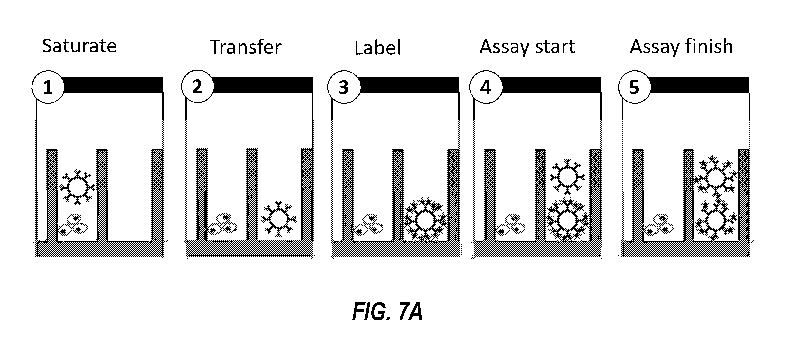
[0029] Figure 7A illustrates steps of a method for performing a binding
affinity assay between a
first micro-object and a second micro-object, according to some embodiments of
the disclosure.
[0030] Figure 7B illustrates a method for performing the assay on an array of
molecules with
differing binding affinities, according to some embodiments of the disclosure.
[0031] Figure 8A illustrates the use of first and second capture micro-objects
to assay binding
affinity between a first molecule and a second molecule according to some
embodiments of the
disclosure.
[0032] Figures 8B-8C provide images of a microfluidic device in which first
and second capture
micro-objects are being used to assay binding affinity between a first
molecule and a second
molecule according to some embodiments of the disclosure.
[0033] Figure 8D provides graphical displays of the change in the ratio of
fluorescent intensity
of the second capture micro-object to the first capture micro-object over time
according to some
embodiments of the disclosure.
[0034] Figures 8E-8G show relative assessments of binding affinity which
relies upon the use of
first and second capture micro-objects to assay binding affinity between a
first molecule and a
second molecule according to some embodiments of the disclosure.
[0035] Figures 9A-9C illustrate a method for performing the assay on an array
of molecules with
differing binding affinities, according to some embodiments of the disclosure.
CA 03112333 2021-03-09
WO 2020/056339 PCT/US2019/051129
DETAILED DESCRIPTION
[0036] This specification describes exemplary embodiments and applications of
the disclosure.
The disclosure, however, is not limited to these exemplary embodiments and
applications or to
the manner in which the exemplary embodiments and applications operate or are
described
herein. Moreover, the figures may show simplified or partial views, and the
dimensions of
elements in the figures may be exaggerated or otherwise not in proportion. In
addition, as the
terms "on", "attached to," "connected to," "coupled to," or similar words are
used herein, one
element (e.g., a material, a layer, a substrate, etc.) can be "on," "attached
to," "connected to," or
"coupled to" another element regardless of whether the one element is directly
on, attached to,
connected to, or coupled to the other element or there are one or more
intervening elements
between the one element and the other element. Also, unless the context
dictates otherwise,
directions (e.g., above, below, top, bottom, side, up, down, under, over,
upper, lower, horizontal,
vertical, "x," "y," "z," etc.), if provided, are relative and provided solely
by way of example and
for ease of illustration and discussion and not by way of limitation. In
addition, where reference
is made to a list of elements (e.g., elements a, b, c), such reference is
intended to include any one
of the listed elements by itself, any combination of less than all of the
listed elements, and/or a
combination of all of the listed elements. Section divisions in the
specification are for ease of
review only and do not limit any combination of elements discussed.
[0037] Where dimensions of microfluidic features are described as having a
width or an area, the
dimension typically is described relative to an x-axial and/or y-axial
dimension, both of which lie
within a plane that is parallel to the substrate and/or cover of the
microfluidic device. The height
of a microfluidic feature may be described relative to a z-axial direction,
which is perpendicular
to a plane that is parallel to the substrate and/or cover of the microfluidic
device. In some
instances, a cross sectional area of a microfluidic feature, such as a channel
or a passageway,
may be in reference to a x-axial/z-axial, a y-axial/z-axial, or an x-axial/y-
axial area.
I. Definitions
[0038] As used herein, "substantially" means sufficient to work for the
intended purpose. The
term "substantially" thus allows for minor, insignificant variations from an
absolute or perfect
state, dimension, measurement, result, or the like such as would be expected
by a person of
ordinary skill in the field but that do not appreciably affect overall
performance. In some
6
CA 03112333 2021-03-09
WO 2020/056339 PCT/US2019/051129
embodiments, when used with respect to numerical values or parameters or
characteristics that
can be expressed as numerical values, "substantially" means within ten
percent.
[0039] Numeric ranges are inclusive of the numbers defining the range.
[0040] "Or" is used in the inclusive sense, i.e., equivalent to "and/or,"
unless the context requires
otherwise.
[0041] The term "ones" means more than one.
[0042] As used herein, the term "plurality" can be 2, 3, 4, 5, 6, 7, 8, 9, 10,
or more.
[0043] As used herein: [tm means micrometer, [tm3 means cubic micrometer, pL
means
picoliter, nL means nanoliter, and [IL (or uL) means microliter.
[0044] As used herein, the term "disposed" encompasses within its meaning
"located."
[0045] As used herein, a "microfluidic device" or "microfluidic apparatus" is
a device that
includes one or more discrete microfluidic circuits configured to hold a
fluid, each microfluidic
circuit comprised of fluidically interconnected circuit elements, including
but not limited to
region(s), flow path(s), channel(s), chamber(s), and/or pen(s), and at least
one port configured to
allow the fluid (and, optionally, micro-objects suspended in the fluid) to
flow into and/or out of
the microfluidic device. Typically, a microfluidic circuit of a microfluidic
device will include a
flow region, which may include a microfluidic channel, and at least one
chamber, and will hold a
volume of fluid of less than about 1 mL, e.g., less than about 750, 500, 250,
200, 150, 100, 75,
50, 25, 20, 15, 10, 9, 8, 7, 6, 5, 4, 3, or 2 L. In certain embodiments, the
microfluidic circuit
holds about 1-2, 1-3, 1-4, 1-5, 2-5, 2-8, 2-10, 2-12, 2-15, 2-20, 5-20, 5-30,
5-40, 5-50, 10-50, 10-
75, 10-100, 20-100, 20-150, 20-200, 50-200, 50-250, or 50-300 L. The
microfluidic circuit
may be configured to have a first end fluidically connected with a first port
(e.g., an inlet) in the
microfluidic device and a second end fluidically connected with a second port
(e.g., an outlet) in
the microfluidic device.
[0046] As used herein, a "nanofluidic device" or "nanofluidic apparatus" is a
type of
microfluidic device having a microfluidic circuit that contains at least one
circuit element
configured to hold a volume of fluid of less than about 1 [tL, e.g., less than
about 750, 500, 250,
200, 150, 100, 75, 50, 25, 20, 15, 10, 9, 8, 7, 6, 5, 4, 3, 2, 1 nL or less. A
nanofluidic device may
comprise a plurality of circuit elements (e.g., at least 2, 3, 4, 5, 6, 7, 8,
9, 10, 15, 20, 25, 50, 75,
100, 150, 200, 250, 300, 400, 500, 600, 700, 800, 900, 1000, 1500, 2000, 2500,
3000, 3500,
4000, 4500, 5000, 6000, 7000, 8000, 9000, 10,000, or more). In certain
embodiments, one or
7
CA 03112333 2021-03-09
WO 2020/056339 PCT/US2019/051129
more (e.g., all) of the at least one circuit elements is configured to hold a
volume of fluid of
about 100 pL to 1 nL, 100 pL to 2 nL, 100 pL to 5 nL, 250 pL to 2 nL, 250 pL
to 5 nL, 250 pL to
nL, 500 pL to 5 nL, 500 pL to 10 nL, 500 pL to 15 nL, 750 pL to 10 nL, 750 pL
to 15 nL, 750
pL to 20 nL, 1 to 10 nL, 1 to 15 nL, 1 to 20 nL, 1 to 25 nL, or 1 to 50 nL. In
other embodiments,
one or more (e.g., all) of the at least one circuit elements are configured to
hold a volume of fluid
of about 20 nL to 200nL, 100 to 200 nL, 100 to 300 nL, 100 to 400 nL, 100 to
500 nL, 200 to
300 nL, 200 to 400 nL, 200 to 500 nL, 200 to 600 nL, 200 to 700 nL, 250 to 400
nL, 250 to 500
nL, 250 to 600 nL, or 250 to 750 nL.
[0047] A microfluidic device or a nanofluidic device may be referred to herein
as a "microfluidic
chip" or a "chip"; or "nanofluidic chip" or "chip".
[0048] A "microfluidic channel" or "flow channel" as used herein refers to
flow region of a
microfluidic device having a length that is significantly longer than both the
horizontal and
vertical dimensions. For example, the flow channel can be at least 5 times the
length of either
the horizontal or vertical dimension, e.g., at least 10 times the length, at
least 25 times the length,
at least 100 times the length, at least 200 times the length, at least 500
times the length, at least
1,000 times the length, at least 5,000 times the length, or longer. In some
embodiments, the
length of a flow channel is about 100,000 microns to about 500,000 microns,
including any value
therebetween. In some embodiments, the horizontal dimension is about 100
microns to about
1000 microns (e.g., about 150 to about 500 microns) and the vertical dimension
is about 25
microns to about 200 microns, (e.g., from about 40 to about 150 microns). It
is noted that a flow
channel may have a variety of different spatial configurations in a
microfluidic device, and thus
is not restricted to a perfectly linear element. For example, a flow channel
may be, or include
one or more sections having, the following configurations: curve, bend,
spiral, incline, decline,
fork (e.g., multiple different flow paths), and any combination thereof. In
addition, a flow
channel may have different cross-sectional areas along its path, widening and
constricting to
provide a desired fluid flow therein. The flow channel may include valves, and
the valves may
be of any type known in the art of microfluidics. Examples of microfluidic
channels that include
valves are disclosed in U.S. Patents 6,408,878 and 9,227,200, each of which is
herein
incorporated by reference in its entirety.
[0049] As used herein, the term "obstruction" refers generally to a bump or
similar type of
structure that is sufficiently large so as to partially (but not completely)
impede movement of
8
CA 03112333 2021-03-09
WO 2020/056339 PCT/US2019/051129
target micro-objects between two different regions or circuit elements in a
microfluidic device.
The two different regions/circuit elements can be, for example, the connection
region and the
isolation region of a microfluidic sequestration pen.
[0050] As used herein, the term "constriction" refers generally to a narrowing
of a width of a
circuit element (or an interface between two circuit elements) in a
microfluidic device. The
constriction can be located, for example, at the interface between the
isolation region and the
connection region of a microfluidic sequestration pen of the instant
disclosure.
[0051] As used herein, the term "transparent" refers to a material which
allows visible light to
pass through without substantially altering the light as is passes through.
[0052] As used herein, the term "saturation" refers to the state where target
molecules bind to
substantially all of the target-specific binding partners available on a
capture micro-object(s) in a
same chamber or sequestration pen.
[0053] As used herein, the term "micro-object" refers generally to any
microscopic object that
may be isolated and/or manipulated in accordance with the present disclosure.
Non-limiting
examples of micro-objects include: inanimate micro-objects such as
microparticles; microbeads
(e.g., polystyrene beads, LuminexTM beads, or the like); magnetic beads;
microrods; microwires;
quantum dots, and the like; biological micro-objects such as cells; biological
organelles; vesicles,
or complexes; synthetic vesicles; liposomes (e.g., synthetic or derived from
membrane
preparations); lipid nanorafts (as described, for example, in Ritchie et al.
(2009) "Reconstitution
of Membrane Proteins in Phospholipid Bilayer Nanodiscs," Methods Enzymol.,
464:211-231),
and the like; or a combination of inanimate micro-objects and biological micro-
objects (e.g.,
microbeads attached to cells, liposome-coated micro-beads, liposome-coated
magnetic beads, or
the like). Beads may include moieties/molecules covalently or non-covalently
attached, such as
fluorescent labels, nucleic acids (e.g., oligonucleotides), proteins,
carbohydrates, antigens, small
molecule signaling moieties, or other chemical/biological species capable of
use in an assay.
[0054] As used herein, a "distance" between the micro-objects is measured
between the center of
the micro-objects.
[0055] As used herein, the term "cell" is used interchangeably with the term
"biological cell."
Non-limiting examples of biological cells include eukaryotic cells, plant
cells, animal cells, such
as mammalian cells, reptilian cells, avian cells, fish cells, or the like,
prokaryotic cells, bacterial
cells, fungal cells, protozoan cells, or the like, cells dissociated from a
tissue, such as muscle,
9
CA 03112333 2021-03-09
WO 2020/056339 PCT/US2019/051129
cartilage, fat, skin, liver, lung, neural tissue, and the like, immunological
cells, such as T cells, B
cells, natural killer cells, macrophages, and the like, embryos (e.g.,
zygotes), oocytes, ova, sperm
cells, hybridomas, cultured cells, cells from a cell line, cancer cells,
infected cells, transfected
and/or transformed cells, reporter cells, and the like. A mammalian cell can
be, for example,
from a human, a mouse, a rat, a horse, a goat, a sheep, a cow, a primate, or
the like.
[0056] A colony of biological cells is "clonal" if all of the living cells in
the colony that are
capable of reproducing are daughter cells derived from a single parent cell.
In certain
embodiments, all the daughter cells in a clonal colony are derived from the
single parent cell by
no more than 10 divisions. In other embodiments, all the daughter cells in a
clonal colony are
derived from the single parent cell by no more than 14 divisions. In other
embodiments, all the
daughter cells in a clonal colony are derived from the single parent cell by
no more than 17
divisions. In other embodiments, all the daughter cells in a clonal colony are
derived from the
single parent cell by no more than 20 divisions. The term "clonal cells"
refers to cells of the
same clonal colony.
[0057] As used herein, a "colony" of biological cells refers to 2 or more
cells (e.g. about 2 to
about 20, about 4 to about 40, about 6 to about 60, about 8 to about 80, about
10 to about 100,
about 20 to about 200, about 40 to about 400, about 60 to about 600, about 80
to about 800,
about 100 to about 1000, or greater than 1000 cells).
[0058] As used herein, the term "maintaining (a) cell(s)" refers to providing
an environment
comprising both fluidic and gaseous components and, optionally a surface, that
provides the
conditions necessary to keep the cells viable and/or expanding.
[0059] As used herein, the term "expanding" when referring to cells, refers to
increasing in cell
number.
[0060] A "component" of a fluidic medium is any chemical or biochemical
molecule present in
the medium, including solvent molecules, ions, small molecules, antibiotics,
nucleotides and
nucleosides, nucleic acids, amino acids, peptides, proteins, sugars,
carbohydrates, lipids, fatty
acids, cholesterol, metabolites, or the like.
[0061] As used herein, "capture moiety" is a chemical or biological species,
functionality, or
motif that provides a recognition site for a micro-object. A selected class of
micro-objects may
recognize the in situ-generated capture moiety and may bind or have an
affinity for the in situ-
CA 03112333 2021-03-09
WO 2020/056339 PCT/US2019/051129
generated capture moiety. Non-limiting examples include antigens, antibodies,
and cell surface
binding motifs.
[0062] As used herein, the term "signal-emitting moiety" (also known as a
label) assists the user
by enabling detection of a molecule (e.g., target or target-specific binding
partner) to which it
binds directly or indirectly. When the disclosure refers to detecting a
molecule (or an amount or
change in amount thereof), the disclosure references detecting the signal
produced by the signal-
emitting moiety bound to the molecule. Various optical or non-optical signal-
emitting moieties
may be employed for signaling purposes. In some embodiments, the signal-
emitting moiety is
optically observable. In some embodiments, the signal-emitting moiety is a
signal emitting
molecule that fluoresce may be used, such as organic small molecules,
including, but not limited
to fluorophores, such as, but not limited to, fluorescein, Texas Red,
Rhodamine, cyanine dyes,
Alexa dyes, DyLight dyes, Atto dyes, etc. In some embodiments, organic
polymers, such as p-
dots may be employed. In some embodiments, the signal-emitting moiety may be a
biological
molecule, including but not limited to a fluorescent protein or fluorescent
nucleic acid. In some
embodiments, the signal-emitting moiety may be an inorganic moiety including Q-
dots. In some
embodiments, the signal-emitting moiety may be a moiety that operates through
scattering, either
elastic or inelastic scattering, such as nanoparticles and Surface Enhanced
Raman Spectroscopy
(SERS) reporters (e.g., 4- Mercaptobenzoic acid, 2,7-mercapto-4-
methylcoumarin). In some
embodiments, the signal-emitting moiety may be
chemiluminescence/electrochemiluminescence
emitters such as ruthenium complexes and luciferases. In some embodiments, the
signal-emitting
moiety generates an optical signal or an electromagnetic signal (across the
entire electromagnetic
spectrum).
[0063] As used herein, "flowable polymer" is a polymer monomer or macromer
that is soluble or
dispersible within a fluidic medium (e.g., a pre-polymer solution). The
flowable polymer may be
input into a microfluidic flow region and flow with other components of a
fluidic medium
therein.
[0064] As used herein, "photoinitiated polymer" refers to a polymer (or a
monomeric molecule
that can be used to generate the polymer) that upon exposure to light, is
capable of crosslinking
covalently, forming specific covalent bonds, changing regiochemistry around a
rigidified
chemical motif, or forming ion pairs which cause a change in physical state,
and thereby forming
a polymer network. In some instances, a photoinitiated polymer may include a
polymer segment
11
CA 03112333 2021-03-09
WO 2020/056339 PCT/US2019/051129
bound to one or more chemical moieties capable of crosslinking covalently,
forming specific
covalent bonds, changing regiochemistry around a rigidified chemical motif, or
forming ion pairs
which cause a change in physical state. In some instances, a photoinitiated
polymer may require
a photoactivatable radical initiator to initiate formation of the polymer
network (e.g., via
polymerization of the polymer).
[0065] As used herein, "antibody" refers to an immunoglobulin (Ig) and
includes both
polyclonal and monoclonal antibodies; primatized (e.g., humanized); murine;
mouse-human;
mouse-primate; and chimeric; and may be an intact molecule, a fragment thereof
(such as scFv,
Fv, Fd, Fab, Fab' and F(ab)'2 fragments), or multimers or aggregates of intact
molecules and/or
fragments; and may occur in nature or be produced, e.g., by immunization,
synthesis or genetic
engineering. An "antibody fragment," as used herein, refers to fragments,
derived from or
related to an antibody, which bind antigen and which in some embodiments may
be derivatized
to exhibit structural features that facilitate clearance and uptake, e.g., by
the incorporation of
galactose residues. This includes, e.g., F(ab), F(ab)'2, scFv, light chain
variable region (VL),
heavy chain variable region (VH), and combinations thereof.
[0066] As used herein in reference to a fluidic medium, "diffuse" and
"diffusion" refer to
thermodynamic movement of a component of the fluidic medium down a
concentration gradient.
[0067] The phrase "flow of a medium" means bulk movement of a fluidic medium
primarily due
to any mechanism other than diffusion. For example, flow of a medium can
involve movement
of the fluidic medium from one point to another point due to a pressure
differential between the
points. Such flow can include a continuous, pulsed, periodic, random,
intermittent, or
reciprocating flow of the liquid, or any combination thereof. When one fluidic
medium flows
into another fluidic medium, turbulence and mixing of the media can result.
[0068] The phrase "substantially no flow" refers to a rate of flow of a
fluidic medium that,
averaged over time, is less than the rate of diffusion of components of a
material (e.g., an analyte
of interest) into or within the fluidic medium. The rate of diffusion of
components of such a
material can depend on, for example, temperature, the size of the components,
and the strength
of interactions between the components and the fluidic medium.
[0069] As used herein in reference to different regions within a microfluidic
device, the phrase
"fluidically connected" means that, when the different regions are
substantially filled with fluid,
such as fluidic media, the fluid in each of the regions is connected so as to
form a single body of
12
CA 03112333 2021-03-09
WO 2020/056339 PCT/US2019/051129
fluid. This does not mean that the fluids (or fluidic media) in the different
regions are
necessarily identical in composition. Rather, the fluids in different
fluidically connected regions
of a microfluidic device can have different compositions (e.g., different
concentrations of
solutes, such as proteins, carbohydrates, ions, or other molecules) which are
in flux as solutes
move down their respective concentration gradients and/or fluids flow through
the microfluidic
device.
[0070] As used herein, a "flow path" refers to one or more fluidically
connected circuit elements
(e.g. channel(s), region(s), chamber(s) and the like) that define, and are
subject to, the trajectory
of a flow of medium. A flow path is thus an example of a swept region of a
microfluidic device.
Other circuit elements (e.g., unswept regions) may be fluidically connected
with the circuit
elements that comprise the flow path without being subject to the flow of
medium in the flow
path.
[0071] As used herein, "isolating a micro-object" confines a micro-object to a
defined area
within the microfluidic device.
[0072] As used herein, an "isolation region" refers to a region within a
microfluidic device that
is configured to hold a micro-object such that the micro-object is not drawn
away from the
region as a result of fluid flowing through the microfluidic device. Depending
upon context, the
term "isolation region" can further refer to the structures that define the
region, which can
include a base/substrate, walls (e.g., made from microfluidic circuit
material), and a cover.
[0073] A microfluidic (or nanofluidic) device can comprise "swept" regions and
"unswept"
regions. As used herein, a "swept" region is comprised of one or more
fluidically interconnected
circuit elements of a microfluidic circuit, each of which experiences a flow
of medium when
fluid is flowing through the microfluidic circuit. The circuit elements of a
swept region can
include, for example, regions, channels, and all or parts of chambers. As used
herein, an
"unswept" region is comprised of one or more fluidically interconnected
circuit element of a
microfluidic circuit, each of which experiences substantially no flux of fluid
when fluid is
flowing through the microfluidic circuit. An unswept region can be fluidically
connected to a
swept region, provided the fluidic connections are structured to enable
diffusion but substantially
no flow of media between the swept region and the unswept region. The
microfluidic device can
thus be structured to substantially isolate an unswept region from a flow of
medium in a swept
region, while enabling substantially only diffusive fluidic communication
between the swept
13
CA 03112333 2021-03-09
WO 2020/056339 PCT/US2019/051129
region and the unswept region. For example, a flow channel of a micro-fluidic
device is an
example of a swept region while an isolation region (described in further
detail below) of a
microfluidic device is an example of an unswept region.
[0074] The capability of biological micro-objects (e.g., biological cells) to
produce specific
biological materials (e.g., proteins, such as antibodies) can be assayed in
such a microfluidic
device. In a specific embodiment of an assay, sample material comprising
biological micro-
objects (e.g., cells) to be assayed for production of an analyte of interest
can be loaded into a
swept region of the microfluidic device. Ones of the biological micro-objects
(e.g., mammalian
cells, such as human cells) can be selected for particular characteristics and
disposed in unswept
regions. The remaining sample material can then be flowed out of the swept
region and an assay
material flowed into the swept region. Because the selected biological micro-
objects are in
unswept regions, the selected biological micro-objects are not substantially
affected by the
flowing out of the remaining sample material or the flowing in of the assay
material. The
selected biological micro-objects can be allowed to produce the analyte of
interest, which can
diffuse from the unswept regions into the swept region, where the analyte of
interest can react
with the assay material to produce localized detectable reactions, each of
which can be correlated
to a particular unswept region. Any unswept region associated with a detected
reaction can be
analyzed to determine which, if any, of the biological micro-objects in the
unswept region are
sufficient producers of the analyte of interest.
[0075] As used herein, the term "transparent" refers to a material which
allows visible light to
pass through without substantially altering the light as is passes through.
[0076] As used herein, "brightfield" illumination and/or image refers to white
light illumination
of the microfluidic field of view from a broad-spectrum light source, where
contrast is formed by
absorbance of light by objects in the field of view.
[0077] As used herein, "structured light" is projected light which illuminates
a portion of a
surface of a device without illuminating an adjacent portion of the surface.
Structured light is
typically generated by a structured light modulator, such as a digital mirror
device (DMD), a
microshutter array system (MSA), a liquid crystal display (LCD), or the like.
Structured light
may be corrected for surface irregularities and for irregularities associated
with the light
projection itself, e.g., image fall-off at the edge of an illuminated field.
14
CA 03112333 2021-03-09
WO 2020/056339 PCT/US2019/051129
[0078] As used herein, the "clear aperture" of a lens (or lens assembly) is
the diameter or size of
the portion of the lens (or lens assembly) that can be used for its intended
purpose. In some
instances, the clear aperture can be substantially equal to the physical
diameter of the lens (or
lens assembly). However, owing to manufacturing constraints, it can be
difficult to produce a
clear aperture equal to the actual physical diameter of the lens (or lens
assembly).
[0079] As used herein, the term "active area" refers to the portion of an
image sensor or
structured light modulator that can be used, respectively, to image or provide
structured light to a
field of view in a particular optical apparatus. The active area is subject to
constraints of the
optical apparatus, such as the aperture stop of the light path within the
optical apparatus.
Although the active area corresponds to a two-dimensional surface, the
measurement of active
area typically corresponds to the length of a diagonal line through opposing
corners of a square
having the same area.
[0080] As used herein, an "image light beam" is an electromagnetic wave that
is reflected or
emitted from a device surface, a micro-object, or a fluidic medium that is
being viewed by an
optical apparatus. The device can be any microfluidic device as described
herein. The micro-
object and the fluidic medium can be located within such a microfluidic
device.
[0081] As used herein, the term "cell" is used interchangeably with the term
"biological cell."
Non-limiting examples of biological cells include: eukaryotic cells, plant
cells, animal cells, such
as mammalian cells, reptilian cells, avian cells, fish cells, or the like;
prokaryotic cells, bacterial
cells, fungal cells, protozoan cells, or the like; cells dissociated from a
tissue, such as muscle,
cartilage, fat, skin, liver, or lung cells, neurons, glial cells, and the
like; immunological cells,
such as T cells, B cells, plasma cells, natural killer cells, macrophages, and
the like; embryos
(e.g., zygotes), germ cells, such as oocytes, ova, and sperm cells, and the
like; fusion cells,
hybridomas, cultured cells, cells from a cell line, cancer cells, infected
cells, transfected and/or
transformed cells, reporter cells, and the like. A mammalian cell can be, for
example, from a
human, a mouse, a rat, a horse, a goat, a sheep, a cow, a pig, a primate, or
the like.
[0082] A colony of biological cells is "clonal" if all of the living cells in
the colony that are
capable of reproducing are daughter cells derived from a single parent cell.
In certain
embodiments, all the daughter cells in a clonal colony are derived from the
single parent cell by
no more than 10 divisions. In other embodiments, all the daughter cells in a
clonal colony are
derived from the single parent cell by no more than 14 divisions. In other
embodiments, all the
CA 03112333 2021-03-09
WO 2020/056339 PCT/US2019/051129
daughter cells in a clonal colony are derived from the single parent cell by
no more than 17
divisions. In other embodiments, all the daughter cells in a clonal colony are
derived from the
single parent cell by no more than 20 divisions. The term "clonal cells"
refers to cells of the
same clonal colony.
[0083] As used herein, a "colony" of biological cells refers to 2 or more
cells (e.g. about 2 to
about 20, about 4 to about 40, about 6 to about 60, about 8 to about 80, about
10 to about 100,
about 20 to about 200, about 40 to about 400, about 60 to about 600, about 80
to about 800,
about 100 to about 1000, or greater than 1000 cells).
[0084] As used herein, the terms "maintaining a cell" and "maintaining cells"
refer to providing
an environment comprising both fluidic and gaseous components and, optionally
a surface, that
provides the conditions necessary to keep the cells viable and/or expanding.
[0085] As used herein, the term "expanding" when referring to cells, refers to
increasing in cell
number.
[0086] A "component" of a fluidic medium is any chemical or biochemical
molecule present in
the medium, including solvent molecules, ions, small molecules, antibiotics,
nucleotides and
nucleosides, nucleic acids, amino acids, peptides, proteins, sugars,
carbohydrates, lipids, fatty
acids, cholesterol, metabolites, or the like.
[0087] As used herein, "capture moiety" is a chemical or biological species,
functionality, or
motif that provides a recognition site for a micro-object. A selected class of
micro-objects may
recognize the in situ-generated capture moiety and may bind or have an
affinity for the in situ-
generated capture moiety. Non-limiting examples include antigens, antibodies,
and cell surface
binding motifs.
[0088] As used herein, "antibody" refers to an immunoglobulin (Ig) and
includes both
polyclonal and monoclonal antibodies; multichain antibodies, such as IgG, IgM,
IgA, IgE, and
IgD antibodies; single chain antibodies, such as camelid antibodies; mammalian
antibodies,
including primate antibodies (e.g., human), rodent antibodies (e.g., mouse,
rat, guinea pig,
hamster, and the like), lagomorph antibodies (e.g., rabbit), ungulate
antibodies (e.g., cow, pig,
horse, donkey, camel, and the like), and canidae antibodies (e.g., dog);
primatized (e.g.,
humanized) antibodies; chimeric antibodies, such as mouse-human, mouse-primate
antibodies, or
the like; and may be an intact molecule or a fragment thereof (such as a light
chain variable
region (VL), heavy chain variable region (VH), scFv, Fv, Fd, Fab, Fab' and
F(ab)'2 fragments),
16
CA 03112333 2021-03-09
WO 2020/056339 PCT/US2019/051129
or multimers or aggregates of intact molecules and/or fragments; and may occur
in nature or be
produced, e.g., by immunization, synthesis or genetic engineering. An
"antibody fragment," as
used herein, refers to fragments, derived from or related to an antibody,
which bind antigen. In
some embodiments, antibody fragments may be derivatized to exhibit structural
features that
facilitate clearance and uptake, e.g., by the incorporation of galactose
residues. The capability of
biological micro-objects (e.g., biological cells) to produce specific
biological materials (e.g.,
proteins, such as antibodies) can be assayed in such a microfluidic device. In
a specific
embodiment of an assay, sample material comprising biological micro-objects
(e.g., cells) to be
assayed for production of an analyte of interest can be loaded into a swept
region of the
microfluidic device. Ones of the biological micro-objects (e.g., mammalian
cells, such as human
cells) can be selected for particular characteristics and disposed in unswept
regions. The
remaining sample material can then be flowed out of the swept region and an
assay material
flowed into the swept region. Because the selected biological micro-objects
are in unswept
regions, the selected biological micro-objects are not substantially affected
by the flowing out of
the remaining sample material or the flowing in of the assay material. The
selected biological
micro-objects can be allowed to produce the analyte of interest, which can
diffuse from the
unswept regions into the swept region, where the analyte of interest can react
with the assay
material to produce localized detectable reactions, each of which can be
correlated to a particular
unswept region. Any unswept region associated with a detected reaction can be
analyzed to
determine which, if any, of the biological micro-objects in the unswept region
are sufficient
producers of the analyte of interest.
[0089] An antigen, as referred to herein, is a molecule or portion thereof
that can bind with
specificity to another molecule, such as an Ag-specific receptor. An antigen
may be any portion
of a molecule, such as a conformational epitope or a linear molecular
fragment, and often can be
recognized by highly variable antigen receptors (B-cell receptor or T-cell
receptor) of the
adaptive immune system. An antigen may include a peptide, polysaccharide, or
lipid. An antigen
may be characterized by its ability to bind to an antibody's variable Fab
region. Different
antibodies have the potential to discriminate among different epitopes present
on the antigen
surface, the structure of which may be modulated by the presence of a hapten,
which may be a
small molecule.
17
CA 03112333 2021-03-09
WO 2020/056339 PCT/US2019/051129
[0090] The capability of biological micro-objects (e.g., biological cells) to
produce specific
biological materials (e.g., proteins, such as antibodies) can be assayed in a
microfluidic device.
In a specific embodiment of an assay, sample material comprising biological
micro-objects (e.g.,
cells) to be assayed for production of an analyte of interest can be loaded
into a swept region of
the microfluidic device. Ones of the biological micro-objects (e.g.,
biological cells) can be
selected for particular characteristics and disposed in unswept regions. The
remaining sample
material can then be flowed out of the swept region and an assay material
flowed into the swept
region. Because the selected biological micro-objects are in unswept regions,
the selected
biological micro-objects are not substantially affected by the flowing out of
the remaining
sample material or the flowing in of the assay material. The selected
biological micro-objects
can be allowed to produce the analyte of interest, which can diffuse from the
unswept regions
into the swept region, where the analyte of interest can react with the assay
material to produce
localized detectable reactions, each of which can be correlated to a
particular unswept region.
Any unswept region associated with a detected reaction can be analyzed to
determine which, if
any, of the biological micro-objects in the unswept region are sufficient
producers of the analyte
of interest.
Microfluidic devices and systems for operating and observing such devices.
[0091] Figure 1A illustrates an example of a microfluidic device 100 and a
system 150 which
can be used to assay binding affinity between a first molecule and a second
molecule. A
perspective view of the microfluidic device 100 is shown having a partial cut-
away of its cover
110 to provide a partial view into the microfluidic device 100. The
microfluidic device 100
generally comprises a microfluidic circuit 120 comprising a flow path 106
through which a
fluidic medium 180 can flow, optionally carrying one or more micro-objects
(not shown) into
and/or through the microfluidic circuit 120. Although a single microfluidic
circuit 120 is
illustrated in Figure 1A, suitable microfluidic devices can include a
plurality (e.g., 2 or 3) of such
microfluidic circuits. Regardless, the microfluidic device 100 can be
configured to be a
nanofluidic device. As illustrated in Figure 1A, the microfluidic circuit 120
may include a
plurality of microfluidic sequestration pens 124, 126, 128, and 130, where
each sequestration
pens may have one or more openings in fluidic communication with flow path
106. In some
embodiments of the device of Figure 1A, the sequestration pens may have only a
single opening
in fluidic communication with the flow path 106. As discussed further below,
the microfluidic
18
CA 03112333 2021-03-09
WO 2020/056339 PCT/US2019/051129
sequestration pens comprise various features and structures that have been
optimized for
retaining micro-objects in the microfluidic device, such as microfluidic
device 100, even when a
medium 180 is flowing through the flow path 106. Before turning to the
foregoing, however, a
brief description of microfluidic device 100 and system 150 is provided.
[0092] As generally illustrated in Figure 1A, the microfluidic circuit 120 is
defined by an
enclosure 102. Although the enclosure 102 can be physically structured in
different
configurations, in the example shown in Figure 1A the enclosure 102 is
depicted as comprising a
support structure 104 (e.g., a base), a microfluidic circuit structure 108,
and a cover 110. The
support structure 104, microfluidic circuit structure 108, and cover 110 can
be attached to each
other. For example, the microfluidic circuit structure 108 can be disposed on
an inner surface
109 of the support structure 104, and the cover 110 can be disposed over the
microfluidic circuit
structure 108. Together with the support structure 104 and cover 110, the
microfluidic circuit
structure 108 can define the elements of the microfluidic circuit 120.
[0093] The support structure 104 can be at the bottom and the cover 110 at the
top of the
microfluidic circuit 120 as illustrated in Figure 1A. Alternatively, the
support structure 104 and
the cover 110 can be configured in other orientations. For example, the
support structure 104
can be at the top and the cover 110 at the bottom of the microfluidic circuit
120. Regardless,
there can be one or more ports 107 each comprising a passage into or out of
the enclosure 102.
Examples of a passage include a valve, a gate, a pass-through hole, or the
like. As illustrated,
port 107 is a pass-through hole created by a gap in the microfluidic circuit
structure 108.
However, the port 107 can be situated in other components of the enclosure
102, such as the
cover 110. Only one port 107 is illustrated in Figure 1A but the microfluidic
circuit 120 can
have two or more ports 107. For example, there can be a first port 107 that
functions as an inlet
for fluid entering the microfluidic circuit 120, and there can be a second
port 107 that functions
as an outlet for fluid exiting the microfluidic circuit 120. Whether a port
107 function as an inlet
or an outlet can depend upon the direction that fluid flows through flow path
106.
[0094] The support structure 104 can comprise one or more electrodes (not
shown) and a
substrate or a plurality of interconnected substrates. For example, the
support structure 104 can
comprise one or more semiconductor substrates, each of which is electrically
connected to an
electrode (e.g., all or a subset of the semiconductor substrates can be
electrically connected to a
19
CA 03112333 2021-03-09
WO 2020/056339 PCT/US2019/051129
single electrode). The support structure 104 can further comprise a printed
circuit board
assembly ("PCBA"). For example, the semiconductor substrate(s) can be mounted
on a PCBA.
[0095] The microfluidic circuit structure 108 can define circuit elements of
the microfluidic
circuit 120. Such circuit elements can comprise spaces or regions that can be
fluidly
interconnected when microfluidic circuit 120 is filled with fluid, such as
flow regions (which
may include or be one or more flow channels), chambers, pens, traps, and the
like. In the
microfluidic circuit 120 illustrated in Figure 1A, the microfluidic circuit
structure 108 comprises
a frame 114 and a microfluidic circuit material 116. The frame 114 can
partially or completely
enclose the microfluidic circuit material 116. The frame 114 can be, for
example, a relatively
rigid structure substantially surrounding the microfluidic circuit material
116. For example, the
frame 114 can comprise a metal material.
[0096] The microfluidic circuit material 116 can be patterned with cavities or
the like to define
circuit elements and interconnections of the microfluidic circuit 120. The
microfluidic circuit
material 116 can comprise a flexible material, such as a flexible polymer
(e.g. rubber, plastic,
elastomer, silicone, polydimethylsiloxane ("PDMS"), or the like), which can be
gas permeable.
Other examples of materials that can compose microfluidic circuit material 116
include molded
glass, an etchable material such as silicone (e.g. photo-patternable silicone
or "PPS"), photo-
resist (e.g., 5U8), or the like. In some embodiments, such materials¨and thus
the microfluidic
circuit material 116¨can be rigid and/or substantially impermeable to gas.
Regardless,
microfluidic circuit material 116 can be disposed on the support structure 104
and inside the
frame 114.
[0097] The cover 110 can be an integral part of the frame 114 and/or the
microfluidic circuit
material 116. Alternatively, the cover 110 can be a structurally distinct
element, as illustrated in
Figure 1A. The cover 110 can comprise the same or different materials than the
frame 114
and/or the microfluidic circuit material 116. Similarly, the support structure
104 can be a
separate structure from the frame 114 or microfluidic circuit material 116 as
illustrated, or an
integral part of the frame 114 or microfluidic circuit material 116. Likewise,
the frame 114 and
microfluidic circuit material 116 can be separate structures as shown in
Figure 1A or integral
portions of the same structure.
[0098] In some embodiments, the cover 110 can comprise a rigid material. The
rigid material
may be glass or a material with similar properties. In some embodiments, the
cover 110 can
CA 03112333 2021-03-09
WO 2020/056339 PCT/US2019/051129
comprise a deformable material. The deformable material can be a polymer, such
as PDMS. In
some embodiments, the cover 110 can comprise both rigid and deformable
materials. For
example, one or more portions of cover 110 (e.g., one or more portions
positioned over
sequestration pens 124, 126, 128, 130) can comprise a deformable material that
interfaces with
rigid materials of the cover 110. In some embodiments, the cover 110 can
further include one or
more electrodes. The one or more electrodes can comprise a conductive oxide,
such as indium-
tin-oxide (ITO), which may be coated on glass or a similarly insulating
material. Alternatively,
the one or more electrodes can be flexible electrodes, such as single-walled
nanotubes, multi-
walled nanotubes, nanowires, clusters of electrically conductive
nanoparticles, or combinations
thereof, embedded in a deformable material, such as a polymer (e.g., PDMS).
Flexible
electrodes that can be used in microfluidic devices have been described, for
example, in U.S.
2012/0325665 (Chiou et al.), the contents of which are incorporated herein by
reference. In
some embodiments, the cover 110 can be modified (e.g., by conditioning all or
part of a surface
that faces inward toward the microfluidic circuit 120) to support cell
adhesion, viability and/or
growth. The modification may include a coating of a synthetic or natural
polymer. In some
embodiments, the cover 110 and/or the support structure 104 can be transparent
to light. The
cover 110 may also include at least one material that is gas permeable (e.g.,
PDMS or PPS).
[0099] Figure 1A also shows a system 150 for operating and controlling
microfluidic devices,
such as microfluidic device 100. System 150 includes an electrical power
source 192, an
imaging device (which may be incorporated within imaging module 164, where the
imaging
device is not illustrated in Figure 1A, per se), and a tilting device 190
(part of tilting module 166,
where device 190 is not illustrated in Figure 1A).
[00100] The electrical power source 192 can provide electric power to the
microfluidic device
100 and/or tilting device 190, providing biasing voltages or currents as
needed. The electrical
power source 192 can, for example, comprise one or more alternating current
(AC) and/or direct
current (DC) voltage or current sources. The imaging device 194 (part of
imaging module 164,
discussed below) can comprise a device, such as a digital camera, for
capturing images inside
microfluidic circuit 120. In some instances, the imaging device 194 further
comprises a detector
having a fast frame rate and/or high sensitivity (e.g. for low light
applications). The imaging
device 194 can also include a mechanism for directing stimulating radiation
and/or light beams
into the microfluidic circuit 120 and collecting radiation and/or light beams
reflected or emitted
21
CA 03112333 2021-03-09
WO 2020/056339 PCT/US2019/051129
from the microfluidic circuit 120 (or micro-objects contained therein). The
emitted light beams
may be in the visible spectrum and may, e.g., include fluorescent emissions.
The reflected light
beams may include reflected emissions originating from an LED or a wide
spectrum lamp, such
as a mercury lamp (e.g. a high pressure mercury lamp) or a Xenon arc lamp. As
discussed with
respect to Figure 3B, the imaging device 194 may further include a microscope
(or an optical
train), which may or may not include an eyepiece.
[00101] System 150 further comprises a tilting device 190 (part of tilting
module 166, discussed
below) configured to rotate a microfluidic device 100 about one or more axes
of rotation. In
some embodiments, the tilting device 190 is configured to support and/or hold
the enclosure 102
comprising the microfluidic circuit 120 about at least one axis such that the
microfluidic device
100 (and thus the microfluidic circuit 120) can be held in a level orientation
(i.e. at 00 relative to
x- and y-axes), a vertical orientation (i.e. at 90 relative to the x-axis
and/or the y-axis), or any
orientation therebetween. The orientation of the microfluidic device 100 (and
the microfluidic
circuit 120) relative to an axis is referred to herein as the "tilt" of the
microfluidic device 100
(and the microfluidic circuit 120). For example, the tilting device 190 can
tilt the microfluidic
device 100 at 0.10, 020, 0.30, 0.40, 0.50, 0.60, 0.70, 0.80, 0.90, 10, 20, 30,
40, 50, 100, 150, 200,
250, 300, 350, 400, 450, 500, 550, 600, 650, 700, 750, --o,
LW 90 relative to the x-axis or any degree
therebetween. The level orientation (and thus the x- and y-axes) is defined as
normal to a
vertical axis defined by the force of gravity. The tilting device can also
tilt the microfluidic
device 100 (and the microfluidic circuit 120) to any degree greater than 90
relative to the x-axis
and/or y-axis, or tilt the microfluidic device 100 (and the microfluidic
circuit 120) 180 relative
to the x-axis or the y-axis in order to fully invert the microfluidic device
100 (and the
microfluidic circuit 120). Similarly, in some embodiments, the tilting device
190 tilts the
microfluidic device 100 (and the microfluidic circuit 120) about an axis of
rotation defined by
flow path 106 or some other portion of microfluidic circuit 120.
[00102] In some instances, the microfluidic device 100 is tilted into a
vertical orientation such
that the flow path 106 is positioned above or below one or more sequestration
pens. The term
"above" as used herein denotes that the flow path 106 is positioned higher
than the one or more
sequestration pens on a vertical axis defined by the force of gravity (i.e. an
object in a
sequestration pen above a flow path 106 would have a higher gravitational
potential energy than
an object in the flow path). The term "below" as used herein denotes that the
flow path 106 is
22
CA 03112333 2021-03-09
WO 2020/056339 PCT/US2019/051129
positioned lower than the one or more sequestration pens on a vertical axis
defined by the force
of gravity (i.e. an object in a sequestration pen below a flow path 106 would
have a lower
gravitational potential energy than an object in the flow path).
[00103] In some instances, the tilting device 190 tilts the microfluidic
device 100 about an axis
that is parallel to the flow path 106. Moreover, the microfluidic device 100
can be tilted to an
angle of less than 90 such that the flow path 106 is located above or below
one or more
sequestration pens without being located directly above or below the
sequestration pens. In other
instances, the tilting device 190 tilts the microfluidic device 100 about an
axis perpendicular to
the flow path 106. In still other instances, the tilting device 190 tilts the
microfluidic device 100
about an axis that is neither parallel nor perpendicular to the flow path 106.
[00104] System 150 can further include a media source 178. The media source
178 (e.g., a
container, reservoir, or the like) can comprise multiple sections or
containers, each for holding a
different fluidic medium 180. Thus, the media source 178 can be a device that
is outside of and
separate from the microfluidic device 100, as illustrated in Figure 1A.
Alternatively, the media
source 178 can be located in whole or in part inside the enclosure 102 of the
microfluidic device
100. For example, the media source 178 can comprise reservoirs that are part
of the microfluidic
device 100.
[00105] Figure 1A also illustrates simplified block diagram depictions of
examples of control and
monitoring equipment 152 that constitute part of system 150 and can be
utilized in conjunction
with a microfluidic device 100. As shown, examples of such control and
monitoring equipment
152 include a master controller 154 comprising a media module 160 for
controlling the media
source 178, a motive module 162 for controlling movement and/or selection of
micro-objects
(not shown) and/or medium (e.g., droplets of medium) in the microfluidic
circuit 120, an
imaging module 164 for controlling an imaging device 194 (e.g., a camera,
microscope, light
source or any combination thereof) for capturing images (e.g., digital
images), and a tilting
module 166 for controlling a tilting device 190. The control equipment 152 can
also include
other modules 168 for controlling, monitoring, or performing other functions
with respect to the
microfluidic device 100. As shown, the equipment 152 can further include a
display device 170
and an input/output device 172.
[00106] The master controller 154 can comprise a control module 156 and a
digital memory 158.
The control module 156 can comprise, for example, a digital processor
configured to operate in
23
CA 03112333 2021-03-09
WO 2020/056339 PCT/US2019/051129
accordance with machine executable instructions (e.g., software, firmware,
source code, or the
like) stored as non-transitory data or signals in the memory 158.
Alternatively, or in addition,
the control module 156 can comprise hardwired digital circuitry and/or analog
circuitry. The
media module 160, motive module 162, imaging module 164, tilting module 166,
and/or other
modules 168 can be similarly configured. Thus, functions, processes acts,
actions, or steps of a
process discussed herein as being performed with respect to the microfluidic
device 100 or any
other microfluidic apparatus can be performed by any one or more of the master
controller 154,
media module 160, motive module 162, imaging module 164, tilting module 166,
and/or other
modules 168 configured as discussed above. Similarly, the master controller
154, media module
160, motive module 162, imaging module 164, tilting module 166, and/or other
modules 168
may be communicatively coupled to transmit and receive data used in any
function, process, act,
action or step discussed herein.
[00107] The media module 160 controls the media source 178. For example, the
media module
160 can control the media source 178 to input a selected fluidic medium 180
into the enclosure
102 (e.g., through an inlet port 107). The media module 160 can also control
removal of media
from the enclosure 102 (e.g., through an outlet port (not shown)). One or more
media can thus
be selectively input into and removed from the microfluidic circuit 120. The
media module 160
can also control the flow of fluidic medium 180 in the flow path 106 inside
the microfluidic
circuit 120. For example, in some embodiments media module 160 stops the flow
of media 180
in the flow path 106 and through the enclosure 102 prior to the tilting module
166 causing the
tilting device 190 to tilt the microfluidic device 100 to a desired angle of
incline.
[00108] The motive module 162 can be configured to control selection,
trapping, and movement
of micro-objects (not shown) in the microfluidic circuit 120. As discussed
below with respect to
Figures 1B and 1C, the enclosure 102 can comprise a dielectrophoresis (DEP),
optoelectronic
tweezers (OET) and/or opto-electrowetting (OEW) configuration (not shown in
Figure 1A), and
the motive module 162 can control the activation of electrodes and/or
transistors (e.g.,
phototransistors) to select and move micro-objects (not shown) and/or droplets
of medium (not
shown) in the flow path 106 and/or sequestration pens 124, 126, 128, 130.
[00109] The imaging module 164 can control the imaging device 194. For
example, the imaging
module 164 can receive and process image data from the imaging device 194.
Image data from
the imaging device 194 can comprise any type of information captured by the
imaging device
24
CA 03112333 2021-03-09
WO 2020/056339 PCT/US2019/051129
194 (e.g., the presence or absence of micro-objects, droplets of medium,
accumulation of label,
such as fluorescent label, etc.). Using the information captured by the
imaging device 194, the
imaging module 164 can further calculate the position of objects (e.g., micro-
objects, droplets of
medium) and/or the rate of motion of such objects within the microfluidic
device 100.
[00110] The tilting module 166 can control the tilting motions of tilting
device 190.
Alternatively, or in addition, the tilting module 166 can control the tilting
rate and timing to
optimize transfer of micro-objects to the one or more sequestration pens via
gravitational forces.
The tilting module 166 is communicatively coupled with the imaging module 164
to receive data
describing the motion of micro-objects and/or droplets of medium in the
microfluidic circuit 120.
Using this data, the tilting module 166 may adjust the tilt of the
microfluidic circuit 120 in order
to adjust the rate at which micro-objects and/or droplets of medium move in
the microfluidic
circuit 120. The tilting module 166 may also use this data to iteratively
adjust the position of a
micro-object and/or droplet of medium in the microfluidic circuit 120.
[00111] In the example shown in Figure 1A, the microfluidic circuit 120 is
illustrated as
comprising a microfluidic channel 122 and sequestration pens 124, 126, 128,
130. Each pen
comprises an opening to channel 122, but otherwise is enclosed such that the
pens can
substantially isolate micro-objects inside the pen from fluidic medium 180
and/or micro-objects
in the flow path 106 of channel 122 or in other pens. The walls of the
sequestration pen extend
from the inner surface 109 of the base to the inside surface of the cover 110
to provide enclosure.
The opening of the pen to the microfluidic channel 122 is oriented at an angle
to the flow 106 of
fluidic medium 180 such that flow 106 is not directed into the pens. The flow
may be tangential
or orthogonal to the plane of the opening of the pen. In some instances, pens
124, 126, 128, 130
are configured to physically corral one or more micro-objects within the
microfluidic circuit 120.
Sequestration pens in accordance with the present disclosure can comprise
various shapes,
surfaces and features that are optimized for use with DEP, OET, OEW, fluid
flow, and/or
gravitational forces, as will be discussed and shown in detail below.
[00112] The microfluidic circuit 120 may comprise any number of microfluidic
sequestration
pens. Although five sequestration pens are shown, microfluidic circuit 120 may
have fewer or
more sequestration pens. As shown, microfluidic sequestration pens 124, 126,
128, and 130 of
microfluidic circuit 120 each comprise differing features and shapes which may
provide one or
more benefits useful for maintaining, isolating, assaying or culturing micro-
objects, including
CA 03112333 2021-03-09
WO 2020/056339 PCT/US2019/051129
biological cells and other micro-objects such as beads. In some embodiments,
the microfluidic
circuit 120 comprises a plurality of identical microfluidic sequestration
pens.
[00113] In the embodiment illustrated in Figure 1A, a single channel 122 and
flow path 106 is
shown. However, other embodiments may contain multiple channels 122, each
configured to
comprise a flow path 106. The microfluidic circuit 120 further comprises an
inlet valve or port
107 in fluid communication with the flow path 106 and fluidic medium 180,
whereby fluidic
medium 180 can access channel 122 via the inlet port 107. In some instances,
the flow path 106
comprises a single path. In some instances, the single path is arranged in a
zigzag pattern
whereby the flow path 106 travels across the microfluidic device 100 two or
more times in
alternating directions.
[00114] In some instances, microfluidic circuit 120 comprises a plurality of
parallel channels 122
and flow paths 106, wherein the fluidic medium 180 within each flow path 106
flows in the same
direction. In some instances, the fluidic medium within each flow path 106
flows in at least one
of a forward or reverse direction. In some instances, a plurality of
sequestration pens is
configured (e.g., relative to a channel 122) such that the sequestration pens
can be loaded with
target micro-objects in parallel.
[00115] In some embodiments, microfluidic circuit 120 further comprises one or
more micro-
object traps 132. The traps 132 are generally formed in a wall forming the
boundary of a
channel 122, and may be positioned opposite an opening of one or more of the
microfluidic
sequestration pens 124, 126, 128, 130. In some embodiments, the traps 132 are
configured to
receive or capture a single micro-object from the flow path 106. In some
embodiments, the traps
132 are configured to receive or capture a plurality of micro-objects from the
flow path 106. In
some instances, the traps 132 comprise a volume approximately equal to the
volume of a single
target micro-object.
[00116] The traps 132 may further comprise an opening which is configured to
assist the flow of
targeted micro-objects into the traps 132. In some instances, the traps 132
comprise an opening
having a height and width that is approximately equal to the dimensions of a
single target micro-
object, whereby larger micro-objects are prevented from entering into the
micro-object trap. The
traps 132 may further comprise other features configured to assist in
retention of targeted micro-
objects within the trap 132. In some instances, the trap 132 is aligned with
and situated on the
opposite side of a channel 122 relative to the opening of a microfluidic
sequestration pen, such
26
CA 03112333 2021-03-09
WO 2020/056339 PCT/US2019/051129
that upon tilting the microfluidic device 100 about an axis parallel to the
microfluidic channel
122, the trapped micro-object exits the trap 132 at a trajectory that causes
the micro-object to fall
into the opening of the sequestration pen. In some instances, the trap 132
comprises a side
passage 134 that is smaller than the target micro-object in order to
facilitate flow through the trap
132 and thereby increase the likelihood of capturing a micro-object in the
trap 132.
[00117] In some embodiments, dielectrophoretic (DEP) forces are applied across
the fluidic
medium 180 (e.g., in the flow path and/or in the sequestration pens) via one
or more electrodes
(not shown) to manipulate, transport, separate and sort micro-objects located
therein. For
example, in some embodiments, DEP forces are applied to one or more portions
of microfluidic
circuit 120 in order to transfer a single micro-object from the flow path 106
into a desired
microfluidic sequestration pen. In some embodiments, DEP forces are used to
prevent a micro-
object within a sequestration pen (e.g., sequestration pen 124, 126, 128, or
130) from being
displaced therefrom. Further, in some embodiments, DEP forces are used to
selectively remove
a micro-object from a sequestration pen that was previously collected in
accordance with the
embodiments of the current disclosure. In some embodiments, the DEP forces
comprise
optoelectronic tweezer (OET) forces.
[00118] In other embodiments, optoelectrowetting (OEW) forces are applied to
one or more
positions in the support structure 104 (and/or the cover 110) of the
microfluidic device 100 (e.g.,
positions helping to define the flow path and/or the sequestration pens) via
one or more
electrodes (not shown) to manipulate, transport, separate and sort droplets
located in the
microfluidic circuit 120. For example, in some embodiments, OEW forces are
applied to one or
more positions in the support structure 104 (and/or the cover 110) in order to
transfer a single
droplet from the flow path 106 into a desired microfluidic sequestration pen.
In some
embodiments, OEW forces are used to prevent a droplet within a sequestration
pen (e.g.,
sequestration pen 124, 126, 128, or 130) from being displaced therefrom.
Further, in some
embodiments, OEW forces are used to selectively remove a droplet from a
sequestration pen that
was previously collected in accordance with the embodiments of the current
disclosure.
[00119] In some embodiments, DEP and/or OEW forces are combined with other
forces, such as
flow and/or gravitational force, so as to manipulate, transport, separate and
sort micro-objects
and/or droplets within the microfluidic circuit 120. For example, the
enclosure 102 can be tilted
(e.g., by tilting device 190) to position the flow path 106 and micro-objects
located therein above
27
CA 03112333 2021-03-09
WO 2020/056339 PCT/US2019/051129
the microfluidic sequestration pens, and the force of gravity can transport
the micro-objects
and/or droplets into the pens. In some embodiments, the DEP and/or OEW forces
can be applied
prior to the other forces. In other embodiments, the DEP and/or OEW forces can
be applied after
the other forces. In still other instances, the DEP and/or OEW forces can be
applied at the same
time as the other forces or in an alternating manner with the other forces.
[00120] Figures 1B, 1C, and 2A-2H illustrates various embodiments of
microfluidic devices that
can be used in the practice of the embodiments of the present disclosure.
Figure 1B depicts an
embodiment in which the microfluidic device 200 is configured as an optically-
actuated
electrokinetic device. A variety of optically-actuated electrokinetic devices
are known in the art,
including devices having an optoelectronic tweezer (OET) configuration and
devices having an
opto-electrowetting (OEW) configuration. Examples of suitable OET
configurations are
illustrated in the following U.S. patent documents, each of which is
incorporated herein by
reference in its entirety: U.S. Patent No. RE 44,711 (Wu et al.) (originally
issued as U.S. Patent
No. 7,612,355); and U.S. Patent No. 7,956,339 (Ohta et al.). Examples of OEW
configurations
are illustrated in U.S. Patent No. 6,958,132 (Chiou et al.) and U.S. Patent
Application
Publication No. 2012/0024708 (Chiou et al.), both of which are incorporated by
reference herein
in their entirety. Yet another example of an optically-actuated electrokinetic
device includes a
combined OET/OEW configuration, examples of which are shown in U.S. Patent
Publication
Nos. 20150306598 (Khandros et al.) and 20150306599 (Khandros et al.) and their
corresponding
PCT Publications W02015/164846 and W02015/164847, all of which are
incorporated herein
by reference in their entirety.
[00121] Examples of microfluidic devices having pens in which micro-objects
can be placed,
cultured, and/or monitored have been described, for example, in US
2014/0116881 (application
no. 14/060,117, filed October 22, 2013), US 2015/0151298 (application no.
14/520,568, filed
October 22, 2014), and US 2015/0165436 (application no. 14/521,447, filed
October 22, 2014),
each of which is incorporated herein by reference in its entirety. US
application nos. 14/520,568
and 14/521,447 also describe exemplary methods of analyzing secretions of
cells cultured in a
microfluidic device. Each of the foregoing applications further describes
microfluidic devices
configured to produce dielectrophoretic (DEP) forces, such as optoelectronic
tweezers (OET) or
configured to provide opto-electro wetting (OEW). For example, the
optoelectronic tweezers
device illustrated in Figure 2 of US 2014/0116881 is an example of a device
that can be utilized
28
CA 03112333 2021-03-09
WO 2020/056339 PCT/US2019/051129
in embodiments of the present disclosure to select and move an individual
biological micro-
object or a group of biological micro-objects.
III. Microfluidic device motive configurations.
[00122] As described above, the control and monitoring equipment of the system
can comprise a
motive module for selecting and moving objects, such as micro-objects or
droplets, in the
microfluidic circuit of a microfluidic device. The microfluidic device can
have a variety of
motive configurations, depending upon the type of object being moved and other
considerations.
For example, a dielectrophoresis (DEP) configuration can be utilized to select
and move micro-
obj ects in the microfluidic circuit. Thus, the support structure 104 and/or
cover 110 of the
microfluidic device 100 can comprise a DEP configuration for selectively
inducing DEP forces
on micro-objects in a fluidic medium 180 in the microfluidic circuit 120 and
thereby select,
capture, and/or move individual micro-objects or groups of micro-objects.
Alternatively, the
support structure 104 and/or cover 110 of the microfluidic device 100 can
comprise an
electrowetting (EW) configuration for selectively inducing EW forces on
droplets in a fluidic
medium 180 in the microfluidic circuit 120 and thereby select, capture, and/or
move individual
droplets or groups of droplets.
[00123] One example of a microfluidic device 200 comprising a DEP
configuration is illustrated
in Figures 1B and 1C. While for purposes of simplicity Figures 1B and 1C show
a side cross-
sectional view and a top cross-sectional view, respectively, of a portion of
an enclosure 102 of
the microfluidic device 200 having a region/chamber 202, it should be
understood that the
region/chamber 202 may be part of a fluidic circuit element having a more
detailed structure,
such as a growth chamber, a sequestration pen, a flow region, or a flow
channel. Furthermore,
the microfluidic device 200 may include other fluidic circuit elements. For
example, the
microfluidic device 200 can include a plurality of growth chambers or
sequestration pens and/or
one or more flow regions or flow channels, such as those described herein with
respect to
microfluidic device 100. A DEP configuration may be incorporated into any such
fluidic circuit
elements of the microfluidic device 200, or select portions thereof. It should
be further
appreciated that any of the above or below described microfluidic device
components and system
components may be incorporated in and/or used in combination with the
microfluidic device
200. For example, system 150 including control and monitoring equipment 152,
described
29
CA 03112333 2021-03-09
WO 2020/056339 PCT/US2019/051129
above, may be used with microfluidic device 200, including one or more of the
media module
160, motive module 162, imaging module 164, tilting module 166, and other
modules 168.
[00124] As seen in Figure 1B, the microfluidic device 200 includes a support
structure 104 having
a bottom electrode 204 and an electrode activation substrate 206 overlying the
bottom electrode
204, and a cover 110 having a top electrode 210, with the top electrode 210
spaced apart from
the bottom electrode 204. The top electrode 210 and the electrode activation
substrate 206
define opposing surfaces of the region/chamber 202. A medium 180 contained in
the
region/chamber 202 thus provides a resistive connection between the top
electrode 210 and the
electrode activation substrate 206. A power source 212 configured to be
connected to the bottom
electrode 204 and the top electrode 210 and create a biasing voltage between
the electrodes, as
required for the generation of DEP forces in the region/chamber 202, is also
shown. The power
source 212 can be, for example, an alternating current (AC) power source.
[00125] In certain embodiments, the microfluidic device 200 illustrated in
Figures 1B and 1C can
have an optically-actuated DEP configuration. Accordingly, changing patterns
of light 218 from
the light source 216, which may be controlled by the motive module 162, can
selectively activate
and deactivate changing patterns of DEP electrodes at regions 214 of the inner
surface 208 of the
electrode activation substrate 206. (Hereinafter the regions 214 of a
microfluidic device having a
DEP configuration are referred to as "DEP electrode regions.") As illustrated
in Figure 1C, a
light pattern 218 directed onto the inner surface 208 of the electrode
activation substrate 206 can
illuminate select DEP electrode regions 214a (shown in white) in a pattern,
such as a square.
The non-illuminated DEP electrode regions 214 (cross-hatched) are hereinafter
referred to as
"dark" DEP electrode regions 214. The relative electrical impedance through
the DEP electrode
activation substrate 206 (i.e., from the bottom electrode 204 up to the inner
surface 208 of the
electrode activation substrate 206 which interfaces with the medium 180 in the
flow region 106)
is greater than the relative electrical impedance through the medium 180 in
the region/chamber
202 (i.e., from the inner surface 208 of the electrode activation substrate
206 to the top electrode
210 of the cover 110) at each dark DEP electrode region 214. An illuminated
DEP electrode
region 214a, however, exhibits a reduced relative impedance through the
electrode activation
substrate 206 that is less than the relative impedance through the medium 180
in the
region/chamber 202 at each illuminated DEP electrode region 214a.
CA 03112333 2021-03-09
WO 2020/056339 PCT/US2019/051129
[00126] With the power source 212 activated, the foregoing DEP configuration
creates an electric
field gradient in the fluidic medium 180 between illuminated DEP electrode
regions 214a and
adjacent dark DEP electrode regions 214, which in turn creates local DEP
forces that attract or
repel nearby micro-objects (not shown) in the fluidic medium 180. DEP
electrodes that attract or
repel micro-objects in the fluidic medium 180 can thus be selectively
activated and deactivated at
many different such DEP electrode regions 214 at the inner surface 208 of the
region/chamber
202 by changing light patterns 218 projected from a light source 216 into the
microfluidic device
200. Whether the DEP forces attract or repel nearby micro-objects can depend
on such
parameters as the frequency of the power source 212 and the dielectric
properties of the medium
180 and/or micro-objects (not shown).
[00127] The square pattern 220 of illuminated DEP electrode regions 214a
illustrated in Figure
1C is an example only. Any pattern of the DEP electrode regions 214 can be
illuminated (and
thereby activated) by the pattern of light 218 projected into the microfluidic
device 200, and the
pattern of illuminated/activated DEP electrode regions 214 can be repeatedly
changed by
changing or moving the light pattern 218.
[00128] In some embodiments, the electrode activation substrate 206 can
comprise or consist of a
photoconductive material. In such embodiments, the inner surface 208 of the
electrode
activation substrate 206 can be featureless. For example, the electrode
activation substrate 206
can comprise or consist of a layer of hydrogenated amorphous silicon (a-Si:H).
The a-Si:H can
comprise, for example, about 8% to 40% hydrogen (calculated as 100 * the
number of hydrogen
atoms / the total number of hydrogen and silicon atoms). The layer of a-Si:H
can have a
thickness of about 500 nm to about 2.0 m. In such embodiments, the DEP
electrode regions
214 can be created anywhere and in any pattern on the inner surface 208 of the
electrode
activation substrate 206, in accordance with the light pattern 218. The number
and pattern of the
DEP electrode regions 214 thus need not be fixed, but can correspond to the
light pattern 218.
Examples of microfluidic devices having a DEP configuration comprising a
photoconductive
layer such as discussed above have been described, for example, in U.S. Patent
No. RE 44,711
(Wu et al.) (originally issued as U.S. Patent No. 7,612,355), the entire
contents of which are
incorporated herein by reference.
[00129] In other embodiments, the electrode activation substrate 206 can
comprise a substrate
comprising a plurality of doped layers, electrically insulating layers (or
regions), and electrically
31
CA 03112333 2021-03-09
WO 2020/056339 PCT/US2019/051129
conductive layers that form semiconductor integrated circuits, such as is
known in
semiconductor fields. For example, the electrode activation substrate 206 can
comprise a
plurality of phototransistors, including, for example, lateral bipolar
phototransistors, each
phototransistor corresponding to a DEP electrode region 214. Alternatively,
the electrode
activation substrate 206 can comprise electrodes (e.g., conductive metal
electrodes) controlled by
phototransistor switches, with each such electrode corresponding to a DEP
electrode region 214.
The electrode activation substrate 206 can include a pattern of such
phototransistors or
phototransistor-controlled electrodes. The pattern, for example, can be an
array of substantially
square phototransistors or phototransistor-controlled electrodes arranged in
rows and columns,
such as shown in Fig. 2B. Alternatively, the pattern can be an array of
substantially hexagonal
phototransistors or phototransistor-controlled electrodes that form a
hexagonal lattice.
Regardless of the pattern, electric circuit elements can form electrical
connections between the
DEP electrode regions 214 at the inner surface 208 of the electrode activation
substrate 206 and
the bottom electrode 210, and those electrical connections (i.e.,
phototransistors or electrodes)
can be selectively activated and deactivated by the light pattern 218. When
not activated, each
electrical connection can have high impedance such that the relative impedance
through the
electrode activation substrate 206 (i.e., from the bottom electrode 204 to the
inner surface 208 of
the electrode activation substrate 206 which interfaces with the medium 180 in
the
region/chamber 202) is greater than the relative impedance through the medium
180 (i.e., from
the inner surface 208 of the electrode activation substrate 206 to the top
electrode 210 of the
cover 110) at the corresponding DEP electrode region 214. When activated by
light in the light
pattern 218, however, the relative impedance through the electrode activation
substrate 206 is
less than the relative impedance through the medium 180 at each illuminated
DEP electrode
region 214, thereby activating the DEP electrode at the corresponding DEP
electrode region 214
as discussed above. DEP electrodes that attract or repel micro-objects (not
shown) in the
medium 180 can thus be selectively activated and deactivated at many different
DEP electrode
regions 214 at the inner surface 208 of the electrode activation substrate 206
in the
region/chamber 202 in a manner determined by the light pattern 218.
[00130] Examples of microfluidic devices having electrode activation
substrates that comprise
phototransistors have been described, for example, in U.S. Patent No.
7,956,339 (Ohta et al.)
(see, e.g., device 300 illustrated in Figures 21 and 22, and descriptions
thereof), the entire
32
CA 03112333 2021-03-09
WO 2020/056339 PCT/US2019/051129
contents of which are incorporated herein by reference. Examples of
microfluidic devices
having electrode activation substrates that comprise electrodes controlled by
phototransistor
switches have been described, for example, in U.S. Patent Publication No.
2014/0124370 (Short
et al.) (see, e.g., devices 200, 400, 500, 600, and 900 illustrated throughout
the drawings, and
descriptions thereof), the entire contents of which are incorporated herein by
reference.
[00131] In some embodiments of a DEP configured microfluidic device, the top
electrode 210 is
part of a first wall (or cover 110) of the enclosure 102, and the electrode
activation substrate 206
and bottom electrode 204 are part of a second wall (or support structure 104)
of the enclosure
102. The region/chamber 202 can be between the first wall and the second wall.
In other
embodiments, the electrode 210 is part of the second wall (or support
structure 104) and one or
both of the electrode activation substrate 206 and/or the electrode 210 are
part of the first wall
(or cover 110). Moreover, the light source 216 can alternatively be used to
illuminate the
enclosure 102 from below.
[00132] With the microfluidic device 200 of Figures 1B-1C having a DEP
configuration, the
motive module 162 can select a micro-object (not shown) in the medium 180 in
the
region/chamber 202 by projecting a light pattern 218 into the microfluidic
device 200 to activate
a first set of one or more DEP electrodes at DEP electrode regions 214a of the
inner surface 208
of the electrode activation substrate 206 in a pattern (e.g., square pattern
220) that surrounds and
captures the micro-object. The motive module 162 can then move the in situ-
generated captured
micro-object by moving the light pattern 218 relative to the microfluidic
device 200 to activate a
second set of one or more DEP electrodes at DEP electrode regions 214.
Alternatively, the
microfluidic device 200 can be moved relative to the light pattern 218.
[00133] In other embodiments, the microfluidic device 200 can have a DEP
configuration that
does not rely upon light activation of DEP electrodes at the inner surface 208
of the electrode
activation substrate 206. For example, the electrode activation substrate 206
can comprise
selectively addressable and energizable electrodes positioned opposite to a
surface including at
least one electrode (e.g., cover 110). Switches (e.g., transistor switches in
a semiconductor
substrate) may be selectively opened and closed to activate or inactivate DEP
electrodes at DEP
electrode regions 214, thereby creating a net DEP force on a micro-object (not
shown) in
region/chamber 202 in the vicinity of the activated DEP electrodes. Depending
on such
characteristics as the frequency of the power source 212 and the dielectric
properties of the
33
CA 03112333 2021-03-09
WO 2020/056339 PCT/US2019/051129
medium (not shown) and/or micro-objects in the region/chamber 202, the DEP
force can attract
or repel a nearby micro-object. By selectively activating and deactivating a
set of DEP
electrodes (e.g., at a set of DEP electrodes regions 214 that forms a square
pattern 220), one or
more micro-objects in region/chamber 202 can be trapped and moved within the
region/chamber
202. The motive module 162 in Figure 1A can control such switches and thus
activate and
deactivate individual ones of the DEP electrodes to select, trap, and move
particular micro-
objects (not shown) around the region/chamber 202. Microfluidic devices having
a DEP
configuration that includes selectively addressable and energizable electrodes
are known in the
art and have been described, for example, in U.S. Patent Nos. 6,294,063
(Becker et al.) and
6,942,776 (Medoro), the entire contents of which are incorporated herein by
reference.
[00134] As yet another example, the microfluidic device 200 can have an
electrowetting (EW)
configuration, which can be in place of the DEP configuration or can be
located in a portion of
the microfluidic device 200 that is separate from the portion which has the
DEP configuration.
The EW configuration can be an opto-electrowetting configuration or an
electrowetting on
dielectric (EWOD) configuration, both of which are known in the art. In some
EW
configurations, the support structure 104 has an electrode activation
substrate 206 sandwiched
between a dielectric layer (not shown) and the bottom electrode 204. The
dielectric layer can
comprise a hydrophobic material and/or can be coated with a hydrophobic
material, as described
below. For microfluidic devices 200 that have an EW configuration, the inner
surface 208 of the
support structure 104 is the inner surface of the dielectric layer or its
hydrophobic coating.
[00135] The dielectric layer (not shown) can comprise one or more oxide
layers, and can have a
thickness of about 50 nm to about 250 nm (e.g., about 125 nm to about 175 nm).
In certain
embodiments, the dielectric layer may comprise a layer of oxide, such as a
metal oxide (e.g.,
aluminum oxide or hafnium oxide). In certain embodiments, the dielectric layer
can comprise a
dielectric material other than a metal oxide, such as silicon oxide or a
nitride. Regardless of the
exact composition and thickness, the dielectric layer can have an impedance of
about 10 kOhms
to about 50 kOhms.
[00136] In some embodiments, the surface of the dielectric layer that faces
inward toward
region/chamber 202 is coated with a hydrophobic material. The hydrophobic
material can
comprise, for example, fluorinated carbon molecules. Examples of fluorinated
carbon molecules
include perfluoro-polymers such as polytetrafluoroethylene (e.g., TEFLON ) or
poly(2,3-
34
CA 03112333 2021-03-09
WO 2020/056339 PCT/US2019/051129
difluoromethylenyl-perfluorotetrahydrofuran) (e.g., CYTOPTm). Molecules that
make up the
hydrophobic material can be covalently bonded to the surface of the dielectric
layer. For
example, molecules of the hydrophobic material can be covalently bound to the
surface of the
dielectric layer by means of a linker such as a siloxane group, a phosphonic
acid group, or a thiol
group. Thus, in some embodiments, the hydrophobic material can comprise alkyl-
terminated
siloxane, alkyl-termination phosphonic acid, or alkyl-terminated thiol. The
alkyl group can be
long-chain hydrocarbons (e.g., having a chain of at least 10 carbons, or at
least 16, 18, 20, 22, or
more carbons). Alternatively, fluorinated (or perfluorinated) carbon chains
can be used in place
of the alkyl groups. Thus, for example, the hydrophobic material can comprise
fluoroalkyl-
terminated siloxane, fluoroalkyl-terminated phosphonic acid, or fluoroalkyl-
terminated thiol. In
some embodiments, the hydrophobic coating has a thickness of about 10 nm to
about 50 nm. In
other embodiments, the hydrophobic coating has a thickness of less than 10 nm
(e.g., less than 5
nm, or about 1.5 to 3.0 nm).
[00137] In some embodiments, the cover 110 of a microfluidic device 200 having
an
electrowetting configuration is coated with a hydrophobic material (not shown)
as well. The
hydrophobic material can be the same hydrophobic material used to coat the
dielectric layer of
the support structure 104, and the hydrophobic coating can have a thickness
that is substantially
the same as the thickness of the hydrophobic coating on the dielectric layer
of the support
structure 104. Moreover, the cover 110 can comprise an electrode activation
substrate 206
sandwiched between a dielectric layer and the top electrode 210, in the manner
of the support
structure 104. The electrode activation substrate 206 and the dielectric layer
of the cover 110
can have the same composition and/or dimensions as the electrode activation
substrate 206 and
the dielectric layer of the support structure 104. Thus, the microfluidic
device 200 can have two
electrowetting surfaces.
[00138] In some embodiments, the electrode activation substrate 206 can
comprise a
photoconductive material, such as described above. Accordingly, in certain
embodiments, the
electrode activation substrate 206 can comprise or consist of a layer of
hydrogenated amorphous
silicon (a-Si:H). The a-Si:H can comprise, for example, about 8% to 40%
hydrogen (calculated
as 100 * the number of hydrogen atoms / the total number of hydrogen and
silicon atoms). The
layer of a-Si:H can have a thickness of about 500 nm to about 2.0 m.
Alternatively, the
electrode activation substrate 206 can comprise electrodes (e.g., conductive
metal electrodes)
CA 03112333 2021-03-09
WO 2020/056339 PCT/US2019/051129
controlled by phototransistor switches, as described above. Microfluidic
devices having an opto-
electrowetting configuration are known in the art and/or can be constructed
with electrode
activation substrates known in the art. For example, U.S. Patent No. 6,958,132
(Chiou et al.), the
entire contents of which are incorporated herein by reference, discloses opto-
electrowetting
configurations having a photoconductive material such as a-Si:H, while U.S.
Patent Publication
No. 2014/0124370 (Short et al.), referenced above, discloses electrode
activation substrates
having electrodes controlled by phototransistor switches.
[00139] The microfluidic device 200 thus can have an opto-electrowetting
configuration, and light
patterns 218 can be used to activate photoconductive EW regions or
photoresponsive EW
electrodes in the electrode activation substrate 206. Such activated EW
regions or EW
electrodes of the electrode activation substrate 206 can generate an
electrowetting force at the
inner surface 208 of the support structure 104 (i.e., the inner surface of the
overlaying dielectric
layer or its hydrophobic coating). By changing the light patterns 218 (or
moving microfluidic
device 200 relative to the light source 216) incident on the electrode
activation substrate 206,
droplets (e.g., containing an aqueous medium, solution, or solvent) contacting
the inner surface
208 of the support structure 104 can be moved through an immiscible fluid
(e.g., an oil medium)
present in the region/chamber 202.
[00140] In other embodiments, microfluidic devices 200 can have an EWOD
configuration, and
the electrode activation substrate 206 can comprise selectively addressable
and energizable
electrodes that do not rely upon light for activation. The electrode
activation substrate 206 thus
can include a pattern of such electrowetting (EW) electrodes. The pattern, for
example, can be
an array of substantially square EW electrodes arranged in rows and columns,
such as shown in
Fig. 2B. Alternatively, the pattern can be an array of substantially hexagonal
EW electrodes that
form a hexagonal lattice. Regardless of the pattern, the EW electrodes can be
selectively
activated (or deactivated) by electrical switches (e.g., transistor switches
in a semiconductor
substrate). By selectively activating and deactivating EW electrodes in the
electrode activation
substrate 206, droplets (not shown) contacting the inner surface 208 of the
overlaying dielectric
layer or its hydrophobic coating can be moved within the region/chamber 202.
The motive
module 162 in Figure 1A can control such switches and thus activate and
deactivate individual
EW electrodes to select and move particular droplets around region/chamber
202. Microfluidic
devices having a EWOD configuration with selectively addressable and
energizable electrodes
36
CA 03112333 2021-03-09
WO 2020/056339 PCT/US2019/051129
are known in the art and have been described, for example, in U.S. Patent No.
8,685,344
(Sundarsan et al.), the entire contents of which are incorporated herein by
reference.
[00141] Regardless of the configuration of the microfluidic device 200, a
power source 212 can
be used to provide a potential (e.g., an AC voltage potential) that powers the
electrical circuits of
the microfluidic device 200. The power source 212 can be the same as, or a
component of, the
power source 192 referenced in Fig. 1. Power source 212 can be configured to
provide an AC
voltage and/or current to the top electrode 210 and the bottom electrode 204.
For an AC voltage,
the power source 212 can provide a frequency range and an average or peak
power (e.g., voltage
or current) range sufficient to generate net DEP forces (or electrowetting
forces) strong enough
to trap and move individual micro-objects (not shown) in the region/chamber
202, as discussed
above, and/or to change the wetting properties of the inner surface 208 of the
support structure
104 (i.e., the dielectric layer and/or the hydrophobic coating on the
dielectric layer) in the
region/chamber 202, as also discussed above. Such frequency ranges and average
or peak power
ranges are known in the art. See, e.g., US Patent No. 6,958,132 (Chiou et
al.), US Patent No.
RE44,711 (Wu et al.) (originally issued as US Patent No. 7,612,355), and US
Patent Application
Publication Nos. U52014/0124370 (Short et al.), U52015/0306598 (Khandros et
al.), and
U52015/0306599 (Khandros et al.).
[00142] Sequestration pens. Non-limiting examples of generic sequestration
pens 224, 226, and
228 are shown within the microfluidic device 230 depicted in Figures 2A-2C.
Each
sequestration pen 224, 226, and 228 can comprise an isolation structure 232
defining an isolation
region 240 and a connection region 236 fluidically connecting the isolation
region 240 to a
channel 122. The connection region 236 can comprise a proximal opening 234 to
the
microfluidic channel 122 and a distal opening 238 to the isolation region 240.
The connection
region 236 can be configured so that the maximum penetration depth of a flow
of a fluidic
medium (not shown) flowing from the microfluidic channel 122 into the
sequestration pen 224,
226, 228 does not extend into the isolation region 240. Thus, due to the
connection region 236, a
micro-object (not shown) or other material (not shown) disposed in an
isolation region 240 of a
sequestration pen 224, 226, 228 can thus be isolated from, and not
substantially affected by, a
flow of medium 180 in the microfluidic channel 122.
[00143] The sequestration pens 224, 226, and 228 of Figures 2A-2C each have a
single opening
which opens directly to the microfluidic channel 122. The opening of the
sequestration pen
37
CA 03112333 2021-03-09
WO 2020/056339 PCT/US2019/051129
opens laterally from the microfluidic channel 122. The electrode activation
substrate 206
underlays both the microfluidic channel 122 and the sequestration pens 224,
226, and 228. The
upper surface of the electrode activation substrate 206 within the enclosure
of a sequestration
pen, forming the floor of the sequestration pen, is disposed at the same level
or substantially the
same level of the upper surface the of electrode activation substrate 206
within the microfluidic
channel 122 (or flow region if a channel is not present), forming the floor of
the flow channel (or
flow region, respectively) of the microfluidic device. The electrode
activation substrate 206 may
be featureless or may have an irregular or patterned surface that varies from
its highest elevation
to its lowest depression by less than about 3 microns, 2.5 microns, 2 microns,
1.5 microns, 1
micron, 0.9 microns, 0.5 microns, 0.4 microns, 0.2 microns, 0.1 microns or
less. The variation of
elevation in the upper surface of the substrate across both the microfluidic
channel 122 ( or flow
region) and sequestration pens may be less than about 3%, 2%, 1%. 0.9%, 0.8%,
0.5%, 0.3% or
0.1% of the height of the walls of the sequestration pen or walls of the
microfluidic device.
While described in detail for the microfluidic device 200, this also applies
to any of the
microfluidic devices 100, 230, 250, 280, 290, 320, 400, 450, 500, 700
described herein.
[00144] The microfluidic channel 122 can thus be an example of a swept region,
and the isolation
regions 240 of the sequestration pens 224, 226, 228 can be examples of unswept
regions. As
noted, the microfluidic channel 122 and sequestration pens 224, 226, 228 can
be configured to
contain one or more fluidic media 180. In the example shown in Figures 2A-2B,
the ports 222
are connected to the microfluidic channel 122 and allow a fluidic medium 180
to be introduced
into or removed from the microfluidic device 230. Prior to introduction of the
fluidic medium
180, the microfluidic device may be primed with a gas such as carbon dioxide
gas. Once the
microfluidic device 230 contains the fluidic medium 180, the flow 242 of
fluidic medium 180 in
the microfluidic channel 122 can be selectively generated and stopped. For
example, as shown,
the ports 222 can be disposed at different locations (e.g., opposite ends) of
the microfluidic
channel 122, and a flow 242 of medium can be created from one port 222
functioning as an inlet
to another port 222 functioning as an outlet.
[00145] Figure 2C illustrates a detailed view of an example of a sequestration
pen 224 according
to the present disclosure. Examples of micro-objects 246 are also shown.
[00146] As is known, a flow 242 of fluidic medium 180 in a microfluidic
channel 122 past a
proximal opening 234 of sequestration pen 224 can cause a secondary flow 244
of the medium
38
CA 03112333 2021-03-09
WO 2020/056339 PCT/US2019/051129
180 into and/or out of the sequestration pen 224. To isolate micro-objects 246
in the isolation
region 240 of a sequestration pen 224 from the secondary flow 244, the length
Lop of the
connection region 236 of the sequestration pen 224 (i.e., from the proximal
opening 234 to the
distal opening 238) should be greater than the penetration depth Dp of the
secondary flow 244
into the connection region 236. The penetration depth Dp of the secondary flow
244 depends
upon the velocity of the fluidic medium 180 flowing in the microfluidic
channel 122 and various
parameters relating to the configuration of the microfluidic channel 122 and
the proximal
opening 234 of the connection region 236 to the microfluidic channel 122. For
a given
microfluidic device, the configurations of the microfluidic channel 122 and
the opening 234 will
be fixed, whereas the rate of flow 242 of fluidic medium 180 in the
microfluidic channel 122 will
be variable. Accordingly, for each sequestration pen 224, a maximal velocity
Vmax for the flow
242 of fluidic medium 180 in channel 122 can be identified that ensures that
the penetration
depth Dp of the secondary flow 244 does not exceed the length LC011 of the
connection region 236.
As long as the rate of the flow 242 of fluidic medium 180 in the microfluidic
channel 122 does
not exceed the maximum velocity Vmax, the resulting secondary flow 244 can be
limited to the
microfluidic channel 122 and the connection region 236 and kept out of the
isolation region 240.
The flow 242 of medium 180 in the microfluidic channel 122 will thus not draw
micro-objects
246 out of the isolation region 240. Rather, micro-objects 246 located in the
isolation region 240
will stay in the isolation region 240 regardless of the flow 242 of fluidic
medium 180 in the
microfluidic channel 122.
[00147] Moreover, as long as the rate of flow 242 of medium 180 in the
microfluidic channel 122
does not exceed Vmax, the flow 242 of fluidic medium 180 in the microfluidic
channel 122 will
not move miscellaneous particles (e.g., microparticles and/or nanoparticles)
from the
microfluidic channel 122 into the isolation region 240 of a sequestration pen
224. Having the
length Lam of the connection region 236 be greater than the maximum
penetration depth Dp of
the secondary flow 244 can thus prevent contamination of one sequestration pen
224 with
miscellaneous particles from the microfluidic channel 122 or another
sequestration pen (e.g.,
sequestration pens 226, 228 in Fig. 2D).
[00148] Because the microfluidic channel 122 and the connection regions 236 of
the sequestration
pens 224, 226, 228 can be affected by the flow 242 of medium 180 in the
microfluidic channel
122, the microfluidic channel 122 and connection regions 236 can be deemed
swept (or flow)
39
CA 03112333 2021-03-09
WO 2020/056339 PCT/US2019/051129
regions of the microfluidic device 230. The isolation regions 240 of the
sequestration pens 224,
226, 228, on the other hand, can be deemed unswept (or non-flow) regions. For
example,
components (not shown) in a first fluidic medium 180 in the microfluidic
channel 122 can mix
with a second fluidic medium 248 in the isolation region 240 substantially
only by diffusion of
components of the first medium 180 from the microfluidic channel 122 through
the connection
region 236 and into the second fluidic medium 248 in the isolation region 240.
Similarly,
components (not shown) of the second medium 248 in the isolation region 240
can mix with the
first medium 180 in the microfluidic channel 122 substantially only by
diffusion of components
of the second medium 248 from the isolation region 240 through the connection
region 236 and
into the first medium 180 in the microfluidic channel 122. In some
embodiments, the extent of
fluidic medium exchange between the isolation region of a sequestration pen
and the flow region
by diffusion is greater than about 90%, 91%, 92%, 93%, 94% 95%, 96%, 97%, 98%,
or greater
than about 99% of fluidic exchange. The first medium 180 can be the same
medium or a
different medium than the second medium 248. Moreover, the first medium 180
and the second
medium 248 can start out being the same, then become different (e.g., through
conditioning of
the second medium 248 by one or more cells in the isolation region 240, or by
changing the
medium 180 flowing through the microfluidic channel 122).
[00149] The maximum penetration depth Dp of the secondary flow 244 caused by
the flow 242 of
fluidic medium 180 in the microfluidic channel 122 can depend on a number of
parameters, as
mentioned above. Examples of such parameters include: the shape of the
microfluidic channel
122 (e.g., the microfluidic channel can direct medium into the connection
region 236, divert
medium away from the connection region 236, or direct medium in a direction
substantially
perpendicular to the proximal opening 234 of the connection region 236 to the
microfluidic
channel 122); a width Wch (or cross-sectional area) of the microfluidic
channel 122 at the
proximal opening 234; and a width WC011(or cross-sectional area) of the
connection region 236 at
the proximal opening 234; the velocity V of the flow 242 of fluidic medium 180
in the
microfluidic channel 122; the viscosity of the first medium 180 and/or the
second medium 248,
or the like.
[00150] In some embodiments, the dimensions of the microfluidic channel 122
and sequestration
pens 224, 226, 228 can be oriented as follows with respect to the vector of
the flow 242 of fluidic
medium 180 in the microfluidic channel 122: the microfluidic channel width Wch
(or cross-
CA 03112333 2021-03-09
WO 2020/056339 PCT/US2019/051129
sectional area of the microfluidic channel 122) can be substantially
perpendicular to the flow 242
of medium 180; the width WC011(or cross-sectional area) of the connection
region 236 at opening
234 can be substantially parallel to the flow 242 of medium 180 in the
microfluidic channel 122;
and/or the length Lam of the connection region can be substantially
perpendicular to the flow 242
of medium 180 in the microfluidic channel 122. The foregoing are examples
only, and the
relative position of the microfluidic channel 122 and sequestration pens 224,
226, 228 can be in
other orientations with respect to each other.
[00151] As illustrated in Figure 2C, the width W0
cn of the connection region 236 can be uniform
from the proximal opening 234 to the distal opening 238. The width Wcon of the
connection
region 236 at the distal opening 238 can thus be any of the values identified
herein for the width
Wcon of the connection region 236 at the proximal opening 234. Alternatively,
the width Wcon of
the connection region 236 at the distal opening 238 can be larger than the
width Wcon of the
connection region 236 at the proximal opening 234.
[00152] As illustrated in Figure 2C, the width of the isolation region 240 at
the distal opening 238
can be substantially the same as the width
Wcon of the connection region 236 at the proximal
opening 234. The width of the isolation region 240 at the distal opening 238
can thus be any of
the values identified herein for the width Wcon of the connection region 236
at the proximal
opening 234. Alternatively, the width of the isolation region 240 at the
distal opening 238 can be
larger or smaller than the width
Wcon of the connection region 236 at the proximal opening 234.
Moreover, the distal opening 238 may be smaller than the proximal opening 234
and the width
Wcon of the connection region 236 may be narrowed between the proximal opening
234 and
distal opening 238. For example, the connection region 236 may be narrowed
between the
proximal opening and the distal opening, using a variety of different
geometries (e.g. chamfering
the connection region, beveling the connection region). Further, any part or
subpart of the
connection region 236 may be narrowed (e.g. a portion of the connection region
adjacent to the
proximal opening 234).
[00153] Figures 2D-2F depict another exemplary embodiment of a microfluidic
device 250
containing a microfluidic circuit 262 and flow channels 264, which are
variations of the
respective microfluidic device 100, circuit 132 and channel 134 of Figure 1A.
The microfluidic
device 250 also has a plurality of sequestration pens 266 that are additional
variations of the
above-described sequestration pens 124, 126, 128, 130, 224, 226 or 228. In
particular, it should
41
CA 03112333 2021-03-09
WO 2020/056339 PCT/US2019/051129
be appreciated that the sequestration pens 266 of device 250 shown in Figures
2D-2F can replace
any of the above-described sequestration pens 124, 126, 128, 130, 224, 226 or
228 in devices
100, 200, 230, 280, 290, 300. Likewise, the microfluidic device 250 is another
variant of the
microfluidic device 100, and may also have the same or a different DEP
configuration as the
above-described microfluidic device 100, 200, 230, 280, 290, 300,as well as
any of the other
microfluidic system components described herein.
[00154] The microfluidic device 250 of Figures 2D-2F comprises a support
structure (not visible
in Figures 2D-2F, but can be the same or generally similar to the support
structure 104 of device
100 depicted in Figure 1A), a microfluidic circuit structure 256, and a cover
(not visible in
Figures 2D-2F, but can be the same or generally similar to the cover 122 of
device 100 depicted
in Figure 1A). The microfluidic circuit structure 256 includes a frame 252 and
microfluidic
circuit material 260, which can be the same as or generally similar to the
frame 114 and
microfluidic circuit material 116 of device 100 shown in Figure 1A. As shown
in Figure 2D, the
microfluidic circuit 262 defined by the microfluidic circuit material 260 can
comprise multiple
channels 264 (two are shown but there can be more) to which multiple
sequestration pens 266
are fluidically connected.
[00155] Each sequestration pen 266 can comprise an isolation structure 272, an
isolation region
270 within the isolation structure 272, and a connection region 268. From a
proximal opening
274 at the microfluidic channel 264 to a distal opening 276 at the isolation
structure 272, the
connection region 268 fluidically connects the microfluidic channel 264 to the
isolation region
270. Generally, in accordance with the above discussion of Figures 2B and 2C,
a flow 278 of a
first fluidic medium 254 in a channel 264 can create secondary flows 282 of
the first medium
254 from the microfluidic channel 264 into and/or out of the respective
connection regions 268
of the sequestration pens 266.
[00156] As illustrated in Figure 2E, the connection region 268 of each
sequestration pen 266
generally includes the area extending between the proximal opening 274 to a
channel 264 and
the distal opening 276 to an isolation structure 272. The length LC011 of the
connection region 268
can be greater than the maximum penetration depth Dp of secondary flow 282, in
which case the
secondary flow 282 will extend into the connection region 268 without being
redirected toward
the isolation region 270 (as shown in Figure 2D). Alternatively, at
illustrated in Figure 2F, the
connection region 268 can have a length Lam that is less than the maximum
penetration depth Dp,
42
CA 03112333 2021-03-09
WO 2020/056339 PCT/US2019/051129
in which case the secondary flow 282 will extend through the connection region
268 and be
redirected toward the isolation region 270. In this latter situation, the sum
of lengths Li and La
of connection region 268 is greater than the maximum penetration depth Dp, so
that secondary
flow 282 will not extend into isolation region 270. Whether length Lcon of
connection region 268
is greater than the penetration depth Dp, or the sum of lengths La and Lc2 of
connection region
268 is greater than the penetration depth Dp, a flow 278 of a first medium 254
in channel 264 that
does not exceed a maximum velocity Vmax will produce a secondary flow having a
penetration
depth Dp, and micro-objects (not shown but can be the same or generally
similar to the micro-
objects 246 shown in Figure 2C) in the isolation region 270 of a sequestration
pen 266 will not
be drawn out of the isolation region 270 by a flow 278 of first medium 254 in
channel 264. Nor
will the flow 278 in channel 264 draw miscellaneous materials (not shown) from
channel 264
into the isolation region 270 of a sequestration pen 266. As such, diffusion
is the only
mechanism by which components in a first medium 254 in the microfluidic
channel 264 can
move from the microfluidic channel 264 into a second medium 258 in an
isolation region 270 of
a sequestration pen 266. Likewise, diffusion is the only mechanism by which
components in a
second medium 258 in an isolation region 270 of a sequestration pen 266 can
move from the
isolation region 270 to a first medium 254 in the microfluidic channel 264.
The first medium
254 can be the same medium as the second medium 258, or the first medium 254
can be a
different medium than the second medium 258. Alternatively, the first medium
254 and the
second medium 258 can start out being the same, then become different, e.g.,
through
conditioning of the second medium by one or more cells in the isolation region
270, or by
changing the medium flowing through the microfluidic channel 264.
[00157] As illustrated in Figure 2E, the width Mich of the microfluidic
channels 264 (i.e., taken
transverse to the direction of a fluid medium flow through the microfluidic
channel indicated by
arrows 278 in Figure 2D) in the microfluidic channel 264 can be substantially
perpendicular to a
width Wconl of the proximal opening 274 and thus substantially parallel to a
width Wcon2 of the
distal opening 276. The width Wconl of the proximal opening 274 and the width
Wcon2 of the
distal opening 276, however, need not be substantially perpendicular to each
other. For example,
an angle between an axis (not shown) on which the width w ¨ conl of the
proximal opening 274 is
oriented and another axis on which the width Wcon2 of the distal opening 276
is oriented can be
other than perpendicular and thus other than 90 . Examples of alternatively
oriented angles
43
CA 03112333 2021-03-09
WO 2020/056339 PCT/US2019/051129
include angles of: about 30 to about 90 , about 45 to about 90 , about 60
to about 90 , or the
like.
[00158] In various embodiments of sequestration pens (e.g. 124, 126, 128, 130,
224, 226, 228, or
266), the isolation region (e.g. 240 or 270) is configured to contain a
plurality of micro-objects.
In other embodiments, the isolation region can be configured to contain only
one, two, three,
four, five, or a similar relatively small number of micro-objects.
Accordingly, the volume of an
isolation region can be, for example, at least 1x10⁶, 2x10⁶, 4x10⁶, 6x10⁶
cubic microns, or more.
[00159] In various embodiments of sequestration pens, the width Mich of the
microfluidic channel
(e.g., 122) at a proximal opening (e.g. 234) can be about 50-1000 microns, 50-
500 microns, 50-
400 microns, 50-300 microns, 50-250 microns, 50-200 microns, 50-150 microns,
50-100
microns, 70-500 microns, 70-400 microns, 70-300 microns, 70-250 microns, 70-
200 microns,
70-150 microns, 90-400 microns, 90-300 microns, 90-250 microns, 90-200
microns, 90-150
microns, 100-300 microns, 100-250 microns, 100-200 microns, 100-150 microns,
or 100-120
microns. In some other embodiments, the width Mich of the microfluidic channel
(e.g., 122) at a
proximal opening (e.g. 234) can be about 200-800 microns, 200-700 microns, or
200-600
microns. The foregoing are examples only, and the width Mich of the
microfluidic channel 122
can be any width within any of the endpoints listed above. Moreover, the Mich
of the
microfluidic channel 122 can be selected to be in any of these widths in
regions of the
microfluidic channel other than at a proximal opening of a sequestration pen.
In some
embodiments, a sequestration pen has a height of about 30 to about 200
microns, or about 50 to
about 150 microns. In some embodiments, the sequestration pen has a cross-
sectional area of
about 1 x10⁴ ¨ 3 x10⁶ square microns, 2 x10⁴ ¨ 2 x10⁶ square microns, 4 x10⁴ ¨
1 x10⁶ square
microns, 2 x10⁴¨ 5 x10⁵ square microns, 2 x10⁴¨ 1 x10⁵ square microns or about
2 x10⁵ ¨ 2x10⁶
square microns.
[00160] In various embodiments of sequestration pens, the height Hch of the
microfluidic channel
(e.g.,122) at a proximal opening (e.g., 234) can be a height within any of the
following heights:
20-100 microns, 20-90 microns, 20-80 microns, 20-70 microns, 20-60 microns, 20-
50 microns,
30-100 microns, 30-90 microns, 30-80 microns, 30-70 microns, 30-60 microns, 30-
50 microns,
40-100 microns, 40-90 microns, 40-80 microns, 40-70 microns, 40-60 microns, or
40-50
microns. The foregoing are examples only, and the height Hai of the
microfluidic channel
(e.g.,122) can be a height within any of the endpoints listed above. The
height Hch of the
44
CA 03112333 2021-03-09
WO 2020/056339 PCT/US2019/051129
microfluidic channel 122 can be selected to be in any of these heights in
regions of the
microfluidic channel other than at a proximal opening of a sequestration pen.
[00161] In various embodiments of sequestration pens a cross-sectional area of
the microfluidic
channel ( e.g., 122) at a proximal opening (e.g., 234) can be about 500-50,000
square microns,
500-40,000 square microns, 500-30,000 square microns, 500-25,000 square
microns, 500-20,000
square microns, 500-15,000 square microns, 500-10,000 square microns, 500-
7,500 square
microns, 500-5,000 square microns, 1,000-25,000 square microns, 1,000-20,000
square microns,
1,000-15,000 square microns, 1,000-10,000 square microns, 1,000-7,500 square
microns, 1,000-
5,000 square microns, 2,000-20,000 square microns, 2,000-15,000 square
microns, 2,000-10,000
square microns, 2,000-7,500 square microns, 2,000-6,000 square microns, 3,000-
20,000 square
microns, 3,000-15,000 square microns, 3,000-10,000 square microns, 3,000-7,500
square
microns, or 3,000 to 6,000 square microns. The foregoing are examples only,
and the cross-
sectional area of the microfluidic channel (e.g., 122) at a proximal opening
(e.g., 234) can be any
area within any of the endpoints listed above.
[00162] In various embodiments of sequestration pens, the length Lon of the
connection region
(e.g., 236) can be about 1-600 microns, 5-550 microns, 10-500 microns, 15-400
microns, 20-300
microns, 20-500 microns, 40-400 microns, 60-300 microns, 80-200 microns, or
about 100-150
microns. The foregoing are examples only, and length Lam of a connection
region (e.g., 236) can
be in any length within any of the endpoints listed above.
[00163] In various embodiments of sequestration pens the width W ¨ con of a
connection region
(e.g., 236) at a proximal opening (e.g., 234) can be about 20-500 microns, 20-
400 microns, 20-
300 microns, 20-200 microns, 20-150 microns, 20-100 microns, 20-80 microns, 20-
60 microns,
30-400 microns, 30-300 microns, 30-200 microns, 30-150 microns, 30-100
microns, 30-80
microns, 30-60 microns, 40-300 microns, 40-200 microns, 40-150 microns, 40-100
microns, 40-
80 microns, 40-60 microns, 50-250 microns, 50-200 microns, 50-150 microns, 50-
100 microns,
50-80 microns, 60-200 microns, 60-150 microns, 60-100 microns, 60-80 microns,
70-150
microns, 70-100 microns, or 80-100 microns. The foregoing are examples only,
and the width
Wcon of a connection region (e.g., 236) at a proximal opening (e.g., 234) can
be different than the
foregoing examples (e.g., any value within any of the endpoints listed above).
[00164] In various embodiments of sequestration pens, the width W ¨ con of a
connection region
(e.g., 236) at a proximal opening (e.g., 234) can be at least as large as the
largest dimension of a
CA 03112333 2021-03-09
WO 2020/056339 PCT/US2019/051129
micro-object (e.g., biological cell, which may be a B cell, a plasma cell, a
hybridoma, a
recombinant antibody secreting cell (ASC), such as a CHO cell or a yeast cell,
or the like) that
the sequestration pen is intended for. The foregoing are examples only, and
the width Wcon of a
connection region (e.g., 236) at a proximal opening (e.g., 234) can be
different than the
foregoing examples (e.g., a width within any of the endpoints listed above).
[00165] In various embodiments of sequestration pens, the width Wpr of a
proximal opening of a
connection region may be at least as large as the largest dimension of a micro-
object (e.g., a
biological micro-object such as a cell) that the sequestration pen is intended
for. For example,
the width Wpr may be about 50 microns, about 60 microns, about 100 microns,
about 200
microns, about 300 microns or may be about 50-300 microns, about 50-200
microns, about 50 -
100 microns, about 75- 150 microns, about 75-100 microns, or about 200- 300
microns.
[00166] In various embodiments of sequestration pens, a ratio of the length
Lcon of a connection
region (e.g., 236) to a width W - con of the connection region (e.g., 236) at
the proximal opening
234 can be greater than or equal to any of the following ratios: 0.5, 1.0,
1.5, 2.0, 2.5, 3.0, 3.5,
4.0, 4.5, 5.0, 6.0, 7.0, 8.0, 9.0, 10.0, or more. The foregoing are examples
only, and the ratio of
the length Lcon of a connection region 236 to a width W
- con of the connection region 236 at the
proximal opening 234 can be different than the foregoing examples.
[00167] In various embodiments of microfluidic devices 100, 200, 23, 250, 280,
290, 300, Villa',
can be set around 0.2, 0.5, 0.7, 1.0, 1.3, 1.5, 2.0, 2.5, 3.0, 3.5, 4.0, 4.5,
5.0, 5.5, 6.0, 6.7, 7.0, 7.5,
8.0, 8.5, 9.0, 10, 11, 12, 13, 14, 15, 16, 17, 18, 19, or 20 microliters/sec.
[00168] In various embodiments of microfluidic devices having sequestration
pens, the volume
of an isolation region (e.g., 240) of a sequestration pen can be, for example,
at least 5x10⁵, 8x10⁵,
1x10⁶, 2x10⁶, 4x10⁶, 6x10⁶, 8x10⁶, 1x10⁷, 5x10⁷, 1x10⁸, 5x10⁸, or 8x10⁸ cubic
microns, or more.
In various embodiments of microfluidic devices having sequestration pens, the
volume of a
sequestration pen may be about 5x10⁵, 6x10⁵, 8x10⁵, 1x10⁶, 2x10⁶, 4x10⁶,
8x10⁶, 1x10⁷, 3x10⁷,
5x10⁷, or about 8x10⁷ cubic microns, or more. In some other embodiments, the
volume of a
sequestration pen may be about 1 nanoliter to about 50 nanoliters, 2
nanoliters to about 25
nanoliters, 2 nanoliters to about 20 nanoliters, about 2 nanoliters to about
15 nanoliters, or about
2 nanoliters to about 10 nanoliters.
[00169] In some embodiments, an isolation region of a sequestration pen has a
length (determined
as Ls - Lcon, referring to Fig. 5C) of about 40-600 microns, about 40-500
microns, about 40-400
46
CA 03112333 2021-03-09
WO 2020/056339 PCT/US2019/051129
microns, about 40-300 microns, about 40-200 microns, about 40-100 microns or
about 40-80
microns. In some embodiments, an isolation region of a sequestration pen has a
length of about
30-550 microns, about 30-450 microns, about 30-350 microns, about 30-250
microns, about 30-
170 microns, about 30-80 microns or about 30-70 microns. The foregoing are
examples only,
and a sequestration pen may have a length Ls selected to be between any of the
values listed
above.
[00170] In various embodiment, the microfluidic device has sequestration pens
configured as in
any of the embodiments discussed herein where the microfluidic device has
about 5 to about 10
sequestration pens, about 10 to about 50 sequestration pens, about 100 to
about 500 sequestration
pens; about 200 to about 1000 sequestration pens, about 500 to about 1500
sequestration pens,
about 1000 to about 2000 sequestration pens, about 1000 to about 3500
sequestration pens, about
3000 to about 7000 sequestration pens, about 5000 to about 10,000
sequestration pens, about
9,000 to about 15,000 sequestration pens, or about 12, 000 to about 20,000
sequestration pens.
The sequestration pens need not all be the same size and may include a variety
of configurations
(e.g., different widths, different features within the sequestration pen).
[00171] Figure 2G illustrates a microfluidic device 280 according to one
embodiment. The
microfluidic device 280 illustrated in Figure 2G is a stylized diagram of a
microfluidic device
100. In practice the microfluidic device 280 and its constituent circuit
elements (e.g. channels
122 and sequestration pens 128) would have the dimensions discussed herein.
The microfluidic
circuit 120 illustrated in Figure 2G has two ports 107, four distinct channels
122 and four distinct
flow paths 106. The microfluidic device 280 further comprises a plurality of
sequestration pens
opening off of each channel 122. In the microfluidic device illustrated in
Figure 2G, the
sequestration pens have a geometry similar to the pens illustrated in Figure
2C and thus, have
both connection regions and isolation regions. Accordingly, the microfluidic
circuit 120 includes
both swept regions (e.g. channels 122 and portions of the connection regions
236 within the
maximum penetration depth Dp of the secondary flow 244) and non-swept regions
(e.g. isolation
regions 240 and portions of the connection regions 236 not within the maximum
penetration
depth Dp of the secondary flow 244).
[00172] FIG. 2G depicts another exemplary embodiment of a microfluidic device
300 containing
microfluidic circuit structure 308, which includes a channel 322 and
sequestration pen 324,
which has features and properties like any of the sequestration pens described
herein for
47
CA 03112333 2021-03-09
WO 2020/056339 PCT/US2019/051129
microfluidic devices 100, 175, 200, 400, 520 and any other microfluidic
devices described
herein.
[00173] The exemplary microfluidic devices of FIG. 2G includes a microfluidic
channel 322,
having a width Mich, as described herein, and containing a flow 310 of first
fluidic medium 302
and one or more sequestration pens 324 (only one illustrated in FIG. 2G). The
sequestration pens
324 each have a length Ls, a connection region 336, and an isolation region
340, where the
isolation region 340 contains a second fluidic medium 304. The connection
region 336 has a
proximal opening 334, having a width w ¨ conl, which opens to the microfluidic
channel 322, and a
distal opening 338, having a width Wcon2, which opens to the isolation region
340. The width
Wconl may or may not be the same as Wcop2, as described herein. The walls of
each sequestration
pen 324 may be formed of microfluidic circuit material 316, which may further
form the
connection region walls 330. A connection region wall 330 can correspond to a
structure that is
laterally positioned with respect to the proximal opening 334 and at least
partially extends into
the enclosed portion of the sequestration pen 324. In some embodiments, the
length Lam of the
connection region 336 is at least partially defined by length Lwall o_ f the
connection region wall
330. The connection region wall 330 may have a length Lwan, selected to be
more than the
penetration depth Dp of the secondary flow 344. Thus, the secondary flow 344
can be wholly
contained within the connection region without extending into the isolation
region 340.
[00174] The connection region wall 330 may define a hook region 352, which is
a sub-region of
the isolation region 340 of the sequestration pen 324. Since the connection
region wall 330
extends into the inner cavity of the sequestration pen, the connection region
wall 330 can act as a
physical barrier to shield hook region 352 from secondary flow 344, with
selection of the length
of Lwall, contributing to the extent of the hook region. In some embodiments,
the longer the
length Lwall of the connection region wall 330, the more sheltered the hook
region 352. In
sequestration pens configured like those of FIGS. 2A-2G, the isolation region
may have a shape
and size of any type, and may be selected to regulate diffusion of nutrients,
reagents, and/or
media into the sequestration pen to reach to a far wall of the sequestration
pen, e.g., opposite the
proximal opening of the connection region to the flow region (or microfluidic
channel). The size
and shape of the isolation region may further be selected to regulate
diffusion of waste products
and/or secreted products of a biological micro-object out from the isolation
region to the flow
region via the proximal opening of the connection region of the sequestration
pen. In general,
48
CA 03112333 2021-03-09
WO 2020/056339 PCT/US2019/051129
the shape of the isolation region is not critical to the ability of the
sequestration pen to isolate
micro-objects from direct flow in the flow region.
[00175] In some other embodiments of sequestration pens, the isolation region
may have more
than one opening fluidically connecting the isolation region with the flow
region of the
microfluidic device. However, for an isolation region having a number of n
openings fluidically
connecting the isolation region to the flow region (or two or more flow
regions), n-1 openings
can be valved. When the n-1 valved openings are closed, the isolation region
has only one
effective opening, and exchange of materials into/out of the isolation region
occurs only by
diffusion. Examples of microfluidic devices having pens in which biological
micro-objects can
be placed, cultured, and/or monitored have been described, for example, in
U.S. Patent No.
9,857,333 (Chapman, et al.), U.S. Patent No. 10,010,882 (White, et al.), and
U.S. Patent No.
9,889,445 (Chapman, et al.), each of which is incorporated herein by reference
in its entirety.
[00176] Sequestration pen dimensions. Various dimensions and/or features of
the sequestration
pens and the microfluidic channels to which the sequestration pens open, as
described herein,
may be selected to limit introduction of contaminants or unwanted micro-
objects into the
isolation region of a sequestration pen from the flow region/microfluidic
channel; limit the
exchange of components in the fluidic medium from the channel or from the
isolation region to
substantially only diffusive exchange; facilitate the transfer of micro-
objects into and/or out of
the sequestration pens; and/or facilitate growth or expansion of the
biological cells. Microfluidic
channels and sequestration pens, for any of the embodiments described herein,
may have any
suitable combination of dimensions, may be selected by one of skill from the
teachings of this
disclosure, as follows.
[00177] The proximal opening of the connection region of a sequestration pen
may have a width
(e.g., Wcon or Wconi) that is at least as large as the largest dimension of a
micro-object (e.g., a
biological cell, which may be a plant cell, such as a plant protoplast) for
which the sequestration
pen is intended. In some embodiments, the proximal opening has a width (e.g.,
W0
cn or Wconi) of
about 20 microns, about 40 microns, about 50 microns, about 60 microns, about
75 microns,
about 100 microns, about 150 microns, about 200 microns, or about 300 microns.
The foregoing
are examples only, and the width (e.g., Wag, or Wconi) of a proximal opening
can be selected to
be a value between any of the values listed above (e.g., about 20-200 microns,
about 20-150
microns, about 20-100 microns, about 20-75 microns, about 20-60 microns, about
50-300
49
CA 03112333 2021-03-09
WO 2020/056339 PCT/US2019/051129
microns, about 50-200 microns, about 50-150 microns, about 50-100 microns,
about 50-75
microns, about 75-150 microns, about 75-100 microns, about 100-300 microns,
about 100-200
microns, or about 200-300 microns).
[00178] In some embodiments, the connection region of the sequestration pen
may have a length
(e.g., Lon) from the proximal opening to the distal opening to the isolation
region of the
sequestration pen that is at least 0.5 times, at least 0.6 times, at least 0.7
times, at least 0.8 times,
at least 0.9 times, at least 1.0 times, at least 1.1 times, at least 1.2
times, at least 1.3 times, at least
1.4 times, at least 1.5 times, at least 1.75 times, at least 2.0 times, at
least 2.25. times, at least 2.5
times, at least 2.75 times, at least 3.0 times, at least 3.5 times, at least
4.0 times, at least 4.5
times, at least 5.0 times, at least 6.0 times, at least 7.0 times, at least
8.0 times, at least 9.0 times,
or at least 10.0 times the width (e.g., WC011 or Wconl) of the proximal
opening. Thus, for example,
the proximal opening of the connection region of a sequestration pen may have
a width (e.g.,
WC011or Wconl) from about 20 microns to about 200 microns (e.g., about 50
microns to about 150
microns), and the connection region may have a length Lam that is at least 1.0
times (e.g., at least
1.5 times, or at least 2.0 times) the width of the proximal opening. As
another example, the
proximal opening of the connection region of a sequestration pen may have a
width (e.g., Wcon or
Wconl) from about 20 microns to about 100 microns (e.g., about 20 microns to
about 60 microns),
and the connection region may have a length Lam that is at least 1.0 times
(e.g., at least 1.5 times,
or at least 2.0 times) the width of the proximal opening.
[00179] The microfluidic channel of a microfluidic device to which a
sequestration pen opens
may have specified size (e.g., width or height). In some embodiments, the
height (e.g., Hch) of
the microfluidic channel at a proximal opening to the connection region of a
sequestration pen
can be within any of the following ranges: 20-100 microns, 20-90 microns, 20-
80 microns, 20-70
microns, 20-60 microns, 20-50 microns, 30-100 microns, 30-90 microns, 30-80
microns, 30-70
microns, 30-60 microns, 30-50 microns, 40-100 microns, 40-90 microns, 40-80
microns, 40-70
microns, 40-60 microns, or 40-50 microns. The foregoing are examples only, and
the height
(e.g., Hch) of the microfluidic channel (e.g., 122) can be selected to be
between any of the values
listed above. Moreover, the height (e.g., Hch) of the microfluidic channel 122
can be selected to
be any of these heights in regions of the microfluidic channel other than at a
proximal opening of
a sequestration pen.
CA 03112333 2021-03-09
WO 2020/056339 PCT/US2019/051129
[00180] The width (e.g., Wch) of the microfluidic channel at the proximal
opening to the
connection region of a sequestration pen can be within any of the following
ranges: about 20-500
microns, 20-400 microns, 20-300 microns, 20-200 microns, 20-150 microns, 20-
100 microns,
20-80 microns, 20-60 microns, 30-400 microns, 30-300 microns, 30-200 microns,
30-150
microns, 30-100 microns, 30-80 microns, 30-60 microns, 40-300 microns, 40-200
microns, 40-
150 microns, 40-100 microns, 40-80 microns, 40-60 microns, 50-1000 microns, 50-
500 microns,
50-400 microns, 50-300 microns, 50-250 microns, 50-200 microns, 50-150
microns, 50-100
microns, 50-80 microns, 60-300 microns, 60-200 microns, 60-150 microns, 60-100
microns, 60-
80 microns, 70-500 microns, 70-400 microns, 70-300 microns, 70-250 microns, 70-
200 microns,
70-150 microns, 70-100 microns, 80-100 microns, 90-400 microns, 90-300
microns, 90-250
microns, 90-200 microns, 90-150 microns, 100-300 microns, 100-250 microns, 100-
200 microns,
100-150 microns, 100-120 microns, 200-800 microns, 200-700 microns, or 200-600
microns.
The foregoing are examples only, and the width (e.g., Wch) of the microfluidic
channel can be a
value selected to be between any of the values listed above. Moreover, the
width (e.g., Wch) of
the microfluidic channel can be selected to be in any of these widths in
regions of the
microfluidic channel other than at a proximal opening of a sequestration pen.
In some
embodiments, the width Wch of the microfluidic channel at the proximal opening
to the
connection region of the sequestration pen (e.g., taken transverse to the
direction of bulk flow of
fluid through the channel) can be substantially perpendicular to a width
(e.g., WC011 or Wconi) of
the proximal opening.
[00181] A cross-sectional area of the microfluidic channel at a proximal
opening to the
connection region of a sequestration pen can be about 500-50,000 square
microns, 500-40,000
square microns, 500-30,000 square microns, 500-25,000 square microns, 500-
20,000 square
microns, 500-15,000 square microns, 500-10,000 square microns, 500-7,500
square microns,
500-5,000 square microns, 1,000-25,000 square microns, 1,000-20,000 square
microns, 1,000-
15,000 square microns, 1,000-10,000 square microns, 1,000-7,500 square
microns, 1,000-5,000
square microns, 2,000-20,000 square microns, 2,000-15,000 square microns,
2,000-10,000
square microns, 2,000-7,500 square microns, 2,000-6,000 square microns, 3,000-
20,000 square
microns, 3,000-15,000 square microns, 3,000-10,000 square microns, 3,000-7,500
square
microns, or 3,000 to 6,000 square microns. The foregoing are examples only,
and the cross-
sectional area of the microfluidic channel at the proximal opening can be
selected to be between
51
CA 03112333 2021-03-09
WO 2020/056339 PCT/US2019/051129
any of the values listed above. In various embodiments, and the cross-
sectional area of the
microfluidic channel at regions of the microfluidic channel other than at the
proximal opening
can also be selected to be between any of the values listed above. In some
embodiments, the
cross-sectional area is selected to be a substantially uniform value for the
entire length of the
microfluidic channel.
[00182] In some embodiments, the microfluidic chip is configured such that the
proximal opening
(e.g., 234 or 334) of the connection region of a sequestration pen may have a
width (e.g., Wcon or
Wconl) from about 20 microns to about 200 microns (e.g., about 50 microns to
about 150
microns), the connection region may have a length Lam (e.g., 236 or 336) that
is at least 1.0 times
(e.g., at least 1.5 times, or at least 2.0 times) the width of the proximal
opening, and the
microfluidic channel may have a height (e.g., Hai) at the proximal opening of
about 30 microns
to about 60 microns. As another example, the proximal opening (e.g., 234 or
334) of the
connection region of a sequestration pen may have a width (e.g., w ¨ con or
Wconl) from about 20
microns to about 100 microns (e.g., about 20 microns to about 60 microns), the
connection
region may have a length Lam (e.g., 236 or 336) that is at least 1.0 times
(e.g., at least 1.5 times,
or at least 2.0 times) the width of the proximal opening, and the microfluidic
channel may have a
height (e.g., Hai) at the proximal opening of about 30 microns to about 60
microns. The
foregoing are examples only, and the width (e.g., WC011or Wconl) of the
proximal opening (e.g.,
234 or 274), the length (e.g., Lon) of the connection region, and/or the width
(e.g., Mich) of the
microfluidic channel (e.g., 122 or 322), can be a value selected to be between
any of the values
listed above.
[00183] In some embodiments, the proximal opening (e.g., 234 or 334) of the
connection region
of a sequestration pen has a width (e.g., WC011or Wconl) that is 2.0 times or
less (e.g., 2.0, 1.9, 1.8,
1.5, 1.3, 1.0, 0.8, 0.5, or 0.1 times) the height (e.g., Hai) of the flow
region/ microfluidic channel
at the proximal opening, or has a value that lies within a range defined by
any two of the
foregoing values.
[00184] In some embodiments, the width Wconl of a proximal opening (e.g., 234
or 334) of a
connection region of a sequestration pen may be the same as a width Wcon2 of
the distal opening
(e.g., 238 or 338) to the isolation region thereof In some embodiments, the
width Wm,' of the
proximal opening may be different than a width Wcon2 of the distal opening,
and w ¨ conl and/or
Wcon2 may be selected from any of the values described for w ¨ con or Wconl.
In some
52
CA 03112333 2021-03-09
WO 2020/056339 PCT/US2019/051129
embodiments, the walls (including a connection region wall) that define the
proximal opening
and distal opening may be substantially parallel with respect to each other.
In some
embodiments, the walls that define the proximal opening and distal opening may
be selected to
not be parallel with respect to each other.
[00185] The length (e.g., Lon) of the connection region can be about 1-600
microns, 5-550
microns, 10-500 microns, 15-400 microns, 20-300 microns, 20-500 microns, 40-
400 microns,
60-300 microns, 80-200 microns, about 100-150 microns, about 20-300 microns,
about 20 -250
microns, about 20-200 microns, about 20-150 microns, about 20-100 microns,
about 30-250
microns, about 30-200 microns, about 30- 150 microns, about 30-100 microns,
about 30-80
microns, about 30-50 microns, about 45-250 microns, about 45-200 microns,
about 45-100
microns, about 45- 80 microns, about 45-60 microns, about 60-200 microns,
about 60-150
microns, about 60-100 microns or about 60-80 microns. The foregoing are
examples only, and
length (e.g., Lon) of a connection region can be selected to be a value that
is between any of the
values listed above.
[00186] The connection region wall of a sequestration pen may have a length
(e.g., L ) that is at
wall/
least 0.5 times, at least 0.6 times, at least 0.7 times, at least 0.8 times,
at least 0.9 times, at least
1.0 times, at least 1.1 times, at least 1.2 times, at least 1.3 times, at
least 1.4 times, at least 1.5
times, at least 1.75 times, at least 2.0 times, at least 2.25 times, at least
2.5 times, at least 2.75
times, at least 3.0 times, or at least 3.5 times the width (e.g., WC011 or
Wconi) of the proximal
opening of the connection region of the sequestration pen. In some
embodiments, the connection
region wall may have a length Lwall of
f about 20-200 microns, about 20-150 microns, about 20-
100 microns, about 20-80 microns, or about 20-50 microns. The foregoing are
examples only,
and a connection region wall may have a length Lwall selected to be between
any of the values
listed above.
[00187] A sequestration pen may have a length Ls of about 40-600 microns,
about 40-500
microns, about 40-400 microns, about 40-300 microns, about 40-200 microns,
about 40-100
microns or about 40-80 microns. The foregoing are examples only, and a
sequestration pen may
have a length Ls selected to be between any of the values listed above.
[00188] According to some embodiments, a sequestration pen may have a
specified height (e.g.,
Hs). In some embodiments, a sequestration pen has a height Hs of about 20
microns to about 200
microns (e.g., about 20 microns to about 150 microns, about 20 microns to
about 100 microns,
53
CA 03112333 2021-03-09
WO 2020/056339 PCT/US2019/051129
about 20 microns to about 60 microns, about 30 microns to about 150 microns,
about 30 microns
to about 100 microns, about 30 microns to about 60 microns, about 40 microns
to about 150
microns, about 40 microns to about 100 microns, or about 40 microns to about
60 microns). The
foregoing are examples only, and a sequestration pen can have a height Hs
selected to be between
any of the values listed above.
[00189] The height Ham of a connection region at a proximal opening of a
sequestration pen can
be a height within any of the following heights: 20-100 microns, 20-90
microns, 20-80 microns,
20-70 microns, 20-60 microns, 20-50 microns, 30-100 microns, 30-90 microns, 30-
80 microns,
30-70 microns, 30-60 microns, 30-50 microns, 40-100 microns, 40-90 microns, 40-
80 microns,
40-70 microns, 40-60 microns, or 40-50 microns. The foregoing are examples
only, and the
height Hag, of the connection region can be selected to be between any of the
values listed above.
Typically, the height Hag, of the connection region is selected to be the same
as the height Hch of
the microfluidic channel at the proximal opening of the connection region.
Additionally, the
height Hs of the sequestration pen is typically selected to be the same as the
height Hag, of a
connection region and/or the height Hch of the microfluidic channel. In some
embodiments, Hs,
Ham, and Hch may be selected to be the same value of any of the values listed
above for a
selected microfluidic device.
[00190] The isolation region can be configured to contain only one, two,
three, four, five, or a
similar relatively small number of micro-objects. In other embodiments, the
isolation region
may contain more than 10, more than 50 or more than 100 micro-objects.
Accordingly, the
volume of an isolation region can be, for example, at least 1x10⁴, 1x10⁵,
5x10⁵, 8x10⁵, 1x10⁶,
2x10⁶, 4x10⁶, 6x10⁶, 1x10⁷, 3x10⁷, 5x10⁷ 1x10⁸, 5x10⁸, or 8x10⁸ cubic microns,
or more. The
foregoing are examples only, and the isolation region can be configured to
contain numbers of
micro-objects and volumes selected to be between any of the values listed
above (e.g., a volume
between 1x10⁵ cubic microns and 5x10⁵ cubic microns, between 5x10⁵ cubic
microns and 1x10⁶
cubic microns, between 1x10⁶ cubic microns and 2x10⁶ cubic microns, or between
2x10⁶ cubic
microns and lx107 cubic microns).
[00191] According to some embodiments, a sequestration pen of a microfluidic
device may have
a specified volume. The specified volume of the sequestration pen (or the
isolation region of the
sequestration pen) may be selected such that a single cell or a small number
of cells (e.g., 2-10 or
2-5) can rapidly condition the medium and thereby attain favorable (or
optimal) growth
54
CA 03112333 2021-03-09
WO 2020/056339 PCT/US2019/051129
conditions. In some embodiments, the sequestration pen has a volume of about
5x10⁵, 6x10⁵,
8x10⁵, 1x10⁶, 2x10⁶, 4x10⁶, 8x10⁶, 1x10⁷, 3x10⁷, 5x10⁷, or about 8x10⁷ cubic
microns, or more.
In some embodiments, the sequestration pen has a volume of about 1 nanoliter
to about 50
nanoliters, 2 nanoliters to about 25 nanoliters, 2 nanoliters to about 20
nanoliters, about 2
nanoliters to about 15 nanoliters, or about 2 nanoliters to about 10
nanoliters. The foregoing are
examples only, and a sequestration pen can have a volume selected to be any
value that is
between any of the values listed above.
[00192] According to some embodiments, the flow of fluidic medium within the
microfluidic
channel (e.g., 122 or 322) may have a specified maximum velocity (e.g., Vmax).
In some
embodiments, the maximum velocity (e.g., Vmax) may be set at around 0.2, 0.5,
0.7, 1.0, 1.3, 1.5,
2.0, 2.5, 3.0, 3.5, 4.0, 4.5, 5.0, 5.5, 6.0, 6.7, 7.0, 7.5, 8.0, 8.5, 9.0, 10,
11, 12, 13, 14, 15, 16, 17,
18, 19, or 20 microliters/sec. The foregoing are examples only, and the flow
of fluidic medium
within the microfluidic channel can have a maximum velocity (e.g., Vmax)
selected to be a value
between any of the values listed above.
[00193] In various embodiment, the microfluidic device has sequestration pens
configured as in
any of the embodiments discussed herein where the microfluidic device has
about 5 to about 10
sequestration pens, about 10 to about 50 sequestration pens, about 25 to about
200 sequestration
pens, about 100 to about 500 sequestration pens, about 200 to about 1000
sequestration pens,
about 500 to about 1500 sequestration pens, about 1000 to about 2500
sequestration pens, about
2000 to about 5000 sequestration pens, about 3500 to about 7000 sequestration
pens, about 5000
to about 10,000 sequestration pens, about 7,500 to about 15,000 sequestration
pens, about 12,500
to about 20,000 sequestration pens, about 15,000 to about 25,000 sequestration
pens, about
20,000 to about 30,000 sequestration pens, about 25,000 to about 35,000
sequestration pens,
about 30,000 to about 40,000 sequestration pens, about 35,000 to about 45,000
sequestration
pens, or about 40,000 to about 50,000 sequestration pens. The sequestration
pens need not all be
the same size and may include a variety of configurations (e.g., different
widths, different
features within the sequestration pen).
IV. Methods for assaying a binding affinity in a microfluidic device
[00194] Methods for assaying a binding affinity between a first molecule and a
second molecule
in a micro-fluidic device described above are provided. As described above,
the micro-fluidic
device comprises a flow region and a chamber that opens off of the flow
region.
CA 03112333 2021-03-09
WO 2020/056339 PCT/US2019/051129
[00195] In some embodiments, the method comprises: providing the second
molecule into the
chamber, wherein the second molecule is labeled with a signal-emitting moiety
and a first
capture micro-object comprising the first molecule is present in the chamber,
and allowing the
second molecule to bind to the first molecule of the first capture micro-
object, wherein the
binding of the second molecule to the first molecule is allowed to proceed to
saturation;
removing unbound second molecule from the microfluidic device; providing a
second capture
micro-object into the chamber, wherein the second capture micro-object
comprises a third
molecule which specifically binds to the second molecule; detecting over a
period of time a
decrease in the amount of second molecule bound to the first capture micro-
object; optionally
detecting over the period of time an increase in amount of second molecule
bound to the second
capture micro-object; and determining the relative binding affinity between
the first molecule
and the second molecule.
[00196] In some embodiments, the binding affinity between the first molecule
and the second
molecule is determined based on the decrease in amount of second molecule
bound to the first
capture micro-object over the period of time. In some embodiments, the binding
affinity between
the first molecule and the second molecule is calculated based on a ratio of
(i) the increase in the
amount of second molecule bound to the second capture micro-object over the
period of time to
(ii) the decrease in amount of second molecule bound to the first capture
micro-object over the
period of time.
[00197] In some embodiments, the method comprises: providing a second molecule
labeled with
a signal-emitting moiety into the chamber, wherein a first capture micro-
object comprising the
first molecule is present in the chamber, and allowing the second molecule to
bind to the first
molecule of the first capture micro-object, wherein the binding of the second
molecule to the first
molecule is allowed to proceed to saturation; depleting unbound second
molecule from the
microfluidic device; detecting over a period of time a decrease in amount of
the second molecule
bound to the first capture micro-object; and determining the relative binding
affinity between the
first molecule and the second molecule based on the decrease in amount of the
second molecule
bound to the first capture micro-object over the period of time.
[00198] In some embodiments, determining the relative binding affinity between
the first
molecule and the second molecule comprises calculating a dissociation rate
constant (koff) for the
first and second molecules. In some embodiments, the koff is determined to be
in the range of
56
CA 03112333 2021-03-09
WO 2020/056339 PCT/US2019/051129
about 1.0 x 10⁻⁵ to about 1.0 x 10⁻³ s-1. In some embodiments, the koff is
determined to be in the
range of about 1 x 10' to about 1 x 10⁻³ s-1, about 5 x 10' to about 1 x 10⁻³
s-1, about 1 x 10⁻⁵ to
about 1 x 10⁻³ s-1, about 5 x 10⁻⁵ to about 1 x 10⁻³ s-1, about 1 x 10⁻⁴ to
about 1 x 10⁻³ s-1, about 1 x
10' to about 5 x 10' s-1, about 1 x 10' to about 1 x 10' s-1, about 1 x 10' to
about 5 x 10⁻⁵ s-1,
about 5 x 10⁻⁵ to about 1 x 10⁻³ s-1.
[00199] In some embodiments, determining the relative binding affinity between
the first
molecule and the second molecule comprises dividing the dissociation rate
constant (koff) for the
first and second molecules by an association rate constant (km). In some
embodiments, km, is an
estimated value (e.g., estimated based on known association rate constants for
molecules similar
to the first and second molecules). In some embodiments, a km, value in the
range of about
1 x 10⁶ to about 1 x 10 M-1s-1 is used.
[00200] In some embodiments, providing the second molecule into the chamber
comprises:
flowing a solution comprising the second molecule through the flow path in the
microfluidic
device; and allowing the second molecule to diffuse into the chamber.
[00201] In some embodiments, the method further comprises, prior to the step
of providing the
second molecule into the chamber, providing the first capture micro-object
into the chamber.
[00202] In some embodiments, the chamber is a first chamber and the method
comprises, prior to
providing the first capture micro-object into the chamber, disposing a first
capture micro-object
into a second chamber in which the first molecule is present, and allowing the
first molecule to
bind to the first capture micro-object in the second chamber, optionally
wherein the second
chamber is adjacent to the first chamber. The method may then continue as
discussed above, e.g.,
with providing the first capture micro-object into the first chamber,
providing the second
molecule, etc. In some embodiments, after removal of the unbound second
molecule from the
microfluidic device and before providing the second capture micro-object is
then provided into
the first chamber, the method comprises providing the second capture micro-
object into the
second chamber in which the first molecule is present, and allowing the first
molecule to bind to
the second capture micro-object in the second chamber.
[00203] In some embodiments, the method further comprises, prior to and/or
simultaneously with
allowing the first molecule to bind to the first capture micro-object in the
second chamber and/or
allowing the first molecule to bind to the second capture micro-object in the
second chamber:
57
CA 03112333 2021-03-09
WO 2020/056339 PCT/US2019/051129
culturing one or more biological cells in the second chamber, wherein the one
or more biological
cells secrete the first molecule.
Capture micro-objects.
[00204] In some embodiments, the first and/or second capture micro-object
comprises a
microparticle, a microbead, or a magnetic bead. In some embodiments, first
and/or second
micro-object comprises microbeads (e.g., polymer beads, glass beads,
polystyrene beads,
LuminexTM beads, or any other beads commercially available, or the like). The
first and/or
second capture micro-object may comprise a first molecule, covalently or non-
covalently
attached, such as fluorescent labels, nucleic acids (e.g., oligonucleotides),
proteins, antibodies,
carbohydrates, antigens, small molecule signaling moieties, or other
chemical/biological species
capable of use in an assay. In some embodiments, the first and/or second
capture micro-object is
a microbead comprising a first molecule. In some embodiments, the first and/or
second capture
micro-object has a largest dimension from 1 um to 50 um, from 5 um to 40 um,
from 10 um to
30 um, or from 10 um to 25 um. In some embodiments, the first and/or second
capture micro-
object has a largest dimension from 10 um to 25 pm. In some embodiments, the
first and second
capture micro-objects have the same largest dimension. In some embodiments,
the first and
second capture micro-objects have different largest dimensions.
[00205] First molecule and Second molecule. In some embodiments, the first
molecule is an
antibody or an antigen-binding fragment thereof. In some embodiments, the
second molecule is
an antigen. In some embodiments, the antigen is an antigen expressed by a
pathogenic agent
(e.g., a virus, a bacterium, a cancer cell, or the like). In some embodiments,
the antigen is a
peptide, an extracellular signaling molecule, or a cell-surface protein. In
some embodiments, the
signal-emitting moiety comprises a fluorophore.
[00206] Positions of capture micro-objects
[00207] As described above, the microfluidic device provided for the methods
described herein
comprises a flow region and a chamber that opens off of the flow region.
Positions of first and/or
second capture micro-objects may be provided as a distance from another
capture micro-object
in the same chamber, a distance from a structural component of the chamber (or
pen).
[00208] In some embodiments, the microfluidic device comprises a housing, and
the housing
comprises a base and a microfluidic structure disposed on the base. In some
embodiments, the
flow path comprises a microfluidic channel, and wherein the chamber opens off
of the
58
CA 03112333 2021-03-09
WO 2020/056339 PCT/US2019/051129
microfluidic channel. In some embodiments, the chamber is micro-well formed in
the base of the
housing. In some embodiments, the chamber is a sequestration pen. Examples of
chambers used
herein have been described, for example, in U.S. Pat. Application No.
2012/0009671, the
contents of which are incorporated herein by reference.
[00209] In some embodiments, each sequestration pen comprises an isolation
region having a
single opening, and a connection region, the connection region having a
proximal opening to the
flow region (or channel) and a distal opening to the isolation region. The
isolation region can be
an unswept region of the microfluidic device.
[00210] In some embodiments, the connection region comprises a proximal
opening into the flow
region (or microfluidic channel) having a width Wcon ranging from about 20
microns to about
100 microns and a distal opening into said isolation region, and wherein a
length Lam of said
connection region from the proximal opening to the distal opening is as least
1.0 times a width
Wcon of the proximal opening of the connection region. In some embodiments,
the length Lon of
the connection region from the proximal opening to the distal opening is at
least 1.5 times the
width Wcon of the proximal opening of the connection region.
[00211] In some embodiments, the length Lcon of the connection region from the
proximal
opening to the distal opening is at least 2.0 times the width W0
cn of the proximal opening of the
connection region. In some embodiments, the width
Wcon of the proximal opening of the
connection region ranges from about 20 microns to about 60 microns. In some
embodiments, the
length Lam of the connection region from the proximal opening to the distal
opening is between
about 20 microns and about 500 microns. In some embodiments, a width of the
microfluidic
channel at the proximal opening of the connection region is between about 50
microns and about
500 microns. In some embodiments, a height of the microfluidic channel at the
proximal opening
of the connection region is between 20 microns and 100 microns. In some
embodiments, the
proximal opening of the connection region is parallel to a direction of the
flow of a first medium
in the flow region.
[00212] In some embodiments, the width of the isolation region at the distal
opening is
substantially the same as the width of the connection region at the proximal
opening, and larger
than the largest dimension of the first and second capture micro-objects. In
some embodiments,
during the detecting step, the first capture micro-object and the second
capture micro-object are
present in the isolation region of the chamber. In some embodiments, during
the detecting step,
59
CA 03112333 2021-03-09
WO 2020/056339 PCT/US2019/051129
the distance between the first capture micro-object and the second capture
micro-object (DL) is
equal to or smaller than the entire length of the isolation region. In some
embodiments, DL is in a
range from a first fraction to a second fraction of the length of the
isolation region, wherein the
first and second fraction are respectively 0.1 and 0.2; 0.2 and 0.3; 0.3 and
0.4; 0.4 and 0.5; 0.5
and 0.6; 0.6 and 0.7; 0.7 and 0.8; 0.8 and 0.9; or 0.9 and 1. In some
embodiments, the distance of
the second capture micro-object from the proximal opening of the connection
region (Dd) is
smaller than the distance of the first capture micro-object from the proximal
opening of the
connection region (Dd+DL). In some embodiments, the DL is about 20 microns to
about 200
microns, 20 microns to 180 microns, 20 microns to 160 microns, 20 microns to
140 microns, 20
microns to 120 microns, 20 microns to 100 microns, 20 microns to 90 microns,
30 microns to
200 microns, 30 microns to 180 microns, 30 microns to 160 microns, 30 microns
to 140 microns,
30 microns to 120 microns, 30 microns to 100 microns, 30 microns to 90
microns, 40 microns to
200 microns, 40 microns to 180 microns, 40 microns to 160 microns, 40 microns
to 140 microns,
40 microns to 120 microns, 40 microns to 100 microns, 40 microns to 90
microns, 40 microns to
60 microns, 50 microns to 200 microns, 50 microns to 180 microns, 50 microns
to 160 microns,
50 microns to 140 microns, 50 microns to 120 microns, 50 microns to 100
microns, 50 microns
to 90 microns, 60 microns to 200 microns, 60 microns to 180 microns, 60
microns to 160
microns, 60 microns to 140 microns, 60 microns to 120 microns, 60 microns to
100 microns, 60
microns to 90 microns, 80 microns to 200 microns, 80 microns to 180 microns,
80 microns to
160 microns, 80 microns to 140 microns, 80 microns to 120 microns, 80 microns
to 100 microns,
80 microns to 90 microns, or about 90 microns. In some embodiments, the second
capture micro-
object is positioned away from the connection region by a distance, D. In some
embodiments,
Dais equal to or larger than equal to or larger than 10 microns (e.g., at
least 15 microns, 20
microns, 25 microns, 30 microns, 35 microns, 40 microns, 45 microns, 50
microns, or more). In
some embodiments, the distance of the second capture micro-object from the
proximal opening
of the connection region (DO is longer than the penetration depth (Dr) of the
first fluidic medium
flowing from the flowing region.
[00213] Figure 5A illustrates a detailed view of an example of a sequestration
pen 224 according
to the present disclosure. The sequestration pen 224 is essentially the same
as the sequestration
pen 224 depicted in Fig. 2C and described above in Section III. Examples of
first and second
capture micro-objects 262, 264 are shown in Figure 5A.
CA 03112333 2021-03-09
WO 2020/056339 PCT/US2019/051129
[00214] In Figure 5A, the width of the isolation region at the distal opening
is substantially the
same as the width of the connection region W ¨ con at the proximal opening,
and larger than the
largest dimension of the first and second capture micro-objects 262, 264. The
first capture micro-
object 262 and the second capture micro-object 264 are present in the
isolation region 240 of the
chamber 224. The distance between the first capture micro-object and the
second capture micro-
object (DL) is equal to or smaller than the entire length of the isolation
region 240. The distance
of the second capture micro-object 264 from the proximal opening of the
connection region (DO
is smaller than the distance of the first capture micro-object from the
proximal opening of the
connection region (Da+DL). The second capture micro-object 264 is present away
from the
connection region 236 by a distance, D. The distance of the second capture
micro-object 264
from the proximal opening of the connection region (Da) is longer than the
penetration depth
(Dr) of the first fluidic medium flowing from the flowing region.
[00215] Multiple first and/or second capture micro-objects
[00216] In some embodiments, the first capture micro-object comprises a
plurality of first capture
micro-objects, each comprising the first molecule. In some embodiments, the
method described
herein further comprises allowing the second molecule to bind to the first
molecule of each of the
plurality of first capture micro-objects, wherein the binding of the second
molecule to the first
molecule is allowed to proceed to saturation. In some embodiments, the method
described herein
further comprises detecting over a period of time a decrease in amount of
second molecule
bound to the plurality of first capture micro-objects.
[00217] In some embodiments, the method described herein further comprises:
determining the
relative binding affinity between the first molecule and the second molecule
based on a ratio of
(i) the increase in the amount of second molecule bound to the second capture
micro-object over
the period of time to (ii) the decrease in amount of second molecule bound to
each of the
plurality of first capture micro-objects over the period of time. In some
embodiments, the
method described herein further comprises: determining the relative binding
affinity between the
first molecule and the second molecule based on a ratio of (i) the increase in
the amount of
second molecule bound to the second capture micro-object over the period of
time to (ii) the total
decrease in amount of second molecule bound to the plurality of first capture
micro-objects over
the period of time.
61
CA 03112333 2021-03-09
WO 2020/056339 PCT/US2019/051129
[00218] In some embodiments, the second capture micro-object comprises a
plurality of second
capture micro-objects, each comprising the first molecule. In some
embodiments, the method
described herein further comprises detecting over a period of time an increase
in amount of
second molecule bound to the plurality of second capture micro-objects. In
some embodiments,
the method described herein further comprises determining the relative binding
affinity between
the first molecule and the second molecule based on a ratio of (i) the total
increase in the amount
of second molecule bound to the plurality of second capture micro-objects over
the period of
time to (ii) the decrease in amount of second molecule bound to the first
capture micro-object
over the period of time.
[00219] In some embodiments, during the detecting step, the first capture
micro-object and the
plurality of second capture micro-objects are present in the isolation region
of the chamber. In
some embodiments, the plurality of second capture micro-objects are proximal
to the proximal
opening of the connection region and the first capture micro-object is distal
from the proximal
opening of the connection region. In some embodiments, the plurality of second
capture micro-
objects include a most proximal second capture micro-object and a most distal
second capture
micro-object, defining a distance therebetween, H. In some embodiments, the
sum of the
distance fic and the distance between the most proximal first capture micro-
object and the first
capture micro-object (DL) is smaller than the entire length of the isolation
region.
[00220] In some embodiments, during the detecting step, the plurality of first
capture micro-
objects and the second capture micro-object are present in the isolation
region of the chamber. In
some embodiments, the second capture micro-object from the proximal opening of
the
connection region is proximal to the proximal opening of the connection region
and the plurality
of first capture micro-objects are distal from the proximal opening of the
connection region. In
some embodiments, the plurality of first capture micro-objects include a most
proximal first
capture micro-object and a most distal first capture micro-object, defining a
distance
therebetween, H. In some embodiments, the sum of the distance fic and the
distance between the
most proximal capture micro-object and the second capture micro-object (DL) is
smaller than the
entire length of the isolation region.
[00221] In some embodiments, the fic is about 5 microns to about 50 microns,
about 10microns to
about 45 microns, about 10 microns to about 40 microns, about 15 microns to
about 35 microns,
62
CA 03112333 2021-03-09
WO 2020/056339 PCT/US2019/051129
about 20 microns to about 30 microns, about 10 microns, about 15 microns,
about 20 microns,
about 30 microns, about 35 microns, about 40 microns, about 45 microns, or
about 50 microns.
[00222] In some embodiments, the proximal opening of the connection region is
parallel to the
direction of the flow of the first medium, and the distal opening of the
isolation region is not
parallel to the direction of the flow of the first medium. In some
embodiments, the width Wcon2 of
the distal opening of the connection region is substantially the same as the
width w ¨ conl of the
proximal opening of the connection region, and is larger than the largest
dimension of the first
and second capture micro-objects. In some embodiments, the width Wcon2 of the
distal opening
of the connection region is larger or smaller as the width Wconi of the
proximal opening of the
connection region, and is larger than the largest dimension of the first and
second capture micro-
obj ects.
[00223] In some embodiments, during the detecting step, the first capture
micro-object and the
second capture micro-object are present in the isolation region of the
sequestration pen. In some
embodiments, the distance between the first capture micro-object and the
second capture micro-
object in a direction parallel to the length of the connection region, DL, is
equal to or smaller than
the entire length of the isolation region. In some embodiments, the distance
between the first
capture micro-object and the second capture micro-object in a direction
parallel to the width of
the proximal opening of the connection region, DL, is equal to or smaller than
the width between
opposite walls of the isolation region.
[00224] In some embodiments, the sequestration pen comprises a connection
region wall laterally
positioned with respect to the proximal opening and at least partially extends
into the enclosed
portion of the sequestration pen with the length Lwall, defining a hook region
in the isolation
region. In some embodiments, the second capture micro-object is present in or
proximal to the
hook region, and the first capture micro-object is distal from the hook
region.
[00225] Figure 5B illustrates a detailed view of an example of a sequestration
pen 224 according
to the present disclosure. The sequestration pen 224 is essentially the same
as the sequestration
pen 224 depicted in Fig. 2C and described above in Section III. Examples of a
first capture
micro-object 262 and a plurality of second capture micro-objects 264 are shown
in Figure 5B.
[00226] In Figure 5B, the first capture micro-object 262 and the plurality of
second capture
micro-objects 264 are present in the isolation region 240 of the chamber 224.
The second capture
micro-objects 264 is proximal to the proximal opening of the connection region
236 and the first
63
CA 03112333 2021-03-09
WO 2020/056339 PCT/US2019/051129
capture micro-object 262 is distal from the proximal opening of the connection
region 236. The
plurality of second capture micro-objects include a most proximal second
capture micro-object
and a most distal second capture micro-object, defining a distance
therebetween, H. The sum of
the distance Hs and the distance between the most proximal capture micro-
object and the second
capture micro-object is smaller than the entire length of the isolation region
240.
[00227] Figures 5C-5D illustrates a detailed view of examples of a
sequestration pen 304
according to the present disclosure. The sequestration pen 304 is essentially
the same as the
sequestration pen 304 depicted in Fig. 2G and described above in Section III.
Examples of a first
capture micro-object 262 and a second capture micro-object 264 are shown in
Figures 5C-5D.
[00228] In Figures 5C-5D, the proximal opening of the connection region 336 is
parallel to the
direction of the flow of the first medium, and the distal opening of the
isolation region 336 is not
parallel to the direction of the flow of the first medium. In the connection
region 336, the width
Wcon2 of the distal opening is substantially the same as the width W
¨ conl of the proximal opening,
and is larger than the largest dimension of the first and second capture micro-
objects 262, 264. In
the connection region 336, the width Wcon2 of the distal opening is larger or
smaller as the width
Wconl of the proximal opening, and is larger than the largest dimension of the
first and second
capture micro-objects 262, 264. The first capture micro-object 262 and the
second capture micro-
object 264 are present in the isolation region 340 of the sequestration pen
304. The sequestration
pen 304 comprises a connection region wall 330 laterally positioned with
respect to the proximal
opening and at least partially extends into the enclosed portion of the
sequestration pen with the
length Lwall, defining a hook region 352 in the isolation region 340.
[00229] In Figure 5C, the distance between the first capture micro-object 262
and the second
capture micro-object 264 in a direction parallel to the length of the
connection region, DL, is
equal to or smaller than the entire length of the isolation region 340. In
Figure 6C, the second
capture micro-object 264 is present in or proximal to the hook region 352, and
the first capture
micro-object is distal from the hook region 352.
[00230] In Figure 5D, the distance between the first capture micro-object 262
and the second
capture micro-object 264 in a direction parallel to the width Wconi of the
proximal opening of the
connection region 261, DL, is equal to or smaller than the width between
opposite walls of the
isolation region 261.
64
CA 03112333 2021-03-09
WO 2020/056339 PCT/US2019/051129
1) Determining Relative Binding Affinity
[00231] Theoretical modeling in the source-capture system described detailed
below can be used
to determine the binding affinity between a first molecule and a second
molecule with the
characteristic dissociation rate constant (koff). The first capture micro-
object and the second
capture micro-object in the methods described herein correspond to a source
bead and a capture
bead in the source-capture system, respectively.
[00232] The source-capture system can be fully described by a set of
probabilities describing the
likelihood that a given dissociated antigen molecule will transition to a
given location. Fig. 6A
shows all the possible transitions a target molecule (e.g., antigen) can
undergo.
[00233] As shown in Fig. 6A, six total states exist in this model:
[00234] Ni: number of unbleached molecules on the source bead
[00235] Nz: number of unbleached molecules on the capture bead
[00236] Bi: number of bleached molecules on the source bead
[00237] Bz: number of bleached molecules on the capture bead
[00238] N3: number of unbleached molecules leaked to the main channel (not
tracked)
[00239] B3: number of bleached molecules leaked to the main channel (not
tracked)
[00240] However, the last two states N3, B3 that account for leakage to the
main channel can be
inferred, and it is only necessary to account for the first four of them Ni,
N2, Bi, Bz. If a
molecule sticks to the surface, it can be considered in state N3 or B3.
[00241] The total disassociation (off) rate from a given bead is equal to koir
x N (the number of
molecules currently present on the bead). However, the -Li determines in part
the partitioning ratio
of where the dissociated molecules will land. The other factor contributing to
this partition ratio
is the current number of molecules present on the bead: if the capture bead
becomes more and
more saturated then it will be less accepting of dissociated molecules, and
vice versa.
[00242] Thus, the total rate of molecules leaving a bead may be described as:
iIvii
[00243] '
[00244] The probability that a molecule will land on a given bead is
proportional to the spatial
coupling factor as well as the available concentration of binding sites, where
Nmax is the total
number of available sites on a bead, and for it to be a probability, the sum
of all probabilities has
to equal 1:
CA 03112333 2021-03-09
WO 2020/056339 PCT/US2019/051129
--= 1
[00245] .1 ,
[00246] which dictates that:
( .7
NT -
[00247] z.....,
,
[00248] where iiii is the probability that, given a molecule came off of
location i, that it lands (and
binds) at location j.
[00249] The coefficients tij are intended to capture the combined effect of
spatial coupling
(diffusion efficiency), site occupancy, as well as photobleaching to
understand the transfer
dynamics between a source bead, a capture bead, and loss to the main channel.
It is assumed that
there is no return from the main channel, and there is no return from
photobleaching.
Coefficients tij describe the spatial component only (i.e., if a molecule
comes off bead i, rill is the
probability it diffuses back to the same bead, and riii is the probability
that it diffuses to state j the
other bead or the main channel). In the diagram of FIG. 6A, tij are included
in "1-1Jj". The
available site concentration also factors in.
[00250] Photobleaching is also accounted for in this model with the
photobleaching rate constant
(kb). Note that the bleached and unbleached population add up to occupy the
total available sites
on the bead. When accounted for this way, the binding rate to a bead will
become reduced as it
bleaches.
[00251] A normalization factor (/) is introduced to ensure that each row sums
to 1:
(
,
Nt i B i 1 \ N.2 i j32
El = til 1 - 1 --i-- ii2 1\ 1 , + ?,1.3
Nmax. i V
- trula: /
. 7
i NI + 13)
E2 ---- t21 (1 - 1 ,,,,, __ ) F t22 t, I v I 1 t23 ,' n14.7,:t E3
= I
[00252] /3 =1 as there is only one non-zero term in the set of transitions
from the main channel:
main channel only dissociates to itself. It is possible to simplify these
expressions and eliminate
two of the tij parameters (the unity sum criteria allows simplification to two
parameter ratios for
each row). BJ is the number of photo-bleached molecules on bead i. A photo-
bleached molecule
can be present on a bead but not detectable.
66
CA 03112333 2021-03-09
WO 2020/056339 PCT/US2019/051129
[00253] Then, a matrix of all the relevant transition rates can be provided:
N1+81)
'fi,)(i-17)
=INfrn /
tl 1
'In 1112 M
E
( ____________________________________________________________________
¨ k(f 1191 1j)172: 3 .. ko ft ws: 22 a:
.1 t23
0 1 r 2
4.42
0 0
[00254] This matrix is then incorporated into a set of four coupled Ordinary
Differential
Equations:
di\TI
koff (N2. MI (1 -- /11.1)) ktAi
dt
(.1N2
= f (ATITh2 ¨ 1 (1 ¨ 1122)) kbN2
_____________________________________________ = kof f (B2q21 ¨B1 (1 ¨ Tin)) -I-
Ii7bN1
JI32
_____________________________________________ ¨ kff (Birm, ¨ B2 (1. ¨ T122))
icb.N2
(it
[00255] The above equations can be solved using a simple ODE solver for the
given set of
parameters: tij (fit to the model); koff (fit to the model); kb
(photobleaching rate comes from
experimental measurement); Nmax (fit or preferably assumed that the source
bead initial
brightness is Nmax). Assuming Ni= Nmax at time =0, and all others = 0.
[00256] Then a numerical solution of the ODEs is implemented to fit to
experimental data to
obtain koff. As result, concentrations (i.e., occupation number) for each bead
is plotted over time.
The number of occupations on the capture bead increases over time while the
number of
occupations on the source bead decreases over time. The ratio of the capture
bead to the source
bead in the number of occupations increases with a rising exponential whose
time constant
reflects koff (FIG. 6B). The effect of photobleaching can be substantially
cancelled out by the
ratiometric measurement.
[00257] To fit the calculation to experimental data more accurately, the
source and capture beads
can be positioned in the chamber or sequestration pen within a predetermined
range, such as an
exemplary range described elsewhere herein.
[00258] In embodiments where a plurality of capture micro-objects (source
beads or capture
beads) are present adjacent to each other in the chamber but separate from the
other type of
capture micro-object (source or capture bead), the above qij may account for
the probabilities
67
CA 03112333 2021-03-09
WO 2020/056339 PCT/US2019/051129
from all of the plurality of beads (for example, as shown in FIG. 6B). In the
model described
above, the tu can be modified by increasing the tu (that accounts for self-
binding factors), which
can in turn decrease the cross-terms, slowing down the overall rate of
transfer from the source
bead to the capture bead. Then, a numerical solution of the ODEs above is
implemented to fit to
experimental data to obtain an overall korr representative of binding
affinities.
[00259] Examples of obtaining characteristic korr fit to the experimental data
are provided in
Examples 1 and 2 below.
[00260] Using the array of chambers/pens of microfluidic devices described
herein (for example,
those used in Example 2), multiple different assays can be performed in
parallel. Examples of
parameters that can be varied across the array of chambers/pens (e.g.,
adjacent chambers/pens or
groups/increments/sequences of chambers/pens in the array of chambers/pens)
could, for
example, include capture beads coated with a corresponding distinct binding
partners that differ
across the array, source beads incubated with different cells of the array,
signal-emitting moieties
that differ across the array of pens, and bound molecules that differ across
the array of pens.
2) Assays for detecting binding kinetics for different binding partners
[00261] In some embodiments, a method for assaying binding affinities of a
target molecule and
each of a plurality of distinct binding partners in a micro-fluidic device is
provided. The micro-
fluidic device comprises a flow region and a plurality of chambers that open
off of the flow
region. In some embodiments, the method comprises: providing the target
molecule into the
plurality of chambers, wherein the target molecule is labeled with a signal-
emitting moiety and
wherein a first plurality of capture micro-objects, each comprising a distinct
binding partner, are
present in the plurality of chambers; and allowing the target molecule to bind
to the binding
partners of the capture micro-objects of the first plurality, wherein the
binding of the target
molecule to the binding partners is allowed to proceed to saturation; removing
unbound target
molecule from the microfluidic device; providing a second plurality of capture
micro-objects into
the plurality of chambers, wherein each of the capture micro-objects of the
second plurality
comprises a corresponding distinct binding partner; detecting over a period of
time a decrease in
amount of target molecule bound to the capture micro-objects of the first
plurality; optionally
detecting over a period of time an increase in the amount of target molecule
bound to the capture
micro-objects of the second plurality; determining the relative binding
affinities of the target
molecule and each of the plurality of distinct binding partners.
68
CA 03112333 2021-03-09
WO 2020/056339 PCT/US2019/051129
[00262] In some embodiments, the binding affinities of the target molecule and
each of the
plurality of distinct binding partners are determined based on decreases in
the amount of target
molecule bound to the capture micro-objects of the first plurality over the
period of time. In
some embodiments, the binding affinities of the target molecule and each of
the plurality of
distinct binding partners are calculated ratios of (i) increases in the amount
of target molecule
bound to the capture micro-objects of the second plurality over the period of
time to (ii)
decreases in the amount of target molecule bound to the capture micro-objects
of the first
plurality over the period of time.
[00263] In some embodiments, first capture micro-objects comprising distinct
binding partners
are distinctly labeled. First capture micro-objects may be labeled with
fluorescent tags or any
other indicators that help visually identify the type of capture micro-object
such that the specific
micro-object may be moved into the chamber or sequestration pen using DEP
according to the
indicator or tag.
[00264] In some embodiments, the method further comprises providing the
capture micro-objects
of the first plurality into the plurality of chambers prior to providing the
target molecule into the
plurality of chambers.
[00265] In some embodiments, the plurality of chambers is a first plurality of
chambers and prior
to providing the first plurality of capture micro-objects into the first
plurality of chambers, the
method comprises disposing the first plurality of capture micro-objects into a
second plurality of
chambers in which the distinct binding partners are present, and allowing the
binding partners to
bind to the capture micro-objects of the first plurality in the second
plurality of chambers.
[00266] In some embodiments, the method further comprises, prior to and/or
simultaneously with
allowing the binding partners to bind to the capture micro-objects of the
first plurality in the
second plurality of chambers: culturing a plurality of biological cells in the
second plurality of
chambers, wherein the plurality of biological cells secrete the binding
partners.
[00267] In some embodiments, each chamber of the first plurality is adjacent
to a chamber of the
second plurality, and providing the first plurality of capture micro-objects
into the first plurality
of chambers comprises moving the capture micro-objects of the first plurality
from a chamber of
the second plurality into the adjacent chamber of the first plurality.
[00268] FIG. 7A shows an embodiment of the method described herein comprising:
1) culturing a
plurality of biological cells in a chamber, wherein the plurality of
biological cells secrete the
69
CA 03112333 2021-03-09
WO 2020/056339 PCT/US2019/051129
binding partners; 2) moving the first capture micro-object (source bead) from
the chamber into
the adjacent chamber; 3) providing the target molecule labeled with a signal-
emitting moiety into
the chamber and allowing the target molecule to bind to the binding partners
of the first capture
micro-object, wherein the binding of the target molecule to the binding
partners is allowed to
proceed to saturation; 4) providing a second capture micro-object (capture
bead) into the
chamber; and 5) allowing the target molecule to bind to the binding partners
of the second
capture micro-object, and optionally the binding of the target molecule to the
binding partners of
the second capture micro-object is allowed to proceed to saturation.
[00269] In some embodiments, the methods described herein may be suitable for
assays of
binding kinetics for different antibodies specific to the same substrate. In
some embodiments,
the methods described herein may be suitable for assays of binding kinetics
for different
antibodies specific to the same substrate for cells expressing on the same
device (FIG. 7B). In
some embodiments, the methods described herein may be suitable for assays of
binding kinetics
for bispecific antibodies (e.g., antibodies with variable chain regions that
differ between the two
variable regions of a given antibody).
[00270] In some embodiments, the methods described herein may be provided for
assays of
binding kinetics for different antibodies specific to the same antigen in
which the antibody on the
capture bead (second capture micro-object) differs from the antibody on the
source bead (first
capture micro-object) for the same antigen. For example, where the antibody on
the capture
bead has a higher binding affinity for the antigen than the antibody on the
source bead, the rate
of transfer from the source bead to the capture bead would be faster than the
case where the same
antibody is used for both the capture bead and the source bead. In further
embodiments, the
antibody on the capture bead has a known binding affinity (a known koff value)
for the antigen,
the koff value for the antibody on the source bead may be obtained.
[00271] In some embodiments, a method for assaying binding affinities of a
target molecule and
one or more distinct binding partners for the target molecule in a micro-
fluidic device is
provided, wherein the micro-fluidic device comprises a flow region and a
chamber that open off
of the flow region, the method comprising:
providing the target molecule into the chamber, wherein the target molecule is
labeled
with a signal-emitting moiety and wherein a first capture micro-object
comprising a first
binding partner are present in the chamber; and allowing the target molecule
to bind to
CA 03112333 2021-03-09
WO 2020/056339 PCT/US2019/051129
the first binding partner of the first capture micro-object, wherein the
binding of the
target molecule to the first binding partner is allowed to proceed to
saturation;
removing unbound target molecule from the microfluidic device;
providing a second capture micro-object into the chamber, wherein the second
capture
micro-object comprises a second binding partner different from the first
binding partner;
detecting over a period of time a decrease in amount of target molecule bound
to the first
capture micro-object;
optionally detecting over the period of time an increase in the amount of
target molecule
bound to the second capture micro-object;
determining the relative binding affinity of the target molecule and the first
binding
partner based on (1) the decrease in the amount of target molecule bound to
the first
capture micro-object over the period of time or (2) a ratio of (i) the
increase in the
amount of target molecule bound to the second capture micro-obj ect over the
period of
time to (ii) the decrease in the amount of target molecule bound to the first
capture micro-
object over the period of time.
[00272] In some embodiments, a binding partner with a known dissociation rate
constant (koff) is
used for the second binding partner of the second capture micro-object. In
some embodiments,
an estimated koff is supplied for the second binding partner of the second
capture micro-object. In
some embodiments, koff is calculated for the second binding partner of the
second capture micro-
object based on the ratio of (i) the increase in the amount of target molecule
bound to the second
capture micro-object over the period of time to (ii) the decrease in the
amount of target molecule
bound to the first capture micro-object over the period of time. In some
embodiments, the
method is performed in parallel by providing a plurality of first capture
micro-objects in different
chambers and providing a second capture micro-object into each of the
chambers, followed by
performing steps of detecting and determining binding affinities for each
pairing of the second
capture micro-object with the first capture micro-objects comprising different
first binding
partners. See, e.g., embodiment 33 described elsewhere herein.
3) Coating solutions and coating agents.
[00273] In some embodiments, the inner surface of the chamber or sequestration
pen is treated
with a coating material for linking the first and/or second capture micro-
object to the inner
surface prior to introducing the first and/or second capture micro-object into
the chamber. In
71
CA 03112333 2021-03-09
WO 2020/056339 PCT/US2019/051129
some embodiments, the first and/or second capture micro-object is covalently
linked to the inner
surface treated with the coating material. In some embodiments, the first
and/or second capture
micro-object is non-covalently linked to the inner surface treated with the
coating material.
[00274] Without intending to be limited by theory, maintenance of a biological
micro-object (e.g.,
a biological cell) within a microfluidic device (e.g., a DEP-configured and/or
EW-configured
microfluidic device) may be facilitated (i.e., the biological micro-object
exhibits increased
viability, greater expansion and/or greater portability within the
microfluidic device) when at
least one or more inner surfaces of the microfluidic device have been
conditioned or coated so as
to present a layer of organic and/or hydrophilic molecules that provides the
primary interface
between the microfluidic device and biological micro-object(s) maintained
therein. In some
embodiments, one or more of the inner surfaces of the microfluidic device
(e.g. the inner surface
of the electrode activation substrate of a DEP-configured microfluidic device,
the cover of the
microfluidic device, and/or the surfaces of the circuit material) may be
treated with or modified
by a coating solution and/or coating agent to generate the desired layer of
organic and/or
hydrophilic molecules.
[00275] The coating may be applied before or after introduction of biological
micro-object(s), or
may be introduced concurrently with the biological micro-object(s). In some
embodiments, the
biological micro-object(s) may be imported into the microfluidic device in a
fluidic medium that
includes one or more coating agents. In other embodiments, the inner
surface(s) of the
microfluidic device (e.g., a DEP-configured microfluidic device) are treated
or "primed" with a
coating solution comprising a coating agent prior to introduction of the
biological micro-
object(s) into the microfluidic device.
[00276] In some embodiments, at least one surface of the microfluidic device
includes a coating
material that provides a layer of organic and/or hydrophilic molecules
suitable for maintenance
and/or expansion of biological micro-object(s) (e.g. provides a conditioned
surface as described
below). In some embodiments, substantially all the inner surfaces of the
microfluidic device
include the coating material. The coated inner surface(s) may include the
surface of a flow
region (e.g., channel), chamber, or sequestration pen, or a combination
thereof. In some
embodiments, each of a plurality of sequestration pens has at least one inner
surface coated with
coating materials. In other embodiments, each of a plurality of flow regions
or channels has at
least one inner surface coated with coating materials. In some embodiments, at
least one inner
72
CA 03112333 2021-03-09
WO 2020/056339 PCT/US2019/051129
surface of each of a plurality of sequestration pens and each of a plurality
of channels is coated
with coating materials.
[00277] Coating agent/Solution. Any convenient coating agent/coating solution
can be used,
including but not limited to: serum or serum factors, bovine serum albumin
(BSA), polymers,
detergents, enzymes, and any combination thereof.
[00278] Polymer-based coating materials. The at least one inner surface may
include a coating
material that comprises a polymer. The polymer may be covalently or non-
covalently bound (or
may be non-specifically adhered) to the at least one surface. The polymer may
have a variety of
structural motifs, such as found in block polymers (and copolymers), star
polymers (star
copolymers), and graft or comb polymers (graft copolymers), all of which may
be suitable for
the methods disclosed herein.
[00279] The polymer may include a polymer including alkylene ether moieties. A
wide variety of
alkylene ether containing polymers may be suitable for use in the microfluidic
devices described
herein. One non-limiting exemplary class of alkylene ether containing polymers
are amphiphilic
nonionic block copolymers which include blocks of polyethylene oxide (PEO) and
polypropylene oxide (PPO) subunits in differing ratios and locations within
the polymer chain.
Pluronic polymers (BASF) are block copolymers of this type and are known in
the art to be
suitable for use when in contact with living cells. The polymers may range in
average molecular
mass Mw from about 2000Da to about 20KDa. In some embodiments, the PEO-PPO
block
copolymer can have a hydrophilic-lipophilic balance (HLB) greater than about
10 (e.g. 12-18).
Specific Pluronic polymers useful for yielding a coated surface include
Pluronic L44, L64,
P85, and F127 (including F127NF). Another class of alkylene ether containing
polymers is
polyethylene glycol (PEG Mw <100,000Da) or alternatively polyethylene oxide
(PEO,
Mw>100,000). In some embodiments, a PEG may have an Mw of about 1000Da,
5000Da,
10,000Da or 20,000Da.
[00280] In other embodiments, the coating material may include a polymer
containing carboxylic
acid moieties. The carboxylic acid subunit may be an alkyl, alkenyl or
aromatic moiety
containing subunit. One non-limiting example is polylactic acid (PLA). In
other embodiments,
the coating material may include a polymer containing phosphate moieties,
either at a terminus
of the polymer backbone or pendant from the backbone of the polymer. In yet
other
embodiments, the coating material may include a polymer containing sulfonic
acid moieties. The
73
CA 03112333 2021-03-09
WO 2020/056339 PCT/US2019/051129
sulfonic acid subunit may be an alkyl, alkenyl or aromatic moiety containing
subunit. One non-
limiting example is polystyrene sulfonic acid (PS SA) or polyanethole sulfonic
acid. In further
embodiments, the coating material may include a polymer including amine
moieties. The
polyamino polymer may include a natural polyamine polymer or a synthetic
polyamine polymer.
Examples of natural polyamines include spermine, spermidine, and putrescine.
[00281] In other embodiments, the coating material may include a polymer
containing saccharide
moieties. In a non-limiting example, polysaccharides such as xanthan gum or
dextran may be
suitable to form a material which may reduce or prevent cell sticking in the
microfluidic device.
For example, a dextran polymer having a size about 3kDa may be used to provide
a coating
material for a surface within a microfluidic device.
[00282] In other embodiments, the coating material may include a polymer
containing nucleotide
moieties, i.e. a nucleic acid, which may have ribonucleotide moieties or
deoxyribonucleotide
moieties, providing a polyelectrolyte surface. The nucleic acid may contain
only natural
nucleotide moieties or may contain unnatural nucleotide moieties which
comprise nucleobase,
ribose or phosphate moiety analogs such as 7-deazaadenine, pentose, methyl
phosphonate or
phosphorothioate moieties without limitation.
[00283] In yet other embodiments, the coating material may include a polymer
containing amino
acid moieties. The polymer containing amino acid moieties may include a
natural amino acid
containing polymer or an unnatural amino acid containing polymer, either of
which may include
a peptide, a polypeptide or a protein. In one non-limiting example, the
protein may be bovine
serum albumin (BSA) and/or serum (or a combination of multiple different sera)
comprising
albumin and/or one or more other similar proteins as coating agents. The serum
can be from any
convenient source, including but not limited to fetal calf serum, sheep serum,
goat serum, horse
serum, and the like. In certain embodiments, BSA in a coating solution is
present in a
concentration from about 1 mg/mL to about 100 mg/mL, including 5 mg/mL, 10
mg/mL, 20
mg/mL, 30 mg/mL, 40 mg/mL, 50 mg/mL, 60 mg/mL, 70 mg/mL, 80 mg/mL, 90 mg/mL,
or
more or anywhere in between. In certain embodiments, serum in a coating
solution may be
present in a concentration of about 20% (v/v) to about 50% v/v, including 25%,
30%, 35%, 40%,
45%, or more or anywhere in between. In some embodiments, BSA may be present
as a coating
agent in a coating solution at 5 mg/mL, whereas in other embodiments, BSA may
be present as a
coating agent in a coating solution at 70 mg/mL. In certain embodiments, serum
is present as a
74
CA 03112333 2021-03-09
WO 2020/056339 PCT/US2019/051129
coating agent in a coating solution at 30%. In some embodiments, an
extracellular matrix
(ECM) protein may be provided within the coating material for optimized cell
adhesion to foster
cell growth. A cell matrix protein, which may be included in a coating
material, can include, but
is not limited to, a collagen, an elastin, an RGD-containing peptide (e.g. a
fibronectin), or a
laminin. In yet other embodiments, growth factors, cytokines, hormones or
other cell signaling
species may be provided within the coating material of the microfluidic
device.
[00284] In some embodiments, the coating material may include a polymer
containing more than
one of alkylene oxide moieties, carboxylic acid moieties, sulfonic acid
moieties, phosphate
moieties, saccharide moieties, nucleotide moieties, or amino acid moieties. In
other
embodiments, the polymer conditioned surface may include a mixture of more
than one polymer
each having alkylene oxide moieties, carboxylic acid moieties, sulfonic acid
moieties, phosphate
moieties, saccharide moieties, nucleotide moieties, and/or amino acid
moieties, which may be
independently or simultaneously incorporated into the coating material.
[00285] Synthetic polymer-based coating materials. The at least one inner
surface may include
a coating material that comprises a polymer. The polymer may be non-covalently
bound (e.g., it
may be non-specifically adhered) to the at least one surface. The polymer may
have a variety of
structural motifs, such as found in block polymers (and copolymers), star
polymers (star
copolymers), and graft or comb polymers (graft copolymers), all of which may
be suitable for
the methods disclosed herein. A wide variety of alkylene ether containing
polymers may be
suitable for use in the microfluidic devices described herein, including but
not limited to
Pluronic polymers such as Pluronic L44, L64, P85, and F127 (including
F127NF). Other
examples of suitable coating materials are described in US2016/0312165, the
contents of which
are herein incorporated by reference in their entirety.
[00286] Covalently linked coating materials. In some embodiments, the at least
one inner
surface includes covalently linked molecules that provide a layer of organic
and/or hydrophilic
molecules suitable for maintenance/expansion of biological micro-object(s)
within the
microfluidic device, providing a conditioned surface for such cells.
[00287] The covalently linked molecules include a linking group, wherein the
linking group is
covalently linked to one or more surfaces of the microfluidic device, as
described below. The
linking group is also covalently linked to a moiety configured to provide a
layer of organic
and/or hydrophilic molecules suitable for maintenance/expansion of biological
micro-object(s).
CA 03112333 2021-03-09
WO 2020/056339 PCT/US2019/051129
[00288] In some embodiments, the covalently linked moiety configured to
provide a layer of
organic and/or hydrophilic molecules suitable for maintenance/expansion of
biological micro-
object(s) may include alkyl or fluoroalkyl (which includes perfluoroalkyl)
moieties; mono- or
polysaccharides (which may include but is not limited to dextran); alcohols
(including but not
limited to propargyl alcohol); polyalcohols, including but not limited to
polyvinyl alcohol;
alkylene ethers, including but not limited to polyethylene glycol;
polyelectrolytes ( including but
not limited to polyacrylic acid or polyvinyl phosphonic acid); azides; amino
groups (including
derivatives thereof, such as, but not limited to alkylated amines,
hydroxyalkylated amino group,
guanidinium, and heterocylic groups containing an unaromatized nitrogen ring
atom, such as, but
not limited to morpholinyl or piperazinyl); carboxylic acids including but not
limited to propiolic
acid (which may provide a carboxylate anionic surface); phosphonic acids,
including but not
limited to ethynyl phosphonic acid (which may provide a phosphonate anionic
surface);
sulfonate anions; carboxybetaines; sulfobetaines; sulfamic acids; or amino
acids.
[00289] In various embodiments, the covalently linked moiety configured to
provide a layer of
organic and/or hydrophilic molecules suitable for maintenance/expansion of
biological micro-
object(s) in the microfluidic device may include non-polymeric moieties such
as an alkyl moiety,
a substituted alkyl moiety, such as a fluoroalkyl moiety (including but not
limited to a
perfluoroalkyl moiety), azide moiety; amino acid moiety, alcohol moiety, amino
moiety,
carboxylic acid moiety, phosphonic acid moiety, sulfonic acid moiety, sulfamic
acid moiety, or
saccharide moiety. Alternatively, the covalently linked moiety may include
polymeric moieties,
which may be any of the moieties described above.
[00290] In some embodiments, the covalently linked alkyl moiety may comprises
carbon atoms
forming a linear chain (e.g., a linear chain of at least 10 carbons, or at
least 14, 16, 18, 20, 22, or
more carbons) and may be an unbranched alkyl moiety. In some embodiments, the
alkyl group
may include a substituted alkyl group (e.g., some of the carbons in the alkyl
group can be
fluorinated or perfluorinated). In some embodiments, the alkyl group may
include a first
segment, which may include a perfluoroalkyl group, joined to a second segment,
which may
include a non-substituted alkyl group, where the first and second segments may
be joined
directly or indirectly (e.g., by means of an ether linkage). The first segment
of the alkyl group
may be located distal to the linking group, and the second segment of the
alkyl group may be
located proximal to the linking group.
76
CA 03112333 2021-03-09
WO 2020/056339 PCT/US2019/051129
[00291] In other embodiments, the covalently linked moiety may include at
least one amino acid,
which may include more than one type of amino acid. Thus, the covalently
linked moiety may
include a peptide or a protein. In some embodiments, the covalently linked
moiety may include
an amino acid which may provide a zwitterionic surface to support cell growth,
viability,
portability, or any combination thereof
[00292] In other embodiments, the covalently linked moiety may include at
least one alkylene
oxide moiety, and may include any alkylene oxide polymer as described above.
One useful class
of alkylene ether containing polymers is polyethylene glycol (PEG Mw
<100,000Da) or
alternatively polyethylene oxide (PEO, Mw>100,000). In some embodiments, a PEG
may have
an Mw of about 1000Da, 5000Da, 10,000Da or 20,000Da.
[00293] The covalently linked moiety may include one or more saccharides. The
covalently
linked saccharides may be mono-, di-, or polysaccharides. The covalently
linked saccharides
may be modified to introduce a reactive pairing moiety which permits coupling
or elaboration for
attachment to the surface. Exemplary reactive pairing moieties may include
aldehyde, alkyne or
halo moieties. A polysaccharide may be modified in a random fashion, wherein
each of the
saccharide monomers may be modified or only a portion of the saccharide
monomers within the
polysaccharide are modified to provide a reactive pairing moiety that may be
coupled directly or
indirectly to a surface. One exemplar may include a dextran polysaccharide,
which may be
coupled indirectly to a surface via an unbranched linker.
[00294] The covalently linked moiety may include one or more amino groups. The
amino group
may be a substituted amine moiety, guanidine moiety, nitrogen-containing
heterocyclic moiety
or heteroaryl moiety. The amino containing moieties may have structures
permitting pH
modification of the environment within the microfluidic device, and
optionally, within the
sequestration pens and/or flow regions (e.g., channels).
[00295] The coating material providing a conditioned surface may comprise only
one kind of
covalently linked moiety or may include more than one different kind of
covalently linked
moiety. For example, the fluoroalkyl conditioned surfaces (including
perfluoroalkyl) may have a
plurality of covalently linked moieties which are all the same, e.g., having
the same linking
group and covalent attachment to the surface, the same overall length, and the
same number of
fluoromethylene units comprising the fluoroalkyl moiety. Alternatively, the
coating material
may have more than one kind of covalently linked moiety attached to the
surface. For example,
77
CA 03112333 2021-03-09
WO 2020/056339 PCT/US2019/051129
the coating material may include molecules having covalently linked alkyl or
fluoroalkyl
moieties having a specified number of methylene or fluoromethylene units and
may further
include a further set of molecules having charged moieties covalently attached
to an alkyl or
fluoroalkyl chain having a greater number of methylene or fluoromethylene
units, which may
provide capacity to present bulkier moieties at the coated surface. In this
instance, the first set
of molecules having different, less sterically demanding termini and fewer
backbone atoms can
help to functionalize the entire substrate surface and thereby prevent
undesired adhesion or
contact with the silicon/silicon oxide, hafnium oxide or alumina making up the
substrate itself.
In another example, the covalently linked moieties may provide a zwitterionic
surface presenting
alternating charges in a random fashion on the surface.
[00296] Conditioned surface properties. Aside from the composition of the
conditioned
surface, other factors such as physical thickness of the hydrophobic material
can impact DEP
force. Various factors can alter the physical thickness of the conditioned
surface, such as the
manner in which the conditioned surface is formed on the substrate (e.g. vapor
deposition, liquid
phase deposition, spin coating, flooding, and electrostatic coating). In some
embodiments, the
conditioned surface has a thickness of about mm to about 10nm; about 1 nm to
about 7 nm;
about mm to about 5 nm; or any individual value therebetween. In other
embodiments, the
conditioned surface formed by the covalently linked moieties may have a
thickness of about 10
nm to about 50 nm. In various embodiments, the conditioned surface prepared as
described
herein has a thickness of less than lOnm. In some embodiments, the covalently
linked moieties
of the conditioned surface may form a monolayer when covalently linked to the
surface of the
microfluidic device (e.g., a DEP configured substrate surface) and may have a
thickness of less
than 10 nm (e.g., less than 5 nm, or about 1.5 to 3.0 nm). These values are in
contrast to that of a
surface prepared by spin coating, for example, which may typically have a
thickness of about
30nm. In some embodiments, the conditioned surface does not require a
perfectly formed
monolayer to be suitably functional for operation within a DEP-configured
microfluidic device.
[00297] In various embodiments, the coating material providing a conditioned
surface of the
microfluidic device may provide desirable electrical properties. Without
intending to be limited
by theory, one factor that impacts robustness of a surface coated with a
particular coating
material is intrinsic charge trapping. Different coating materials may trap
electrons, which can
lead to breakdown of the coating material. Defects in the coating material may
increase charge
78
CA 03112333 2021-03-09
WO 2020/056339 PCT/US2019/051129
trapping and lead to further breakdown of the coating material. Similarly,
different coating
materials have different dielectric strengths (i.e. the minimum applied
electric field that results in
dielectric breakdown), which may impact charge trapping. In certain
embodiments, the coating
material can have an overall structure (e.g., a densely-packed monolayer
structure) that reduces
or limits that amount of charge trapping.
[00298] In addition to its electrical properties, the conditioned surface may
also have properties
that are beneficial in use with biological molecules. For example, a
conditioned surface that
contains fluorinated (or perfluorinated) carbon chains may provide a benefit
relative to alkyl-
terminated chains in reducing the amount of surface fouling. Surface fouling,
as used herein,
refers to the amount of indiscriminate material deposition on the surface of
the microfluidic
device, which may include permanent or semi-permanent deposition of
biomaterials such as
protein and its degradation products, nucleic acids and respective degradation
products and the
like.
[00299] Unitary or Multi-part conditioned surface. The covalently linked
coating material
may be formed by reaction of a molecule which already contains the moiety
configured to
provide a layer of organic and/or hydrophilic molecules suitable for
maintenance/expansion of
biological micro-object(s) in the microfluidic device, as is described below.
Alternatively, the
covalently linked coating material may be formed in a two-part sequence by
coupling the moiety
configured to provide a layer of organic and/or hydrophilic molecules suitable
for
maintenance/expansion of biological micro-object(s) to a surface modifying
ligand that itself has
been covalently linked to the surface.
[00300] Methods of preparing a covalently linked coating material. In some
embodiments, a
coating material that is covalently linked to the surface of a microfluidic
device (e.g., including
at least one surface of the sequestration pens and/or flow regions) has a
structure of Formula 1 or
Formula 2. When the coating material is introduced to the surface in one step,
it has a structure
of Formula 1, while when the coating material is introduced in a multiple step
process, it has a
structure of Formula 2.
79
CA 03112333 2021-03-09
WO 2020/056339 PCT/US2019/051129
moiety
moiety CG
(L), (L),
coating material I coating material
LG LG
0 0
DEP substrate DEP substrate
or ________________________________________________________
Formula 1 Formula 2
[00301] The coating material may be linked covalently to oxides of the surface
of a DEP-
configured or EW- configured substrate. The DEP- or EW- configured substrate
may comprise
silicon, silicon oxide, alumina, or hafnium oxide. Oxides may be present as
part of the native
chemical structure of the substrate or may be introduced as discussed below.
[00302] The coating material may be attached to the oxides via a linking group
("LG"), which
may be a siloxy or phosphonate ester group formed from the reaction of a
siloxane or phosphonic
acid group with the oxides. The moiety configured to provide a layer of
organic and/or
hydrophilic molecules suitable for maintenance/expansion of biological micro-
object(s) in the
microfluidic device can be any of the moieties described herein. The linking
group LG may be
directly or indirectly connected to the moiety configured to provide a layer
of organic and/or
hydrophilic molecules suitable for maintenance/expansion of biological micro-
object(s) in the
microfluidic device. When the linking group LG is directly connected to the
moiety, optional
linker ("L") is not present and n is 0. When the linking group LG is
indirectly connected to the
moiety, linker L is present and n is 1. The linker L may have a linear portion
where a backbone
of the linear portion may include 1 to 200 non-hydrogen atoms selected from
any combination of
silicon, carbon, nitrogen, oxygen, sulfur and/or phosphorus atoms, subject to
chemical bonding
limitations as is known in the art. It may be interrupted with any combination
of one or more
moieties, which may be chosen from ether, amino, carbonyl, amido, and/or
phosphonate groups,
arylene, heteroarylene, or heterocyclic groups. In some embodiments, the
backbone of the linker
L may include 10 to 20 atoms. In other embodiments, the backbone of the linker
L may include
about 5 atoms to about 200 atoms; about 10 atoms to about 80 atoms; about 10
atoms to about 50
atoms; or about 10 atoms to about 40 atoms. In some embodiments, the backbone
atoms are all
carbon atoms.
CA 03112333 2021-03-09
WO 2020/056339 PCT/US2019/051129
[00303] In some embodiments, the moiety configured to provide a layer of
organic and/or
hydrophilic molecules suitable for maintenance/expansion of biological micro-
object(s) may be
added to the surface of the substrate in a multi-step process, and has a
structure of Formula 2, as
shown above. The moiety may be any of the moieties described above.
[00304] In some embodiments, the coupling group CG represents the resultant
group from
reaction of a reactive moiety Rx and a reactive pairing moiety Rpx (i.e., a
moiety configured to
react with the reactive moiety Rx). For example, one typical coupling group CG
may include a
carboxamidyl group, which is the result of the reaction of an amino group with
a derivative of a
carboxylic acid, such as an activated ester, an acid chloride or the like.
Other CG may include a
triazolylene group, a carboxamidyl, thioamidyl, an oxime, a mercaptyl, a
disulfide, an ether, or
alkenyl group, or any other suitable group that may be formed upon reaction of
a reactive moiety
with its respective reactive pairing moiety. The coupling group CG may be
located at the second
end (i.e., the end proximal to the moiety configured to provide a layer of
organic and/or
hydrophilic molecules suitable for maintenance/expansion of biological micro-
object(s) in the
microfluidic device) of linker L, which may include any combination of
elements as described
above. In some other embodiments, the coupling group CG may interrupt the
backbone of the
linker L. When the coupling group CG is triazolylene, it may be the product
resulting from a
Click coupling reaction and may be further substituted (e.g., a
dibenzocylcooctenyl fused
triazolylene group).
[00305] In some embodiments, the coating material (or surface modifying
ligand) is deposited on
the inner surfaces of the microfluidic device using chemical vapor deposition.
The vapor
deposition process can be optionally improved, for example, by pre-cleaning
the cover 110, the
microfluidic circuit material 116, and/or the substrate (e.g., the inner
surface 208 of the electrode
activation substrate 206 of a DEP-configured substrate, or a dielectric layer
of the support
structure 104 of an EW-configured substrate), by exposure to a solvent bath,
sonication or a
combination thereof. Alternatively, or in addition, such pre-cleaning can
include treating the
cover 110, the microfluidic circuit material 116, and/or the substrate in an
oxygen plasma
cleaner, which can remove various impurities, while at the same time
introducing an oxidized
surface (e.g. oxides at the surface, which may be covalently modified as
described herein).
Alternatively, liquid-phase treatments, such as a mixture of hydrochloric acid
and hydrogen
peroxide or a mixture of sulfuric acid and hydrogen peroxide (e.g., piranha
solution, which may
81
CA 03112333 2021-03-09
WO 2020/056339 PCT/US2019/051129
have a ratio of sulfuric acid to hydrogen peroxide from about 3:1 to about
7:1) may be used in
place of an oxygen plasma cleaner.
[00306] In some embodiments, vapor deposition is used to coat the inner
surfaces of the
microfluidic device 200 after the microfluidic device 200 has been assembled
to form an
enclosure 102 defining a microfluidic circuit 120. Without intending to be
limited by theory,
depositing such a coating material on a fully-assembled microfluidic circuit
120 may be
beneficial in preventing delamination caused by a weakened bond between the
microfluidic
circuit material 116 and the electrode activation substrate 206 dielectric
layer and/or the cover
110. In embodiments where a two-step process is employed the surface modifying
ligand may
be introduced via vapor deposition as described above, with subsequent
introduction of the
moiety configured provide a layer of organic and/or hydrophilic molecules
suitable for
maintenance/expansion of biological micro-object(s). The subsequent reaction
may be
performed by exposing the surface modified microfluidic device to a suitable
coupling reagent in
solution.
[00307] Figure 3 depicts a cross-sectional views of a microfluidic device 290
having an
exemplary covalently linked coating material providing a conditioned surface.
As illustrated, the
coating materials 298 (shown schematically) can comprise a monolayer of
densely-packed
molecules covalently bound to both the inner surface 294 of a base 286, which
may be a DEP
substrate, and the inner surface 292 of a cover 288 of the microfluidic device
290. The coating
material 298 can be disposed on substantially all inner surfaces 294, 292
proximal to, and facing
inwards towards, the enclosure 284 of the microfluidic device 290, including,
in some
embodiments and as discussed above, the surfaces of microfluidic circuit
material (not shown)
used to define circuit elements and/or structures within the microfluidic
device 290. In alternate
embodiments, the coating material 298 can be disposed on only one or some of
the inner surfaces
of the microfluidic device 290.
[00308] In the embodiment shown in Figure 3, the coating material 298 can
include a monolayer
of organosiloxane molecules, each molecule covalently bonded to the inner
surfaces 292, 294 of
the microfluidic device 290 via a siloxy linker 296. Any of the above-
discussed coating
materials 298 can be used (e.g. an alkyl-terminated, a fluoroalkyl terminated
moiety, a PEG-
terminated moiety, a dextran terminated moiety, or a terminal moiety
containing positive or
negative charges for the organosiloxy moieties), where the terminal moiety is
disposed at its
82
CA 03112333 2021-03-09
WO 2020/056339 PCT/US2019/051129
enclosure-facing terminus (i.e. the portion of the monolayer of the coating
material 298 that is
not bound to the inner surfaces 292, 294 and is proximal to the enclosure
284).
[00309] In other embodiments, the coating material 298 used to coat the inner
surface(s) 292, 294
of the microfluidic device 290 can include anionic, cationic, or zwitterionic
moieties, or any
combination thereof Without intending to be limited by theory, by presenting
cationic moieties,
anionic moieties, and/or zwitterionic moieties at the inner surfaces of the
enclosure 284 of the
microfluidic circuit 120, the coating material 298 can form strong hydrogen
bonds with water
molecules such that the resulting water of hydration acts as a layer (or
"shield") that separates the
biological micro-objects from interactions with non-biological molecules
(e.g., the silicon and/or
silicon oxide of the substrate). In addition, in embodiments in which the
coating material 298 is
used in conjunction with coating agents, the anions, cations, and/or
zwitterions of the coating
material 298 can form ionic bonds with the charged portions of non-covalent
coating agents (e.g.
proteins in solution) that are present in a medium 180 (e.g. a coating
solution) in the enclosure
284.
[00310] In still other embodiments, the coating material may comprise or be
chemically modified
to present a hydrophilic coating agent at its enclosure-facing terminus. In
some embodiments,
the coating material may include an alkylene ether containing polymer, such as
PEG. In some
embodiments, the coating material may include a polysaccharide, such as
dextran. Like the
charged moieties discussed above (e.g., anionic, cationic, and zwitterionic
moieties), the
hydrophilic coating agent can form strong hydrogen bonds with water molecules
such that the
resulting water of hydration acts as a layer (or "shield") that separates the
biological micro-
objects from interactions with non-biological molecules (e.g., the silicon
and/or silicon oxide of
the substrate).
[00311] Further details of appropriate coating treatments and modifications
may be found at US
Application Publication No. 2016/0312165, the content of which is incorporated
by reference in
its entirety.
[00312] Additional system components for maintenance of viability of cells
within the
sequestration pens of the microfluidic device.
[00313] In order to promote growth and/or expansion of cell populations,
environmental
conditions conducive to maintaining functional cells may be provided by
additional components
of the system. For example, such additional components can provide nutrients,
cell growth
83
CA 03112333 2021-03-09
WO 2020/056339 PCT/US2019/051129
signaling species, pH modulation, gas exchange, temperature control, and
removal of waste
products from cells.
[00314] Figures 4A through 4B shows various embodiments of system 150 which
can be used to
operate and observe microfluidic devices (e.g. 100, 200, 230, 250, 280, 290,
300) according to
the present disclosure. As illustrated in Figure 4A, the system 150 can
include a structure
("nest") 400 configured to hold a microfluidic device 100 (not shown), or any
other microfluidic
device described herein. The nest 400 can include a socket 402 capable of
interfacing with the
microfluidic device 420 (e.g., an optically-actuated electrokinetic device
100) and providing
electrical connections from power source 192 to microfluidic device 420. The
nest 400 can
further include an integrated electrical signal generation subsystem 404. The
electrical signal
generation subsystem 404 can be configured to supply a biasing voltage to
socket 402 such that
the biasing voltage is applied across a pair of electrodes in the microfluidic
device 420 when it is
being held by socket 402. Thus, the electrical signal generation subsystem 404
can be part of
power source 192. The ability to apply a biasing voltage to microfluidic
device 420 does not
mean that a biasing voltage will be applied at all times when the microfluidic
device 420 is held
by the socket 402. Rather, in most cases, the biasing voltage will be applied
intermittently, e.g.,
only as needed to facilitate the generation of electrokinetic forces, such as
dielectrophoresis or
electro-wetting, in the microfluidic device 420.
[00315] As illustrated in Figure 4A, the nest 400 can include a printed
circuit board assembly
(PCBA) 422. The electrical signal generation subsystem 404 can be mounted on
and electrically
integrated into the PCBA 422. The exemplary support includes socket 402
mounted on PCBA
422, as well.
[00316] Typically, the electrical signal generation subsystem 404 will include
a waveform
generator (not shown). The electrical signal generation subsystem 404 can
further include an
oscilloscope (not shown) and/or a waveform amplification circuit (not shown)
configured to
amplify a waveform received from the waveform generator. The oscilloscope, if
present, can be
configured to measure the waveform supplied to the microfluidic device 420
held by the socket
402. In certain embodiments, the oscilloscope measures the waveform at a
location proximal to
the microfluidic device 420 (and distal to the waveform generator), thus
ensuring greater
accuracy in measuring the waveform actually applied to the device. Data
obtained from the
oscilloscope measurement can be, for example, provided as feedback to the
waveform generator,
84
CA 03112333 2021-03-09
WO 2020/056339 PCT/US2019/051129
and the waveform generator can be configured to adjust its output based on
such feedback. An
example of a suitable combined waveform generator and oscilloscope is the Red
PitayaTM.
[00317] In certain embodiments, the nest 400 further comprises a controller
408, such as a
microprocessor used to sense and/or control the electrical signal generation
subsystem 404.
Examples of suitable microprocessors include the ArduinoTM microprocessors,
such as the
Arduino NanoTM. The controller 408 may be used to perform functions and
analysis or may
communicate with an external master controller 154 (shown in Figure 1A) to
perform functions
and analysis. In the embodiment illustrated in Figure 3A the controller 408
communicates with a
master controller 154 through an interface 410 (e.g., a plug or connector).
[00318] In some embodiments, the nest 400 can comprise an electrical signal
generation
subsystem 404 comprising a Red PitayaTM waveform generator/oscilloscope unit
("Red Pitaya
unit") and a waveform amplification circuit that amplifies the waveform
generated by the Red
Pitaya unit and passes the amplified voltage to the microfluidic device 100.
In some
embodiments, the Red Pitaya unit is configured to measure the amplified
voltage at the
microfluidic device 420 and then adjust its own output voltage as needed such
that the measured
voltage at the microfluidic device 420 is the desired value. In some
embodiments, the waveform
amplification circuit can have a +6.5V to -6.5V power supply generated by a
pair of DC-DC
converters mounted on the PCBA 422, resulting in a signal of up to 13 Vpp at
the microfluidic
device 100.
[00319] As illustrated in Figure 4A, the support structure 400 (e.g., nest)
can further include a
thermal control subsystem 406. The thermal control subsystem 406 can be
configured to
regulate the temperature of microfluidic device 420 held by the support
structure 400. For
example, the thermal control subsystem 406 can include a Peltier
thermoelectric device (not
shown) and a cooling unit (not shown). The Peltier thermoelectric device can
have a first surface
configured to interface with at least one surface of the microfluidic device
420. The cooling unit
can be, for example, a cooling block (not shown), such as a liquid-cooled
aluminum block. A
second surface of the Peltier thermoelectric device (e.g., a surface opposite
the first surface) can
be configured to interface with a surface of such a cooling block. The cooling
block can be
connected to a fluidic path 414 configured to circulate cooled fluid through
the cooling block. In
the embodiment illustrated in Figure 4A, the support structure 400 comprises
an inlet 416 and an
outlet 418 to receive cooled fluid from an external reservoir (not shown),
introduce the cooled
CA 03112333 2021-03-09
WO 2020/056339 PCT/US2019/051129
fluid into the fluidic path 414 and through the cooling block, and then return
the cooled fluid to
the external reservoir. In some embodiments, the Peltier thermoelectric
device, the cooling unit,
and/or the fluidic path 414 can be mounted on a casing 412 of the support
structure 400. In some
embodiments, the thermal control subsystem 406 is configured to regulate the
temperature of the
Peltier thermoelectric device so as to achieve a target temperature for the
microfluidic device
420. Temperature regulation of the Peltier thermoelectric device can be
achieved, for example,
by a thermoelectric power supply, such as a PololuTM thermoelectric power
supply (Pololu
Robotics and Electronics Corp.). The thermal control subsystem 406 can include
a feedback
circuit, such as a temperature value provided by an analog circuit.
Alternatively, the feedback
circuit can be provided by a digital circuit.
[00320] In some embodiments, the nest 400 can include a thermal control
subsystem 406 with a
feedback circuit that is an analog voltage divider circuit (not shown) which
includes a resistor
(e.g., with resistance 1 kOhm+/-0.1 %, temperature coefficient +/-0.02 ppm/CO)
and a NTC
thermistor (e.g., with nominal resistance 1 kOhm+/-0.01 %). In some instances,
the thermal
control subsystem 406 measures the voltage from the feedback circuit and then
uses the
calculated temperature value as input to an on-board PD control loop
algorithm. Output from
the PID control loop algorithm can drive, for example, both a directional and
a pulse-width-
modulated signal pin on a PololuTM motor drive (not shown) to actuate the
thermoelectric power
supply, thereby controlling the Peltier thermoelectric device.
[00321] The nest 400 can include a serial port 424 which allows the
microprocessor of the
controller 408 to communicate with an external master controller 154 via the
interface 410 (not
shown). In addition, the microprocessor of the controller 408 can communicate
(e.g., via a Plink
tool (not shown)) with the electrical signal generation subsystem 404 and
thermal control
subsystem 406. Thus, via the combination of the controller 408, the interface
410, and the serial
port 424, the electrical signal generation subsystem 404 and the thermal
control subsystem 406
can communicate with the external master controller 154. In this manner, the
master controller
154 can, among other things, assist the electrical signal generation subsystem
404 by performing
scaling calculations for output voltage adjustments. A Graphical User
Interface (GUI) (not
shown) provided via a display device 170 coupled to the external master
controller 154, can be
configured to plot temperature and waveform data obtained from the thermal
control subsystem
406 and the electrical signal generation subsystem 404, respectively.
Alternatively, or in
86
CA 03112333 2021-03-09
WO 2020/056339 PCT/US2019/051129
addition, the GUI can allow for updates to the controller 408, the thermal
control subsystem 406,
and the electrical signal generation subsystem 404.
[00322] As discussed above, system 150 can include an imaging device 194. In
some
embodiments, the imaging device 194 comprises a light modulating subsystem 430
(See Figure
4B). The light modulating subsystem 430 can include a digital mirror device
(DMD) or a
microshutter array system (MSA), either of which can be configured to receive
light from a light
source 432 and transmits a subset of the received light into an optical train
of microscope 450.
Alternatively, the light modulating subsystem 430 can include a device that
produces its own
light (and thus dispenses with the need for a light source 432), such as an
organic light emitting
diode display (OLED), a liquid crystal on silicon (LCOS) device, a
ferroelectric liquid crystal on
silicon device (FLCOS), or a transmissive liquid crystal display (LCD). The
light modulating
subsystem 430 can be, for example, a projector. Thus, the light modulating
subsystem 430 can
be capable of emitting both structured and unstructured light. In certain
embodiments, imaging
module 164 and/or motive module 162 of system 150 can control the light
modulating subsystem
430.
[00323] In certain embodiments, the imaging device 194 further comprises a
microscope 450. In
such embodiments, the nest 400 and light modulating subsystem 430 can be
individually
configured to be mounted on the microscope 450. The microscope 450 can be, for
example, a
standard research-grade light microscope or fluorescence microscope. Thus, the
nest 400 can be
configured to be mounted on the stage 444 of the microscope 450 and/or the
light modulating
subsystem 430 can be configured to mount on a port of microscope 450. In other
embodiments,
the nest 400 and the light modulating subsystem 430 described herein can be
integral
components of microscope 450.
[00324] In certain embodiments, the microscope 450 can further include one or
more detectors
448. In some embodiments, the detector 448 is controlled by the imaging module
164. The
detector 448 can include an eye piece, a charge-coupled device (CCD), a camera
(e.g., a digital
camera), or any combination thereof. If at least two detectors 448 are
present, one detector can
be, for example, a fast-frame-rate camera while the other detector can be a
high sensitivity
camera. Furthermore, the microscope 450 can include an optical train
configured to receive
reflected and/or emitted light from the microfluidic device 420 and focus at
least a portion of the
reflected and/or emitted light on the one or more detectors 448. The optical
train of the
87
CA 03112333 2021-03-09
WO 2020/056339 PCT/US2019/051129
microscope can also include different tube lenses (not shown) for the
different detectors, such
that the final magnification on each detector can be different.
[00325] In certain embodiments, imaging device 194 is configured to use at
least two light
sources. For example, a first light source 432 can be used to produce
structured light (e.g., via
the light modulating subsystem 430) and a second light source 434 can be used
to provide
unstructured light. The first light source 432 can produce structured light
for optically-actuated
electrokinesis and/or fluorescent excitation, and the second light source 434
can be used to
provide bright field illumination. In these embodiments, the motive module 164
can be used to
control the first light source 432 and the imaging module 164 can be used to
control the second
light source 434. The optical train of the microscope 450 can be configured to
(1) receive
structured light from the light modulating subsystem 430 and focus the
structured light on at
least a first region in a microfluidic device, such as an optically-actuated
electrokinetic device,
when the device is being held by the nest 400, and (2) receive reflected
and/or emitted light from
the microfluidic device and focus at least a portion of such reflected and/or
emitted light onto
detector 448. The optical train can be further configured to receive
unstructured light from a
second light source and focus the unstructured light on at least a second
region of the
microfluidic device, when the device is held by the nest 400. In certain
embodiments, the first
and second regions of the microfluidic device can be overlapping regions. For
example, the first
region can be a subset of the second region. In other embodiments, the second
light source 434
may additionally or alternatively include a laser, which may have any suitable
wavelength of
light. The representation of the optical system shown in Figure 4B is a
schematic representation
only, and the optical system may include additional filters, notch filters,
lenses and the like.
When the second light source 434 includes one or more light source(s) for
brightfield and/or
fluorescent excitation, as well as laser illumination the physical arrangement
of the light
source(s) may vary from that shown in Figure 4B, and the laser illumination
may be introduced
at any suitable physical location within the optical system. The schematic
locations of light
source 434 and light source 432/light modulating subsystem 430 may be
interchanged as well.
[00326] In Figure 4B, the first light source 432 is shown supplying light to a
light modulating
subsystem 430, which provides structured light to the optical train of the
microscope 450 of
system 455 (not shown). The second light source 434 is shown providing
unstructured light to
the optical train via a beam splitter 436. Structured light from the light
modulating subsystem
88
CA 03112333 2021-03-09
WO 2020/056339 PCT/US2019/051129
430 and unstructured light from the second light source 434 travel from the
beam splitter 436
through the optical train together to reach a second beam splitter (or
dichroic filter 438,
depending on the light provided by the light modulating subsystem 430), where
the light gets
reflected down through the objective 436 to the sample plane 442. Reflected
and/or emitted light
from the sample plane 442 then travels back up through the objective 440,
through the beam
splitter and/or dichroic filter 438, and to a dichroic filter 446. Only a
fraction of the light
reaching dichroic filter 446 passes through and reaches the detector 448.
[00327] In some embodiments, the second light source 434 emits blue light.
With an appropriate
dichroic filter 446, blue light reflected from the sample plane 442 is able to
pass through dichroic
filter 446 and reach the detector 448. In contrast, structured light coming
from the light
modulating subsystem 430 gets reflected from the sample plane 442, but does
not pass through
the dichroic filter 446. In this example, the dichroic filter 446 is filtering
out visible light having
a wavelength longer than 495 nm. Such filtering out of the light from the
light modulating
subsystem 430 would only be complete (as shown) if the light emitted from the
light modulating
subsystem did not include any wavelengths shorter than 495 nm. In practice, if
the light coming
from the light modulating subsystem 430 includes wavelengths shorter than 495
nm (e.g., blue
wavelengths), then some of the light from the light modulating subsystem would
pass through
filter 446 to reach the detector 448. In such an embodiment, the filter 446
acts to change the
balance between the amount of light that reaches the detector 448 from the
first light source 432
and the second light source 434. This can be beneficial if the first light
source 432 is
significantly stronger than the second light source 434. In other embodiments,
the second light
source 434 can emit red light, and the dichroic filter 446 can filter out
visible light other than red
light (e.g., visible light having a wavelength shorter than 650 nm).
[00328] In addition to any previously indicated modification, numerous other
variations and
alternative arrangements may be devised by those skilled in the art without
departing from the
spirit and scope of this description, and appended claims are intended to
cover such
modifications and arrangements. Thus, while the information has been described
above with
particularity and detail in connection with what is presently deemed to be the
most practical and
preferred aspects, it will be apparent to those of ordinary skill in the art
that numerous
modifications, including, but not limited to, form, function, manner of
operation, and use may be
made without departing from the principles and concepts set forth herein.
Also, as used herein,
89
CA 03112333 2021-03-09
WO 2020/056339 PCT/US2019/051129
the examples and embodiments, in all respects, are meant to be illustrative
only and should not
be construed to be limiting in any manner. Furthermore, where reference is
made herein to a list
of elements (e.g., elements a, b, c), such reference is intended to include
any one of the listed
elements by itself, any combination of less than all of the listed elements,
and/or a combination
of all of the listed elements. Also, as used herein, the terms a, an, and one
may each be
interchangeable with the terms at least one and one or more. It should also be
noted, that while
the term step is used herein, that term may be used to simply draw attention
to different portions
of the described methods and is not meant to delineate a starting point or a
stopping point for any
portion of the methods, or to be limiting in any other way.
EXEMPLARY EMBODIMENTS
[00329] Exemplary embodiments provided in accordance with the presently
disclosed subject
matter include, but are not limited to, the embodiments and the following
embodiments:
[00330] Embodiment 1. A method for assaying a binding affinity between a
first molecule
and a second molecule in a micro-fluidic device, wherein the micro-fluidic
device comprises a
flow region and a chamber that opens off of the flow region, the method
comprising:
providing the second molecule into the chamber, wherein the second molecule is
labeled
with a signal-emitting moiety and a first capture micro-object comprising the
first
molecule is present in the chamber, and allowing the second molecule to bind
to the first
molecule of the first capture micro-object, wherein the binding of the second
molecule to
the first molecule is allowed to proceed to saturation;
removing unbound second molecule from the microfluidic device;
providing a second capture micro-object into the chamber, wherein the second
capture
micro-object comprises a third molecule which specifically binds to the second
molecule;
detecting over a period of time a decrease in an amount of second molecule
bound to the
first capture micro-object;
optionally detecting over the period of time an increase in the amount of
second molecule
bound to the second capture micro-object; and
determining a relative binding affinity between the first molecule and the
second molecule
based on one of the following:
i. the decrease in the amount of second molecule bound to the first
capture micro-
object over the period of time; or
CA 03112333 2021-03-09
WO 2020/056339 PCT/US2019/051129
a ratio of (i) the increase in the amount of second molecule bound to the
second
capture micro-object over the period of time to (ii) the decrease in the
amount of second
molecule bound to the first capture micro-object over the period of time.
[00331] Embodiment 2. A method for assaying a binding affinity between a
first molecule
and a second molecule in a micro-fluidic device, wherein the micro-fluidic
device comprises a
flow region, a chamber that opens off of the flow region, the method
comprising:
providing a second molecule labeled with a signal-emitting moiety into the
chamber,
wherein a first capture micro-object comprising the first molecule is present
in the
chamber, and allowing the second molecule to bind to the first molecule of the
first
capture micro-object, wherein the binding of the second molecule to the first
molecule is
allowed to proceed to saturation;
removing unbound second molecule from the microfluidic device;
detecting over a period of time a decrease in the amount of the second
molecule bound to
the first capture micro-object; and
determining a relative binding affinity between the first molecule and the
second molecule
based on the decrease in the amount of the second molecule bound to the first
capture
micro-object over the period of time.
[00332] Embodiment 3. The method of any one of the preceding embodiments,
wherein
determining the relative binding affinity between the first molecule and the
second molecule
comprises calculating a dissociation rate constant (koff) for the first and
second molecules.
[00333] Embodiment 4. The method of any one of the preceding embodiments,
wherein
determining the relative binding affinity between the first molecule and the
second molecule
comprises dividing the dissociation rate constant (koff) for the first and
second molecules by an
association rate constant (kon).
[00334] Embodiment 5. The method of embodiment 4, wherein km, is an
estimated value
(e.g., is estimated based on known association rate constants for molecules
similar to the first and
second molecules).
[00335] Embodiment 6. The method of embodiment 4 or embodiment 5, wherein a
kon
value in the range of about 1 x 10⁶ to about 1 x 10' M-' is used.
[00336] Embodiment 7. The method of any one of embodiments 3-6, wherein the
koff is
determined to be in the range of about 1 x 10⁻⁵ to about 1 x 10⁻³ to s-'.
91
CA 03112333 2021-03-09
WO 2020/056339 PCT/US2019/051129
[00337] Embodiment 8. The method of any one of embodiments 1 to 7, wherein
providing
the second molecule into the chamber comprises:
flowing a solution comprising the second molecule through the flow path in the
microfluidic device; and
allowing the second molecule to diffuse into the chamber.
[00338] Embodiment 9. The method of any one of embodiments 1 to 8, further
comprising,
prior to providing the second molecule into the chamber, providing the first
capture micro-object
into the chamber.
[00339] Embodiment 10. The method of embodiment 9, wherein the chamber is a
first
chamber and wherein prior to providing the first capture micro-object into the
chamber, the
method comprises disposing a capture micro-object into a second chamber in
which the first
molecule is present, and allowing the first molecule to bind to the capture
micro-object in the
second chamber and thereby generate the first capture micro-object, optionally
wherein the
second chamber is adjacent to the first chamber.
[00340] Embodiment 11. The method of embodiment 10, further comprising,
prior to and/or
simultaneously with allowing the first molecule to bind to the capture micro-
object in the second
chamber:
culturing one or more biological cells in the second chamber, wherein the one
or more
biological cells secrete the first molecule.
[00341] Embodiment 12. The method of any one of embodiments 1 to 11,
wherein the first
molecule is an antibody or an antigen-binding fragment thereof
[00342] Embodiment 13. The method of any one of embodiments 1 and 3-12,
wherein the
third molecule is an antibody or an antigen-binding fragment thereof
[00343] Embodiment 14. The method of any one of embodiments 1 and 3-13,
wherein the
first molecule binds to a first epitope on the second molecule, wherein the
third molecule binds
to a second epitope on the second molecule, and wherein the first epitope and
the second epitope
are substantially the same.
[00344] Embodiment 15. The method of any one of embodiments 1 and 3 to 14,
wherein the
first molecule binds to a first epitope on the second molecule, wherein the
third molecule binds
to a second epitope on the second molecule, and wherein the first epitope and
the second epitope
are different.
92
CA 03112333 2021-03-09
WO 2020/056339 PCT/US2019/051129
[00345] Embodiment 16. The method of any one of embodiments 1 and 3 to 15,
wherein the
third molecule is substantially identical to the first molecule.
[00346] Embodiment 17. The method of any one of embodiments 1 and 3 to 15,
wherein the
third molecule is different than the first molecule.
[00347] Embodiment 18. The method of any one of embodiments 1, 3 to 15, or
17, wherein
the first molecule binds the second molecule with a first dissociation rate
constant kcal, wherein
the third molecule binds the second molecule with a second dissociation rate
constant korf2 equal
to or up to one order of magnitude greater than the first dissociation rate
constant korri; or
wherein the first molecule binds the second molecule with a first dissociation
constant Kai,
wherein the third molecule binds the second molecule with a second
dissociation constant Ka2
equal to or up to one order of magnitude greater than the first dissociation
constant Kai.
[00348] Embodiment 19. The method of any one of embodiments 1 to 13 or 18,
wherein the
first molecule binds the second molecule with a first dissociation rate
constant kw', wherein the
third molecule binds the second molecule with a second dissociation rate
constant korf2 within a
factor of 5, 4, 3, 2, or 1.5 of the first dissociation rate constant korri; or
wherein the first molecule
binds the second molecule with a first dissociation constant Kai, wherein the
third molecule
binds the second molecule with a second dissociation constant Ka2 within a
factor of 5, 4, 3, 2, or
1.5 of the first dissociation constant Kai.
[00349] Embodiment 20. The method of any one of embodiments 1-19, wherein
the second
molecule is an antigen.
[00350] Embodiment 21. The method of any one of embodiments 20, wherein the
antigen is
an antigen expressed by a pathogenic agent (e.g., a virus, a bacterium, a
cancer cell, or the like).
[00351] Embodiment 22. The method of any one of embodiments 21, wherein the
antigen is
a peptide, an extracellular signaling molecule, or a cell-surface protein.
[00352] Embodiment 23. The method of any one of embodiments 1-22, wherein
the signal-
emitting moiety comprises a fluorophore.
[00353] Embodiment 24. The method of any one of embodiments 1-23, wherein
the first
and/or second capture micro-object has a largest dimension from 1 p.m to 50
m, from 5 p.m to
40 pm, from 10 p.m to 30 pm, or from 10 pm to 25 p.m.
[00354] Embodiment 25. The method of any one of embodiments 1-24, wherein
the first
and/or second capture micro-object comprises a microparticle, a microbead, or
a magnetic bead.
93
CA 03112333 2021-03-09
WO 2020/056339 PCT/US2019/051129
[00355] Embodiment 26. The method of any one of embodiments 1-25, wherein
the first
capture micro-object comprises a plurality of first capture micro-objects,
each comprising the
first molecule.
[00356] Embodiment 27. The method of embodiment 26, further comprising
allowing the
second molecule to bind to the first molecule of each of the plurality of
first capture micro-
objects, wherein the binding of the second molecule to the first molecule is
allowed to proceed to
saturation.
[00357] Embodiment 28. The method of embodiment 27, further comprising
detecting over a
period of time a decrease in the amount of second molecule bound to the
plurality of first capture
micro-objects.
[00358] Embodiment 29. The method of embodiment 28, further comprising
determining the relative binding affinity between the first molecule and the
second
molecule based on a ratio of (i) the increase in the amount of second molecule
bound to
the second capture micro-object over the period of time to (ii) the decrease
in amount of
second molecule bound to each of the plurality of first capture micro-objects
over the
period of time; or
determining the relative binding affinity between the first molecule and the
second
molecule based on a ratio of (i) the increase in the amount of second molecule
bound to
the second capture micro-object over the period of time to (ii) the total
decrease in the
amount of second molecule bound to the plurality of first capture micro-
objects over the
period of time.
[00359] Embodiment 30. The method of any one of the preceding embodiments,
wherein the
second capture micro-object comprises a plurality of second capture micro-
objects, each
comprising the first molecule.
[00360] Embodiment 31. The method of embodiment 30, further comprising
detecting over a
period of time an increase in the amount of second molecule bound to the
plurality of second
capture micro-objects.
[00361] Embodiment 32. The method of any one of embodiments 1-31, further
comprising
calculating the binding affinity between the first molecule and the second
molecule based on a
ratio of (i) the total increase in the amount of second molecule bound to the
plurality of second
94
CA 03112333 2021-03-09
WO 2020/056339 PCT/US2019/051129
capture micro-objects over the period of time to (ii) the decrease in the
amount of second
molecule bound to the first capture micro-object over the period of time.
[00362] Embodiment 33. A method for assaying binding affinities of a target
molecule and
each of a plurality of distinct binding partners in a micro-fluidic device,
wherein the micro-
fluidic device comprises a flow region and a plurality of chambers that open
off of the flow
region, the method comprising:
providing the target molecule into the plurality of chambers, wherein the
target molecule
is labeled with a signal-emitting moiety and wherein a first plurality of
capture micro-
objects, each comprising a distinct binding partner, are present in the
plurality of
chambers; and allowing the target molecule to bind to the binding partners of
the capture
micro-objects of the first plurality, wherein the binding of the target
molecule to the
binding partners is allowed to proceed to saturation;
removing unbound target molecule from the microfluidic device;
providing a second plurality of capture micro-objects into the plurality of
chambers,
wherein each of the capture micro-objects of the second plurality comprises a
binding
partner for the target molecule;
detecting over a period of time a decrease in the amount of target molecule
bound to the
capture micro-objects of the first plurality;
optionally detecting over the period of time an increase in the amount of
target molecule
bound to the capture micro-objects of the second plurality;
determining relative binding affinities of the target molecule and each of the
plurality of
distinct binding partners based on (1) decreases in the amount of target
molecule bound to
the capture micro-objects of the first plurality over the period of time, or
(2) ratios of (i)
increases in the amount of target molecule bound to the capture micro-objects
of the
second plurality over the period of time to (ii) decreases in the amount of
target molecule
bound to the capture micro-objects of the first plurality over the period of
time.
[00363] Embodiment 34. The method of embodiment 33, wherein the capture
micro-objects
of the first plurality comprise distinct binding partners and, optionally,
wherein the distinct
binding partners are distinctly labeled.
CA 03112333 2021-03-09
WO 2020/056339 PCT/US2019/051129
[00364] Embodiment 35. The method of embodiment 34, wherein the capture
micro-objects
of the second plurality comprise distinct binding partners and, optionally,
wherein the distinct
binding partners are distinctly labeled.
[00365] Embodiment 36. The method of embodiment 34, wherein the binding
partner is
identical, or substantially the same for each capture micro-object of the
second plurality.
[00366] Embodiment 37. The method of embodiment 34, wherein the binding
partner for
each corresponding capture micro-object of the second plurality binds to an
epitope on the target
molecule, wherein the epitope is substantially the same for each binding
partner and its
corresponding capture micro-object.
[00367] Embodiment 38. The method of any one of embodiments 33-37,
comprising
providing the capture micro-objects of the first plurality into the plurality
of chambers prior to
providing the target molecule into the plurality of chambers.
[00368] Embodiment 39. The method of any one of embodiments 33-38, wherein
the
plurality of chambers is a first plurality of chambers and wherein prior to
providing the first
plurality of capture micro-objects into the first plurality of chambers, the
method comprises
disposing the first plurality of capture micro-objects into a second plurality
of chambers in which
the distinct binding partners are present, and allowing the binding partners
to bind to the capture
micro-objects of the first plurality in the second plurality of chambers.
[00369] Embodiment 40. The method of any one of embodiments 33-39, further
comprising,
prior to and/or simultaneously with allowing the binding partners to bind to
the capture micro-
objects of the first plurality in the second plurality of chambers:
culturing a plurality of biological cells in the second plurality of chambers,
wherein the
plurality of biological cells secrete the binding partners.
[00370] Embodiment 41. The method of any one of embodiments 39 or 40,
wherein each
chamber of the first plurality is adjacent to a chamber of the second
plurality, and providing the
first plurality of capture micro-objects into the first plurality of chambers
comprises moving the
capture micro-objects of the first plurality from a chamber of the second
plurality into the
adjacent chamber of the first plurality.
[00371] Embodiment 42. A method for assaying binding affinities of a target
molecule and
one or more binding partners for the target molecule in a micro-fluidic
device, wherein the
96
CA 03112333 2021-03-09
WO 2020/056339 PCT/US2019/051129
micro-fluidic device comprises a flow region and a chamber that opens off of
the flow region,
the method comprising:
providing the target molecule into the chamber, wherein the target molecule is
labeled
with a signal-emitting moiety and wherein a first capture micro-object
comprising a first
binding partner is present in the chamber; and allowing the target molecule to
bind to the
first binding partner of the first capture micro-object, wherein the binding
of the target
molecule to the first binding partner is allowed to proceed to saturation;
removing unbound target molecule from the microfluidic device;
providing a second capture micro-object into the chamber, wherein the second
capture
micro-object comprises a second binding partner different from the first
binding partner;
detecting over a period of time a decrease in the amount of target molecule
bound to the
first capture micro-object;
optionally detecting over the period of time an increase in the amount of
target molecule
bound to the second capture micro-object;
determining a relative binding affinity of the target molecule and the first
binding partner
based on (1) the decrease in the amount of target molecule bound to the first
capture
micro-object over the period of time, or (2) a ratio of (i) the increase in
the amount of
target molecule bound to the second capture micro-object over the period of
time to (ii)
the decrease in the amount of target molecule bound to the first capture micro-
object over
the period of time.
[00372] Embodiment 43. The method of clam 42, wherein a binding partner
with a known k-
off is used for the second binding partner of the second capture micro-object.
[00373] Embodiment 44. The method of embodiment 42, further comprising
calculating koff
for the second binding partner of the second capture micro-object based on the
ratio of (i) the
increase in the amount of target molecule bound to the second capture micro-
object over the
period of time to (ii) the decrease in the amount of target molecule bound to
the first capture
micro-object over the period of time.
[00374] Embodiment 45. The method of any one of embodiments 42-44, wherein
the micro-
fluidic device comprises a second chamber that opens off of the flow region,
and the method
further comprises
97
CA 03112333 2021-03-09
WO 2020/056339 PCT/US2019/051129
providing the target molecule into the second chamber, wherein a third capture
micro-
object comprising a third binding partner different from the first binding
partner is present
in the second chamber; and allowing the target molecule to bind to the third
binding
partner of the third capture micro-object, wherein the binding of the target
molecule to the
third binding partner is allowed to proceed to saturation;
removing unbound target molecule from the microfluidic device;
providing an additional second capture micro-object into the second chamber,
wherein the
additional second capture micro-object comprises the second binding partner;
detecting over a period of time a decrease in the amount of target molecule
bound to the
third capture micro-object;
optionally detecting over the period of time an increase in the amount of
target molecule
bound to the additional second capture micro-object;
determining a relative binding affinity of the target molecule and the third
binding partner
based on (1) the decrease in the amount of target molecule bound to the third
capture
micro-object over the period of time, or (2) a ratio of (i) the increase in
the amount of
target molecule bound to the additional second capture micro-object over the
period of
time to (ii) the decrease in the amount of target molecule bound to the third
capture micro-
object over the period of time.
[00375] Embodiment 46. The method of any one of embodiments 1-45, wherein
the
microfluidic device comprises a housing, wherein the housing comprises a base
and a
microfluidic structure disposed on the base.
[00376] Embodiment 47. The method of any one of embodiments 1-46 wherein
the flow
path comprises a microfluidic channel, and wherein the chamber opens off of
the microfluidic
channel.
[00377] Embodiment 48. The method of 1-47, wherein the chamber is micro-
well formed in
the base of the housing.
[00378] Embodiment 49. The method of any one of embodiments 1-48, wherein
the chamber
is a sequestration pen.
[00379] Embodiment 50. The method of embodiment 49, wherein each
sequestration pen
comprises an isolation region having a single opening, and a connection
region, the connection
region having a proximal opening to the flow region (or channel) and a distal
opening to the
98
CA 03112333 2021-03-09
WO 2020/056339 PCT/US2019/051129
isolation region, optionally wherein the isolation region is an unswept region
of the microfluidic
device.
[00380] Embodiment 51. The method of embodiment 50, wherein the connection
region
comprises a proximal opening into the flow region (or microfluidic channel)
having a width
Wcon
ranging from about 20 microns to about 100 microns and a distal opening into
said isolation
region, and wherein a length Lon of said connection region from the proximal
opening to the
distal opening is as least 1.0 times a width W0
n of the proximal opening of the connection
region.
[00381] Embodiment 52. The method of embodiment 51, wherein the length Lon
of the
connection region from the proximal opening to the distal opening is at least
1.5 times the width
Wcon of the proximal opening of the connection region.
[00382] Embodiment 53. The method of embodiment 52, wherein the length Lon
of the
connection region from the proximal opening to the distal opening is at least
2.0 times the width
Wcon of the proximal opening of the connection region.
[00383] Embodiment 54. The method of any one of embodiments 51-53, wherein
the width
Wcon of the proximal opening of the connection region ranges from about 20
microns to about 60
microns.
[00384] Embodiment 55. The method of any one of embodiments 51-54, wherein
the length
Lcon of the connection region from the proximal opening to the distal opening
is between about
20 microns and about 500 microns.
[00385] Embodiment 56. The method of any one of embodiments 50-55, wherein
a width of
the microfluidic channel at the proximal opening of the connection region is
between about 50
microns and about 500 microns.
[00386] Embodiment 57. The method of any one of embodiments 50-56, wherein
a height of
the microfluidic channel at the proximal opening of the connection region is
between 20 microns
and 100 microns.
[00387] Embodiment 58. The method of any one of embodiments 50-57, wherein
the
proximal opening of the connection region is parallel to a direction of the
flow of a first medium
in the flow region.
[00388] Embodiment 59. The method of any one of embodiments 50-58, wherein
the width
of the isolation region at the distal opening is substantially the same as the
width of the
99
CA 03112333 2021-03-09
WO 2020/056339 PCT/US2019/051129
connection region at the proximal opening, and larger than the largest
dimension of the first and
second capture micro-objects.
[00389] Embodiment 60. The method of any one of embodiments 50-59, wherein
during the
detecting step, the first capture micro-object and the second capture micro-
object are present in
the isolation region of the chamber.
[00390] Embodiment 61. The method of any one of embodiments 50-60, wherein
the
distance between the first capture micro-object and the second capture micro-
object (DL) is equal
to or smaller than the entire length of the isolation region.
[00391] Embodiment 62. The method of embodiment 61, wherein the distance of
the second
capture micro-object from the proximal opening of the connection region (Da)
is smaller than the
distance of the first capture micro-object from the proximal opening of the
connection region
(Da+DL).
[00392] Embodiment 63. The method of any one of embodiments 61 or 62,
wherein the DL
is about 20 microns to about 200 microns, 20 microns to 180 microns, 20
microns to 160
microns, 20 microns to 140 microns, 20 microns to 120 microns, 20 microns to
100 microns, 20
microns to 90 microns, 30 microns to 200 microns, 30 microns to 180 microns,
30 microns to
160 microns, 30 microns to 140 microns, 30 microns to 120 microns, 30 microns
to 100 microns,
30 microns to 90 microns, 40 microns to 200 microns, 40 microns to 180
microns, 40 microns to
160 microns, 40 microns to 140 microns, 40 microns to 120 microns, 40 microns
to 100 microns,
40 microns to 90 microns, 40 microns to 60 microns, 50 microns to 200 microns,
50 microns to
180 microns, 50 microns to 160 microns, 50 microns to 140 microns, 50 microns
to 120 microns,
50 microns to 100 microns, 50 microns to 90 microns, 60 microns to 200
microns, 60 microns to
180 microns, 60 microns to 160 microns, 60 microns to 140 microns, 60 microns
to 120 microns,
60 microns to 100 microns, 60 microns to 90 microns, 80 microns to 200
microns, 80 microns to
180 microns, 80 microns to 160 microns, 80 microns to 140 microns, 80 microns
to 120 microns,
80 microns to 100 microns, 80 microns to 90 microns, or about 90 microns.
[00393] Embodiment 64. The method of any one of embodiments 50-63, wherein
the second
capture micro-object is separated from the connection region by a distance,
Dc, whereas Dc is
equal to or larger than 10 microns (e.g., at least 15 microns, 20 microns, 25
microns, 30 microns,
35 microns, 40 microns, 45 microns, 50 microns, or more).
100
CA 03112333 2021-03-09
WO 2020/056339 PCT/US2019/051129
[00394] Embodiment 65. The method of any one of embodiments 50-64, wherein
the
distance of the second capture micro-object from the proximal opening of the
connection region
(Da) is longer than the penetration depth (Dr) of the first fluidic medium
flowing from the
flowing region.
[00395] Embodiment 66. The method of any one of embodiments 50-65, wherein
the
isolation region of the sequestration pen has a length of about 40-600
microns, about 40-500
microns, about 40-400 microns, about 40-300 microns, about 40-200 microns,
about 40-100
microns, about 40-80 microns, about 30-550 microns, about 30-450 microns,
about 30-350
microns, about 30-250 microns, about 30-170 microns, about 30-80 microns or
about 30-70
microns.
[00396] Embodiment 67. The method of any one of embodiments 50-66, wherein
the
isolation region of the sequestration pen has a length of about 40-100
microns, about 40-80
microns, about 30-80 microns or about 30-70 microns.
[00397] Embodiment 68. The method of any one of embodiments 50-67, wherein
DL is in a
range from a first fraction to a second fraction of the length of the
isolation region, wherein the
first and second fraction are respectively 0.1 and 0.2; 0.2 and 0.3; 0.3 and
0.4; 0.4 and 0.5; 0.5
and 0.6; 0.6 and 0.7; 0.7 and 0.8; 0.8 and 0.9; or 0.9 and 1.
[00398] Embodiment 69. The method of any one of embodiments 50-68, wherein
during the
detecting step, the first capture micro-object and the plurality of second
capture micro-objects are
present in the isolation region of the chamber.
[00399] Embodiment 70. The method of embodiment 69, wherein the plurality
of second
capture micro-objects are proximal to the proximal opening of the connection
region and the first
capture micro-object is distal from the proximal opening of the connection
region.
[00400] Embodiment 71. The method of embodiment 70, wherein the plurality
of second
capture micro-objects include a most proximal second capture micro-object and
a most distal
second capture micro-object, defining a distance therebetween, H.
[00401] Embodiment 72. The method of embodiment 71, wherein the sum of the
distance Hc
and the distance between the most proximal first capture micro-object and the
first capture
micro-object is smaller than the entire length of the isolation region .
101
CA 03112333 2021-03-09
WO 2020/056339 PCT/US2019/051129
[00402] Embodiment 73. The method of any one of embodiments 50-68, wherein
during the
detecting step, the plurality of first capture micro-objects and the second
capture micro-object are
present in the isolation region of the chamber.
[00403] Embodiment 74. The method of embodiment 73, wherein the second
capture micro-
object from the proximal opening of the connection region is proximal to the
proximal opening
of the connection region and the plurality of first capture micro-objects are
distal from the
proximal opening of the connection region.
[00404] Embodiment 75. The method of embodiment 74, wherein the plurality
of first
capture micro-objects include a most proximal first capture micro-object and a
most distal first
capture micro-object, defining a distance therebetween, H.
[00405] Embodiment 76. The method of embodiment 75, wherein the sum of the
distance Hc
and the distance between the most proximal capture micro-object and the second
capture micro-
object is smaller than the entire length of the isolation region.
[00406] Embodiment 77. The method of any one of embodiments 50-76, wherein
the
proximal opening of the connection region is parallel to the direction of the
flow of the first
medium, and the distal opening of the isolation region is not parallel to the
direction of the flow
of the first medium.
[00407] Embodiment 78. The method of embodiment 77, wherein the width Wcon2
of the
distal opening of the connection region is substantially the same as the width
w ¨ conl of the
proximal opening of the connection region, and is larger than the largest
dimension of the first
and second capture micro-objects.
[00408] Embodiment 79. The method of embodiment 77, wherein the width Wcon2
of the
distal opening of the connection region is larger or smaller as the width
Wconi of the proximal
opening of the connection region, and is larger than the largest dimension of
the first and second
capture micro-objects.
[00409] Embodiment 80. The method of any one of embodiments 50-68, wherein
during the
detecting step, the first capture micro-object and the second capture micro-
object are present in
the isolation region of the sequestration pen.
[00410] Embodiment 81. The method of embodiment 80, wherein the distance
between the
first capture micro-object and the second capture micro-object in a direction
parallel to the length
of the connection region, DL, is equal to or smaller than the entire length of
the isolation region.
102
CA 03112333 2021-03-09
WO 2020/056339 PCT/US2019/051129
[00411] Embodiment 82. The method of embodiment 81, wherein the distance
between the
first capture micro-object and the second capture micro-object in a direction
parallel to the width
of the proximal opening of the connection region, DL, is equal to or smaller
than the width
between opposite walls of the isolation region.
[00412] Embodiment 83. The method of any one of embodiments 49-82, wherein
the
sequestration pen comprises a connection region wall laterally positioned with
respect to the
proximal opening and at least partially extends into the enclosed portion of
the sequestration pen
with the length Lw all, defining a hook region in the isolation region.
[00413] Embodiment 84. The method of embodiment 83, wherein the first
capture micro-
object is present in or proximal to the hook region, and the second capture
micro-object is distal
from the hook region.
[00414] Embodiment 85. The method of any one of embodiments 1-84, wherein
the inner
surface of the chamber or sequestration pen is treated with a coating material
for linking the first
and/or second capture micro-object to the inner surface prior to introducing
the first and/or
second capture micro-object into the chamber.
[00415] Embodiment 86. The method of embodiment 85, wherein the first
and/or second
capture micro-object is covalently linked to the inner surface treated with
the coating material.
[00416] Embodiment 87. The method of embodiment 85, wherein the first
and/or second
capture micro-object is non-covalently linked to the inner surface treated
with the coating
material.
EXAMPLES
[00417] The following examples are provided to illustrate certain embodiments
of the disclosure
and do not limit the disclosure or the scope of the claims.
EXAMPLE 1
[00418] An example of the method described herein was performed in a micro-
fluidic device
(OptoSelectTM chip, Berkeley Lights, Inc.) for assaying a binding affinity
between a first
molecule and a second molecule. To verify the method, binding of biotin and
streptavidin was
employed, since their binding interactions are well characterized. As shown in
FIG. 8A for an
exemplary chamber (or sequestration pen) of the microfluidic device, source
beads (first capture
micro-objects) coated with streptavidin were contacted with biotin labeled
with a fluorophore
103
CA 03112333 2021-03-09
WO 2020/056339 PCT/US2019/051129
(Texas Red) in the chambers. The biotin-streptavidin binding proceeded to
saturation. Unbound
biotin was removed from the microfluidic device. Capture beads (second capture
micro-objects)
coated with streptavidin only (without biotin) were provided into the chambers
where the source
beads were present (FIG. 8B).
[00419] Fluorescent imaging was performed to detect fluorescent intensities
from the source bead
and the capture bead in each chamber (FIG. 8C). Fluorescent intensity was
measured
periodically over an 18-hour period of time to detect the changes in the
source bead and in the
capture bead, respectively in each sequestration pen (FIG. 8D). An exponential
fit function with
an offset (y = a (1-exp(-t/T)) + b), was used to fit the calculated ratios of
fluorescent intensity of
the capture bead to the source bead over time (t). The ratio of fluorescent
intensity of the capture
bead to the source bead increased with a rising exponential whose rate
constant (T) reflects korr
(FIG. 8E-8G). Based on these data, the korr values were calculated as 5.29 x
10-5 s-1¨ 5.67 10-5 s-
1, as compared to a reported korr value of 5.0 x 10⁻⁵s-1 (Deng et al., J. Am.
Soc. Mass Spectrom.
(2013) 24:49-56).
EXAMPLE 2
[00420] An example of the method descried herein was performed for assaying
binding affinities
of a target molecule and each of a plurality of distinct binding partners in a
microfluidic device
(an OptoSelectTM chip, Berkeley Lights, Inc.) having a flow region and a
plurality of chambers
(or sequestration pens) that open off of the flow region. A first plurality of
capture micro-objects
(source beads), each coated with the same binding partner, were present in the
plurality of
chambers. The target molecules were labeled with a fluorophore (Texas Red) and
provided into
the plurality of chambers, allowing the target molecules to bind to the
binding partners of the
source beads. The binding of the target molecules to the binding partners
proceeded to saturation.
Unbound target molecule was removed from the microfluidic device. Then, a
second plurality of
capture micro-objects (capture beads) were provided into the plurality of
chambers. Each of the
capture beads was coated with the same binding partner (which was also the
same as the binding
partner of the source beads). The changes in the fluorescent intensity in each
of the source beads
and capture beads were measured over time.
[00421] Figures 9A-9C show an array of capture/source beads coated with
binding partners in
which independent measurements of korr for the interaction of the same target
molecule to the
104
CA 03112333 2021-03-09
WO 2020/056339 PCT/US2019/051129
binding partners were made in parallel. The ratio of the capture bead/source
bead fluorescent
intensity was plotted over time. As shown in Fig. 9B, in the same chamber, the
ratio of the
capture bead/source bead fluorescent intensity increased over time, confirming
that the
occupancy of the target molecule on the capture bead increased over time while
the occupancy of
the target molecule on the source bead decreased over time. An exponential fit
function with an
offset (y = a (1-exp(-t/T)) + b), was used to fit the calculated ratios of
fluorescent intensity of the
capture bead to the source bead over time (t). The capture/source intensity
ratio increased with an
exponential whose rate constant ('r) reflects koff (Fig. 9B). In each of the
plots shown in FIG. 9B,
the x-axis indicates time (x104 s) and the y-axis indicates the capture/source
intensity ratio. Fig.
9C shows a histogram of measured koff for the pairs of the source/capture
beads, as well as a
calculation of the standard deviation (sigma) for the set of koff
measurements.
[00422] Variations to the foregoing example are possible, and include, for
example, using source
beads coated with distinct binding partners. This allows for many different
binding interactions
to be assayed simultaneously. In particular, the source beads can be coated
with different
antibodies (e.g., each antibody differing with regard to 1, 2, 3, 4, 5, 6, 7,
8, 9, 10, or more amino
acid residues in its variable region, as might occur during an antibody
engineering campaign).
Alternatively, or in addition, the capture beads can be coated with distinct
binding partners.
105