Note : Les descriptions sont présentées dans la langue officielle dans laquelle elles ont été soumises.
CA 03113243 2021-03-17
WO 2020/061221 PCT/US2019/051775
ELECTRONIC LOCK STATE DETECTION SYSTEMS AND METHODS
RELATED APPLICATIONS
[0001] This disclosure claims priority to U.S. Provisional Application
No.
62/734,742, which was filed on September 21, 2018 and is titled "ELECTRONIC
LOCK
STATE DETECTION SYSTEMS AND METHODS," the disclosure of which is expressly
incorporated by reference herein in its entirety for all purposes. Any and all
applications, if
any, for which a foreign or domestic priority claim is identified in the
Application Data Sheet
of the present application are hereby incorporated by reference in their
entireties under 37
CFR 1.57.
BACKGROUND
[0002] Electronic locks have a number of advantages over normal
mechanical
locks. For example, electronic locks may be encrypted so that only a key
carrying the correct
code will operate the lock. In addition, an electronic lock may contain a
microprocessor so
that, for example, a record can be kept of who has operated the lock during a
certain time
period or so that the lock is only operable at certain times. An electronic
lock may also have
the advantage that, if a key is lost, the lock may be reprogrammed to prevent
the risk of a
security breach and to avoid the expense associated with replacement of the
entire lock.
[0003] One drawback of certain electronic locks is that they use a
power supply to
function properly. Typically, locks of this type are unable to use alternating
current (AC)
power supplies, such as from wall outlets, due to the inherit lack of security
and mobility of
such power supplies. Batteries may be used instead, but batteries may require
constant
replacement or recharging. If a battery dies, a lock might fail to function
and thereby create a
significant security risk. Electromagnets may also be employed, but the bulk
of such devices
in some instances limit the potential use of electronic locks to larger-scale
applications.
[0004] One solution to these drawbacks is to place a power source such
as a
battery in the key instead of in the lock. This arrangement allows the lock to
remain locked
even in the absence of a power supply. Placing a battery in the key also
allows the battery to
be charged more easily because keys are generally more portable than locks.
-1-
CA 03113243 2021-03-17
WO 2020/061221 PCT/US2019/051775
[0005] When batteries are used in the key, electrical contacts are
typically
employed to transfer power and data from the key to the lock. However,
electrical contacts
suffer from the drawback of being susceptible to corrosion, potentially
leading to failure of
either the key or the lock. Moreover, if separate inductors are used instead
to transfer both
power and data, magnetic interference between the inductors can corrupt the
data and disrupt
power flow to the lock.
BRIEF DESCRIPTION OF THE DRAWINGS
[0006] Throughout the drawings, reference numbers may be re-used to
indicate
correspondence between referenced elements. The drawings are provided to
illustrate
embodiments of the inventions described herein and not to limit the scope
thereof.
[0007] FIGURE 1 is a side view of an embodiment of an electronic lock
and key
assembly.
[0008] FIGURE 2 is a perspective view of the electronic lock and key
assembly of
FIGURE1.
[0009] FIGURE 3 is a cross-sectional side view of the lock of FIGURE 1
in the
locked position.
[0010] FIGURE 4 is a cross-sectional side view of the lock of FIGURE 1
in the
unlocked position.
[0011] FIGURE 5 is a cross-sectional side view of the key of FIGURE 1.
[0012] FIGURE 6 is a perspective view of the key of FIGURE 1 sectioned
along a
vertical plane extending through a longitudinal axis of the key.
[0013] FIGURE 7 is a perspective view of the key of FIGURE 1 sectioned
along a
vertical plane extending through an intermediate portion of the key and
generally normal to
the longitudinal axis.
[0014] FIGURE 8 is a cross-sectional side view of the lock and key
assembly of
FIGURE 1 in a coupled position wherein a male probe of the key is inserted
into a female
receptacle of the lock.
[0015] FIGURE 9 is a cross-sectional side view diagram of magnetic
fields in
accordance with certain embodiments.
-2-
CA 03113243 2021-03-17
WO 2020/061221 PCT/US2019/051775
[0016] FIGURE 10 is an example block diagram of circuit components in
accordance with certain embodiments.
[0017] FIGURES 11A-1 and 11A-2 illustrate an example schematic diagram
of
circuit components in accordance with certain embodiments.
[0018] FIGURES 11B-1 and 11B-2 illustrate an example schematic diagram
of
circuit components in accordance with certain embodiments.
[0019] FIGURES 12-1 and 12-2 depict still another example schematic
diagram
of circuit components in accordance with certain embodiments.
[0020] FIGURES 13A-1 and 13A-2 illustrate an example schematic diagram
of
circuit components in accordance with certain embodiments.
[0021] FIGURES 13B-1 and 13B-2 illustrate an example schematic diagram
of
circuit components in accordance with certain embodiments.
[0022] FIGURE 14A illustrates a side perspective view of an embodiment
of a
coil assembly.
[0023] FIGURE 14B illustrates a front sectional view of an embodiment
of the
coil assembly of FIGURE 14A.
[0024] FIGURE 14C illustrates a cross-sectional side view of an
embodiment of
the coil assembly of FIGURE 14B.
[0025] FIGURES 15A through 15C illustrate cross-sectional side views
of an
embodiment of a lock assembly containing the coil assembly of FIGURE 14.
[0026] FIGURES 16A through 16C illustrate embodiments of magnetic
fields in
the context of the lock assembly of FIGURES 15A through 15C.
[0027] FIGURE 17 illustrates an embodiment of a control circuit for
actuating the
coil assembly of FIGURES 14 through 16
[0028] FIGURE 18 illustrates an embodiment of a process for actuating
the coil
assembly of FIGURES 14 through 16.
[0029] FIGURE 19A illustrates an isometric perspective view of an
embodiment
of a key having shear pins.
[0030] FIGURE 19B illustrates an isometric perspective view of an
embodiment
of a lock having shear pin receptacles.
-3-
CA 03113243 2021-03-17
WO 2020/061221 PCT/US2019/051775
[0031] FIGURE 20 illustrates a side cross-section view of an
embodiment of the
key of FIGURE 19A.
[0032] FIGURE 21 illustrates a side cross-section view of an
embodiment of the
lock of FIGURE 19B.
[0033] FIGURE 22 is a side view of an embodiment of an electronic lock
and key
assembly.
[0034] FIGURE 23 is a perspective view of an embodiment of an
electronic lock
and key assembly.
[0035] FIGURE 24 illustrates a perspective view of an embodiment of a
key head
assembly.
[0036] FIGURE 25 illustrates a front perspective view of an embodiment
of a key
nose assembly.
[0037] FIGURE 26 illustrates a back perspective view of an embodiment
of a key
nose assembly.
[0038] FIGURE 27 illustrates a side view of an embodiment of a key
nose
assembly.
[0039] FIGURE 28 illustrates a cross-sectional view of an embodiment
of a key
nose assembly.
[0040] FIGURE 29A illustrates a perspective view of internal
components of an
embodiment of a key nose assembly.
[0041] FIGURE 29B illustrates a perspective view of a capacitor in
accordance
with one or more embodiments of the present disclosure.
[0042] FIGURE 30 is a perspective view of an embodiment of an
electronic lock
and key assembly.
[0043] FIGURE 31 illustrates a perspective view of an embodiment of a
lock
assembly.
[0044] FIGURE 32 illustrates a front perspective view of an embodiment
of a
lock cup assembly.
[0045] FIGURE 33 illustrates a side view of the lock cup assembly of
FIGURE
32.
-4-
CA 03113243 2021-03-17
WO 2020/061221 PCT/US2019/051775
[0046] FIGURE 34 illustrates a cross-sectional view of the lock cup
assembly of
FIGURE 32.
[0047] FIGURE 35 illustrates a perspective view of internal components
of an
embodiment of a lock cup assembly.
[0048] FIGURE 36 illustrates a perspective view of internal components
of an
embodiment of a key/lock engagement assembly.
[0049] FIGURE 37 illustrates a side cross-sectional view of an
electronic lock and
key assembly.
[0050] FIGURE 38 illustrates a perspective view of an embodiment of
internal
components of a lock assembly.
[0051] FIGURE 39 is an example block diagram of lock and key circuit
components in accordance with certain embodiments.
[0052] FIGURE 40 illustrates an example schematic diagram of key and
lock
circuit components in accordance with certain embodiments.
[0053] FIGURES 41A-41C illustrate an example schematic diagram of
circuit
components in accordance with certain embodiments.
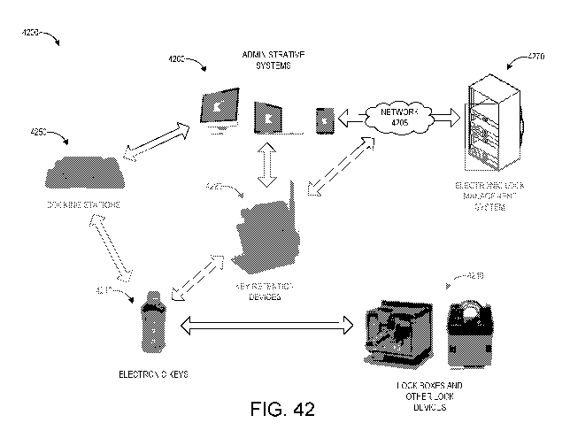
[0054] FIGURE 42 illustrates an example heuristic lock state detection
process.
[0055] FIGURES 43A and 43B illustrate example heuristic lock state
detection
processes.
[0056] FIGURE 44 depicts an example key retention device.
[0057] FIGURE 45 depicts an example audit trail user interface.
SUMMARY
[0058] The systems, methods and devices of this disclosure each have
several
innovative aspects, no single one of which is solely responsible for the all
of the desirable
attributes disclosed herein. Details of one or more implementations of the
subject matter
described in this specification are set forth in the accompanying drawings and
the description
below.
[0059] Certain aspects of the present disclosure relate to a method
for detecting a
lock state of an electronic lock. The method may be performed by an electronic
key or a
-5-
CA 03113243 2021-03-17
WO 2020/061221 PCT/US2019/051775
processor included with the electronic key. The electronic key may include: a
housing; a
power source disposed within the housing; a partial capacitor comprising a
first capacitive
metal plate, the first capacitive metal plate of the partial capacitor
configured to form a
capacitor with a corresponding second capacitive metal plate of an electronic
lock when
brought into proximity with the second capacitive metal plate of the
electronic lock; and a
processor in communication with the power source and with the partial
capacitor, the
processor programmed to transfer data signals to an electronic lock through
the first
capacitive metal plate to the second capacitive metal plate in the electronic
lock. The method
may include: mating the electronic key with the electronic lock; transmitting
an unlock signal
from the electronic key to the electronic lock; receiving, at the electronic
key, a confirmation
signal from the electronic lock, the confirmation signal indicating that the
electronic lock has
unlocked; recording, in a memory device of the electronic key, a first time at
which the
electronic lock has unlocked; transmitting a first heartbeat signal from the
electronic key to
the electronic lock; receiving, at the electronic key, a first response to the
first heartbeat
signal from the electronic lock; determining, by virtue of receiving the first
response, that the
electronic lock is still unlocked; transmitting one or more second heartbeat
signals from the
electronic key to the electronic lock; determining, after not receiving a
second response to the
one or more second heartbeat signals, that the electronic lock has relocked;
recording, in a
memory device of the electronic key, a second time at which the electronic
lock has relocked;
and outputting from the electronic key the first time at which the electronic
key has unlocked
and the second time at which the electronic key has relocked.
[0060] In some aspects, said determining, after not receiving a second
response to
the one or more second heartbeat signals, that the electronic lock has
relocked comprises
determining that the electronic lock has relocked after detecting no response
to three of the
second heartbeat signals, or some other defined number of second heartbeat
signals (e.g., 2, 4,
5, 10, or more, or some number in between the preceding examples). Further, in
some
aspects, said outputting is performed in response to docking the electronic
key with a docking
device. Moreover, said outputting may comprise transmitting the first time at
which the
electronic key has unlocked and the second time at which the electronic key
has relocked
over a network to a remote server. In some aspects, the electronic lock is
mated with the
-6-
CA 03113243 2021-03-17
WO 2020/061221 PCT/US2019/051775
electronic key in a manner such that when the electronic lock is unlocked and
the electronic
key is rotated to an open position, the electronic key is unable to be removed
from the
electronic lock while the electronic key remains in the open position.
[0061] Certain aspects of the present disclosure relate to a method
for detecting a
lock state of an electronic lock. The method may include transmitting an
unlock signal from
an electronic key to an electronic lock mated with the electronic key;
receiving, at the
electronic key, an confirmation signal from the electronic lock, the
confirmation signal
indicating that the electronic lock has unlocked; recording, in a memory
device of the
electronic key, a first time at which the electronic lock has unlocked;
transmitting a first
heartbeat signal from the electronic key to the electronic lock; receiving, at
the electronic key,
a first response to the first heartbeat signal from the electronic lock;
determining, by virtue of
receiving the first response, that the electronic lock is still unlocked;
transmitting one or more
second heartbeat signals from the electronic key to the electronic lock;
determining, after not
receiving a second response to the one or more second heartbeat signals, that
the electronic
lock has relocked; recording, in a memory device of the electronic key, a
second time at
which the electronic lock has relocked; and outputting from the electronic key
the first time at
which the electronic key has unlocked and the second time at which the
electronic key has
relocked.
[0062] In some aspects, said determining, after not receiving a second
response to
the one or more second heartbeat signals, that the electronic lock has
relocked comprises
determining that the electronic lock has relocked after detecting no response
to three
heartbeat signals. Further, said outputting may be performed in response to
docking the
electronic key with a docking device. In some cases, said outputting comprises
transmitting
the first time at which the electronic key has unlocked and the second time at
which the
electronic key has relocked over a network to a remote server. In addition,
the electronic lock
may be mated with the electronic key in a manner such that when the electronic
lock is
unlocked and the electronic key is rotated to an open position, the electronic
key is unable to
be removed from the electronic lock while the electronic key remains in the
open position.
[0063] Certain aspects of the present disclosure relate to a method of
detecting a
lock state of an electronic lock. The method may include: transmitting an
unlock signal from
-7-
CA 03113243 2021-03-17
WO 2020/061221 PCT/US2019/051775
an electronic key to an electronic lock; receiving, at the electronic key, a
confirmation signal
from the electronic lock, the confirmation signal indicating that the
electronic lock has
unlocked; recording, in a memory device of the electronic key, a first time at
which the
electronic lock has unlocked; transmitting one or more heartbeat signals from
the electronic
key to the electronic lock; determining, after not receiving a response to the
one or more
heartbeat signals, that the electronic lock has relocked; recording, in a
memory device of the
electronic key, a second time at which the electronic lock has relocked; and
outputting from
the electronic key the first time at which the electronic key has unlocked and
the second time
at which the electronic key has relocked.
[0064] In some cases, the unlock signal is transmitted after mating
the electronic
key with the electronic lock. Further, the unlock signal may be transmitted
after receiving or
confirming receipt of a keycode that matches a keycode stored at the
electronic lock.
Moreover, the one or more heartbeat signals may include a plurality of
heartbeat signals.
Further, the method may include receiving, at the electronic key, a first
response to a first
heartbeat signal included in the plurality of heartbeat signals from the
electronic lock; and
determining, by virtue of receiving the first response, that the electronic
lock is still unlocked.
The method may further include transmitting one or more additional heartbeat
signals
included in the plurality of heartbeat signals from the electronic key to the
electronic lock;
and determining, after not receiving a second response to the one or more
additional heartbeat
signals, that the electronic lock has relocked. Additionally, the method may
include
recording, in a memory device of the electronic key, a second time at which
the electronic
lock has relocked; and outputting from the electronic key the first time at
which the electronic
key has unlocked and the second time at which the electronic key has relocked.
[0065] Certain aspects of the present disclosure relate to an
electronic key. The
electronic key may include: a housing; a power source disposed within the
housing; a partial
capacitor comprising a first capacitive metal plate, the first capacitive
metal plate of the
partial capacitor configured to form a capacitor with a corresponding second
capacitive metal
plate of an electronic lock when brought into proximity with the second
capacitive metal
plate of the electronic lock; and a processor in communication with the power
source and
with the partial capacitor, the processor programmed to: transmit an unlock
signal from the
-8-
CA 03113243 2021-03-17
WO 2020/061221 PCT/US2019/051775
electronic key to the electronic lock when the electronic key is mated to the
electronic lock;
receive, at the electronic key, an confirmation signal from the electronic
lock, the
confirmation signal indicating that the electronic lock has unlocked; record,
in a memory
device of the electronic key, a first time at which the electronic lock has
unlocked; transmit a
first heartbeat signal from the electronic key to the electronic lock;
receive, at the electronic
key, a first response to the first heartbeat signal from the electronic lock;
determine, by virtue
of receiving the first response, that the electronic lock is still unlocked;
transmit one or more
second heartbeat signals from the electronic key to the electronic lock;
determine, after not
receiving a second response to the one or more second heartbeat signals, that
the electronic
lock has relocked; record, in a memory device of the electronic key, a second
time at which
the electronic lock has relocked; and output from the electronic key the first
time at which the
electronic key has unlocked and the second time at which the electronic key
has relocked.
[0066] In some implementations, the first capacitive metal plate
comprises an
annulus. Further, the electronic key may include: a key power coil, wherein
the key power
coil and the first capacitive metal plate are concentric; and a nose portion
disposed within a
hole formed by the annulus, wherein the key power coil is disposed at least
partially within
the nose portion. In some cases, the processor is programmed to determine,
after not
receiving a second response to the one or more second heartbeat signals, that
the electronic
lock has relocked by at least determining that the electronic lock has
relocked after detecting
no response to three of the second heartbeat signals. In certain aspects, the
electronic lock is
mated with the electronic key in a manner such that when the electronic lock
is unlocked and
the electronic key is rotated to an open position, the electronic key is
unable to be removed
from the electronic lock while the electronic key remains in the open
position.
[0067] Further, the processor may be programmed to output from the
electronic
key the first time at which the electronic key has unlocked and the second
time at which the
electronic key has relocked in response to docking the electronic key with a
docking device
or a docking station. In some cases, the docking station is configured to
secure the electronic
key in the docking device until a passcode is entered into the docking device.
In some cases,
the passcode is entered into the electronic key. In some such cases, the
electronic key may
provide the passcode to the docking device, which may determine whether to
unlock the
-9-
CA 03113243 2021-03-17
WO 2020/061221 PCT/US2019/051775
electronic key enabling removal of the electronic key from the docking device
based on
whether the passcode matches information stored at the docking device. In some
cases, the
docking device is configured to transmit the output from the electronic key to
a remote
server. Further, the output from the electronic key may constitute or comprise
audit trail data
that is stored in a cloud computing platform comprising the remote server.
Moreover, in
some implementations, the docking device is configured to charge the
electronic key.
DETAILED DESCRIPTION
[0068] In the description below certain relative terms such as top,
bottom, left,
right, front and back are used to describe the relationship between certain
components or
features of the illustrated embodiments. Such relative terms are provided as a
matter of
convenience in describing the illustrated embodiments and are not intended to
limit the scope
of the technology discussed below.
[0069] Electronic key and lock assemblies can advantageously
incorporate
contactless power and/or data transfer as a technique of electrical
communication between
key and lock components. In addition to inductive power and/or data transfer
using
transmitters and receivers fitted with electrical coils, an alternative
approach utilizes a
capacitive, rather than inductive, interface as a mechanism of delivering an
electrical signal.
Use of a capacitive interface may provide certain advantages over an inductive
interface. For
example, with a capacitor, electromagnetic fields may be generally confined
between and
around conductive plates of the capacitor, which can facilitate eliminating
magnetic flux
guiding and/or shielding components, thereby reducing bulk and/or cost
concerns.
[0070] Thus, in certain embodiments, an electronic key may include a
partial
capacitor comprising a capacitive metal plate in communication with a
processor. The
capacitive metal plate of the partial capacitor can form a capacitor with a
corresponding
capacitive metal plate of a lock when brought into proximity with the metal
plate of the lock,
thereby allowing for capacitive data or power transfer between the key and
lock. A common
ground can be established between the metal plate of the key and the metal
plate of the lock
through a parasitic capacitance present between the key and lock circuitry.
Prior to
describing such features, Figures 1-21 and the accompanying text below provide
an overview
-10-
CA 03113243 2021-03-17
WO 2020/061221 PCT/US2019/051775
of key and lock systems, some of which may incorporate capacitive data
transfer
characteristics.
I. Overview of the Key and Lock System
[0071] FIGURES 1 and 2 illustrate one embodiment of an electronic lock
and
key system, which is generally referred to by the reference numeral 10. The
electronic lock
and key system 10 includes a lock 100 and a key 200, which can engage one
another and to
selectively move the key 200 between a locked position and an unlocked
position. The lock
and key system 10 may be used to permit access to a location or enclosure in a
variety of
applications, such as a cabinet or other such storage compartment, for
example, which may
store valuable contents. Certain features, aspects and advantages of the lock
and key system
may be applied to other types of lock applications, such as selectively
permitting access to
buildings or automobiles, for example, or for selectively permitting operation
of a device.
Thus, although the present lock and key system 10 is disclosed herein in the
context of a
cabinet or storage compartment application, the technology disclosed herein
may be used
with, or adapted for use with, other suitable lock applications, as well.
[0072] The illustrated electronic lock and key system 10 can use
electronic means
to verify the identity of the key and to actuate the internal mechanism of the
lock 100. When
the key 200 engages the lock 100, data transfer and power transfer is enabled
between the
lock 100 and the key 200. The lock 100 is then preferably permitted to be
actuated by the key
200 to move from a locked position to an unlocked position and permit access
to the space or
location secured by the lock 100. In the illustrated arrangement, the
direction of power
transfer preferably is from the key 200 to the lock 100, as is described in
greater detail below.
However, in alternative arrangements, the direction of power transfer may be
reversed or may
occur in both directions.
[0073] The illustrated lock 100 is preferably used in a cabinet, or
other such
storage compartment, and can selectively secure a drawer or door of the
cabinet relative to a
body of the cabinet. However, as will be appreciated, the lock 100 may be used
in, or
adapted for use in, a variety of other applications. The lock 100 is
preferably mounted to the
cabinet in such a way so as to allow only a front portion of the lock 100 to
be accessible when
-11-
CA 03113243 2021-03-17
WO 2020/061221 PCT/US2019/051775
the cabinet is closed. The lock 100 includes an outer housing 102 with a
cylinder 104 that is
rotatable within the outer housing 102 when actuated by the key 200. An
exposed end of the
cylinder 104 can support a lock tab (not shown). The lock tab can cooperate
with a stop. The
lock 100 is associated with one of the drawer (or door) of the cabinet and the
cabinet body,
and the stop is associated with the other of the drawer (or door) of the
cabinet and the cabinet
body. The lock tab rotates with the lock cylinder 104 to move between a locked
position,
wherein the lock tab mechanically interferes with the stop, to an unlocked
position, wherein
the lock tab does not interfere with the stop. In addition, other suitable
locking arrangements
may be utilized.
II. Mechanical Aspects of the Key and Lock System
[0074] FIGURES 3 and 4 illustrate a cross-sectional view of the lock
100 of the
electronic lock and key assembly 10 of FIGURES 1 and 2. With additional
reference to the
FIGURES 3 and 4, the portion of the lock 100 on the left hand side of the
FIGURES will be
referred to as the front of the lock and the portion on the right hand side of
the FIGURES will
be referred to as the rear or back of the lock 100. As described above, the
lock 100 includes
the housing 102 and the cylinder 104. The cylinder 104 can be rotatable within
the housing
102 by the key 200 when the lock 100 and the key 200 are properly engaged. The
lock 100
further includes a cartridge 106, which includes a mechanism that can
selectively permit the
cylinder 104 to rotate within the housing 102. The lock 100 further includes a
mating portion
108 which can mate with the key 200 and an attack guard portion 110 which can
protect the
lock from unwanted tampering.
[0075] The housing 102 of the lock 100 preferably is a generally
cylindrical tube
with a head portion 112 and a body portion 114. The diameter of the head
portion 112 is
larger than the diameter of the body portion 114 such that the head portion
112 forms a flange
of the housing 102. The head portion 112 also includes an annular groove 174
or key recess.
Axially-extending slots 176 open into the annular groove 174 (FIGURE 2). The
groove 174
and slots 176 are used in engaging the key 200 with the lock 100 and are
described in greater
detail below. The head portion 112 can house a seal member, such as an 0-ring
116, which
-12-
CA 03113243 2021-03-17
WO 2020/061221 PCT/US2019/051775
is positioned to create a seal between the housing 102 and the cylinder 104.
Thus, the lock
100 is suitable for use in wet environments.
[0076] The lock housing 102 also includes a body portion 114 which
extends
rearwardly away from the head portion 112. The rearward end of the body
portion further
includes a threaded outer surface 115 which can receive a nut (not shown). The
nut is used to
secure the lock 100 to a cabinet or other storage compartment. The body
portion 114 also
includes at least one, and preferably a pair of opposed flattened surfaces 113
or "flats"
(FIGURE 2, only one shown), which are provided to reduce the likelihood of
rotation of the
housing 102 in a storage container wall or door. Alternatively, other
mechanisms may be
used to inhibit rotation of the housing 102 other than the flattened surfaces
113.
[0077] With continued reference to FIGURES 3 and 4, the body portion
114
further includes an internal groove 120 can secure the lock cylinder 104 from
rotation relative
to the lock housing 112 when the lock 100 is in a locked position. The groove
120 preferably
is open towards an interior passage 121 of the body portion 114, which houses
a portion of
the lock cylinder 104. The groove 120 extends axially along the body portion
114 and is
formed partially through a thickness of the body portion 114 in a radial
direction.
[0078] The body portion 114 further includes a tab 122 that extends
slightly
rearward from the rearward end of the body portion 114. The tab 122 acts as a
stop to limit
the rotation of a lock tab (not shown) secured to the cylinder 104.
[0079] The housing 102 can include a break-away feature incorporated
into the
structure of the housing 102. The head portion 112 is formed with the body
portion 114 in
such a way that if someone attempted to twist the housing 102 of the lock 100
by grasping the
head portion 112, the head portion 112 is capable of breaking free of the body
portion 114,
preferably at a location near the intersection of the head portion 112 and the
body portion 114
of the housing 102. This feature is advantageous in that it increases the
difficulty of opening
or disabling the lock 100 by grasping the housing 102. That is, if a person
were to attempt to
grasp the head portion 112 and it were to break away then there would no
longer be an easily
graspable surface with which to try to rotate the lock 100 mechanically,
without use of the
key 200, because the head portion 112, which is external to the cabinet, would
no longer be
coupled to the body portion 114, which is internal to the cabinet. The break-
away feature
-13-
CA 03113243 2021-03-17
WO 2020/061221 PCT/US2019/051775
between the head portion 112 and the body portion 114 may be created simply by
a structure
that concentrates stresses at the head portion 112/body portion 114 junction.
Alternatively,
the housing 102 may be deliberately weakened at or near the head portion
112/body portion
114 junction, or at any other desirably or suitable location. Other anti-
tampering solutions
may be employed as well.
[0080] With continued reference to FIGURES 3 and 4, as described
above, the
lock cylinder 104 includes a portion referred to as the cartridge 106. The
cartridge 106
includes a solenoid 126 with two adjacent slide bars 128. The slide bars 128
are spaced on
opposing sides of the solenoid 126 and can magnetically attract to the
solenoid 126 when the
lock 100 is in the locked position. The slide bars 128 preferably are
constructed with a
neodymium-containing material, which may be encapsulated in a stainless steel
material for
corrosion protection and wear resistance. When the lock 100 is moved to an
unlocked
position, the solenoid 126 can reverse polarity such that the slide bars 128
are magnetically
repelled from the solenoid 126, as is described in greater detail below.
Preferably, the slide
bars 128 are movable along an axis that is parallel to (which includes coaxial
with) a
longitudinal axis of the lock 100.
[0081] The cartridge 106 is surrounded by a tamper-resistant case 124
that houses
a circuit board 134 can receive instructions when the key 200 engages with the
lock 100. The
circuit board 134 is can recognize the proper protocol used to unlock the lock
100. The
circuit board 134 is further can actuate the solenoid 126 to reverse the
polarity of the solenoid
126 and repel the slide bars 128 away from the solenoid 126. The details of
the circuit board
134 and a method of communication between the key 200 and the lock 100 are
discussed in
greater detail below. The interior of the case 124 preferably is filled with a
filler material,
such as an epoxy, to occupy empty space within the case 124 and protect and
maintain a
desired position of the components within the case 124, such as the circuit
board 134 and
wires 160.
[0082] The lock cartridge 106 further includes two slide tubes 136
which are
positioned on opposite sides of the solenoid 126 and are can at least
partially encapsulate the
slide bars 128 and are further can provide a smooth, sliding surface for the
slide bars 128.
-14-
CA 03113243 2021-03-17
WO 2020/061221 PCT/US2019/051775
The slide tubes 136 each include an aperture 138 can receive at least a
portion of a bolt 130,
or side bar, of the lock 100 when the lock 100 is in an unlocked position.
[0083] The bolt 130 is preferably a relatively thin, generally block-
shaped
structure that is movable between a locked position, in which rotation of the
lock cylinder
104 relative to the housing 102 is prohibited, and an unlocked position, in
which rotation of
the lock cylinder 104 relative to the housing 102 is permitted. Preferably,
the bolt 130 moves
in a radial direction between the locked position and the unlocked position,
with the unlocked
position being radially inward of the locked position.
[0084] The bolt 130 includes two cylindrical extensions 131, which
extend
radially inward toward the cartridge 106. When the solenoid 126 is actuated to
repel the slide
bars 128 such that the apertures 138 are not blocked by the slide bars 128,
the extensions 131
of the bolt 130 may enter into the case 124 through the apertures 138 as the
bolt 130 moves
radially inward.
[0085] The bolt 130 is preferably of sufficient strength to
rotationally secure the
cylinder 104 relative to the housing 102 when the bolt 130 is in the locked
position, wherein
a portion of the bolt 130 is present within the groove 120. The bolt 130 has a
sloped or
chamfered lower edge 129, which in the illustrated embodiment is substantially
V-shaped.
The lower edge 129 can mate with the groove 120, which preferably is of an at
least
substantially correspondingly shape to the lower edge 129 of the bolt 130. The
V-shaped
edge 129 of the bolt 130 interacting with the V-shaped groove 120 of the
housing 102 urges
the bolt 130 in a radially inward direction towards the cartridge 106 in
response to rotation of
the cylinder 104 relative to the housing 102. That is, the sloped lower edge
129 and groove
120 cooperate to function as a wedge and eliminate the need for a mechanism to
positively
retract the bolt 130 from the groove 120. Such an arrangement is used in
certain
embodiments due to its simplicity and reduction in the number of necessary
parts. However,
other suitable arrangements to lock and unlock the cylinder 104 relative to
the housing 102
may also be used.
[0086] When the lock 100 is in an unlocked condition and the slide
bars 128 are
spaced from the solenoid 126, as shown in FIGURE 4, the bolt 130 is free to
move radially
inward (or upward in the orientation of FIGURE 4) into the cartridge 106, thus
allowing the
-15-
CA 03113243 2021-03-17
WO 2020/061221 PCT/US2019/051775
cylinder 104 to rotate within the housing 102. Preferably, one or more biasing
members,
such as springs, tend to urge the bolt 130 toward a locked position. In the
illustrated
arrangement, two springs 132 are provided to produce such a biasing force on
the bolt 130.
[0087] When the lock 100 is in a locked condition, the bolt 130 is
extended
radially outward into engagement with the groove 120. The bolt 130 is
prevented from
inward movement out of engagement with the groove 120 due to interference
between the
extensions 131 and the slide bars 128. When the lock 100 is in the unlocked
position, the
slide bars 128 are moved away from the solenoid 126 due to a switching of
magnetic polarity
of the solenoid 126, which is actuated by the circuit board 134. The bolt 130
is then free to
move radially inward towards the center of the cylinder 104 and out of
engagement with the
groove 120. At this point, the rotation of the cylinder 104 within the housing
102 may cause
the bolt 130 to be displaced from engagement with the groove 120 due to the
cooperating
sloped surfaces of the groove 120 and the lower edge 129 of the bolt 130. The
cylinder 104
is then free to be rotated throughout the unlocked rotational range within the
housing 102.
When the cylinder 104 is rotated back to a locked position, that is, when the
lower edge 129
of the bolt 130 is aligned with the groove 120, the bolt 130 is urged radially
outward by the
springs 132 such that the lower edge 129 is engaged with the groove 120. Once
the
extensions 131 of the bolt 130 are retracted from the case 124 to a sufficient
extent, the slide
bars 128 are able to move towards the solenoid 126 to once again establish the
locked
position of the lock 100.
[0088] Although FIGURE 3 and FIGURE 4 show a housing 102 with only one
groove 120, multiple grooves 120 may be provided within the housing 102 in
other
embodiments. Such a configuration may be advantageous in that multiple bolts
130 may be
provided, or if it is desirable to have multiple locked positions using a
single bolt 130
interacting with one of several available grooves 120.
[0089] With continued reference to FIGURES 3 and 4, the lock 100
further
includes an attack guard portion 110 can inhibit access to the cartridge 106
such as by
drilling, for example, from the exposed portions of the lock, such as the head
portion 112.
The illustrated attack guard portion 110 includes a radial array of pins 140
and an attack ball
142, which are located along the longitudinal axis of the lock 100 between the
mating portion
-16-
CA 03113243 2021-03-17
WO 2020/061221 PCT/US2019/051775
108 and the cartridge 106. In the illustrated arrangement, the attack ball 142
is generally
centered relative to the longitudinal axis of the lock 100 and is surrounded
by the pins 140.
[0090] The pins 140 are preferably made from a carbide material, but
can be made
of any suitable material or combination of materials that are capable of
providing a suitable
hardness to reduce the likelihood of successful drilling past the pins 140 and
attack ball 142.
The pins 140 are inserted into the cylinder 104 to a depth that is near the
outer extremity of
the attack ball 142. A small space may be provided between the outer end of
the attack ball
142 and the end of the carbide pin 140 to allow for the passage of the wires
160, which is
discussed in greater detail below. The pins 140 are provided so as to add
strength and
hardness to the outer periphery of the cylinder 104 adjacent to the attack
ball 142.
[0091] The attack ball 142 is preferably made of a ceramic material
but, similar to
the carbide pins, can be made of any suitable material that is of sufficient
hardness to reduce
the likelihood of successful drilling of the lock cylinder 104. The attack
ball 142 is
preferably generally spherical shape and lies within a pocket on substantially
the same axis as
the cartridge 106. Preferably, the attack ball 142 is located in front of the
cartridge 106 and is
aligned along the longitudinal axis of the lock 100 with the pins 140. The
attack ball 142 can
reduce the likelihood of a drill bit passing through the cylinder and drilling
out the cartridge
106. It is preferable that if an attempt is made to drill out the cylinder
104, the attack ball 142
is sufficiently hard as to not allow the drill bit to drill past the ball 142
and into the cartridge
106. The shape of the attack ball 142 is also advantageous in that it will
likely deflect a drill
bit from drilling into the cartridge 104 by not allowing the tip of the drill
bit to locate
centrally relative to the lock 100. Because the attack ball 142 is held within
a pocket, it
advantageously retains functionality even if cracked or broken. Thus, the
attack guard
portion 110 can substantially reduce the likelihood of success of an attempt
to drill out the
cartridge 106. In addition, or in the alternative, other suitable arrangements
to prevent
drilling, or other destructive tampering, of the lock 100 may be used as well.
[0092] One advantage of using the pins 140 and the attack ball 142 is
that the
entire lock cylinder 104 does not have to be made of a hard material. Because
the lock
cylinder 104 includes many features that are formed in the material by shaping
(e.g., casting
or forging) or material removal (e.g., machining), it would be very difficult
to manufacture a
-17-
CA 03113243 2021-03-17
WO 2020/061221 PCT/US2019/051775
cylinder 104 entirely of a hard material such as ceramic or carbide. By using
separate pins
140 and an attack ball 142, which are made of a very hard material that is
difficult to drill, the
lock cylinder 104 can be easily manufactured of a material such as stainless
steel which has
properties that allow easier manufacture. Thus a lock cylinder can be made
that is both
relatively easy to manufacture, but also includes drill resistant properties.
[0093] With continued reference to FIGURES 3 and 4, the lock 100
includes a
mating portion 108 located near the front portion of the lock 100. The mating
portion 108
preferably includes a mechanical mating portion 144 and a data and power
mating portion
146. The mechanical mating portion 144 includes a tapered cylindrical
extension 148 that
extends in a forward direction from the lock cylinder 104 and can be received
within a
portion of the key 200 when the lock 100 and the key 200 are engaged together.
At the base
of the extension 148 are two recesses 150 that can mate with two extensions,
or protrusions,
on the key 200, which are described in greater detail below. The recesses 150
can allow the
key 200 to positively engage the cylinder 104 such that torque can be
transferred from the key
200 to the cylinder 104 upon rotation of the key 200.
[0094] The data and power mating portion 146 includes a mating cup
152, a data
coil 154, and a power coil 156. The cup 152 can receive a portion of key 200
when the lock
100 and the key 200 are engaged together. The cup 152 resides at least
partially in an axial
recess 158 which is located in a front portion of the lock cylinder 104 and
further houses the
attack ball 142. The cup is at least partially surrounded by the power coil
156, which can
inductively receive power from the key 200. The cup 152 preferably includes
axial slots 161
that can allow power to transmit through the cup 152.
[0095] The data coil 154 is located towards the upper edge of the cup
152 and,
preferably, lies just rearward of the forward lip of the cup 152. The data
coil 154 is generally
of a torus shape and can cooperate with a data coil of the key 200, as is
described in greater
detail below. Two wires 160 extend from the cup 152, through a passage 162,
and into the
lock cartridge 106. The wires 160 preferably transmit data and power from the
data and
power mating portion 146 to the solenoid 126 and the circuit board 134.
[0096] The power coil 156 is preferably aligned with a longitudinal
axis of the
lock 100 so that a longitudinal axis passing through the power coil 156 is
substantially
-18-
CA 03113243 2021-03-17
WO 2020/061221 PCT/US2019/051775
parallel (or coaxial) with a longitudinal axis of the lock 100. The data coil
154 is preferably
arranged to generally lie in a plane that is orthogonal to a longitudinal axis
of the lock. Such
an arrangement helps to reduce magnetic interference between the transmission
of power
between the lock 100 and the key 200 and the transmission of data between the
lock 100 and
the key 200.
[0097] As described above, the lock cylinder 104 can support a lock
tab, which
interacts with a stop to inhibit opening of a cabinet drawer or door, or
prevent relative
movement of other structures that are secured by the lock and key system 10.
The lock
cylinder 104 includes a lock tab portion 164 that can support a lock tab in a
rotationally fixed
manner relative to the lock cylinder 104. The lock tab portion 164 includes a
flatted portion
166 and a threaded portion 168. The flatted portion 166 can receive a lock tab
(not shown)
which can slide over lock tab portion 164 and mate with the flatted portion
166. One or more
flat surfaces, or "flats," on the flatted portion 166 can allow the
transmission of torque from
the cylinder 104 to the lock tab (not shown). The threaded portion 168 can
receive a nut (not
shown), which can secure the lock tab (not shown) to the cylinder 104.
[0098] FIGURES 5-7 illustrate an embodiment of the key 200 that may be
used
with the lock 100 of the electronic lock and key assembly 10. The key 200 can
mate with the
lock 100 to permit power and data communication between the key 200 and the
lock 100. In
the illustrated arrangement, the key 200 can also mechanically engage the lock
100 to move
the lock from a locked to an unlocked position or vise versa.
[0099] The key 200 includes an elongate main body section 204 that is
generally
rectangular in cross-sectional shape. The key 200 also includes a nose section
202 of smaller
external dimensions than the body section 204. An end section 206 closes and
end portion of
the body section 204 opposite the nose section 202. The nose section 202 can
engage the
lock 100 and the body section 204 can house the internal electronics of the
key 200 as well as
other desirable components. The end section 206 is removable from the body
section 204 to
permit access to the interior of the body section 204.
[0100] With continued reference to FIGURES 5-7, the nose section 202
includes
a tapered transition portion 208 which extends between a cylindrical portion
210 of the nose
-19-
CA 03113243 2021-03-17
WO 2020/061221 PCT/US2019/051775
section 202 and the body section 204. The cylindrical portion 210 houses the
power and data
transfer portion 212 of the key 200, which is discussed in greater detail
below.
[0101] On the outer surface of the cylindrical portion are two
radiused tabs 214
which can rotationally locate the key 200 relative to the lock 100 prior to
the key 200
engaging the lock 100. The tabs 214 extend radially outward from the outer
surface of the
cylindrical portion 210 and, preferably, oppose one another.
[0102] The cylindrical portion 210 further includes two generally
rectangular
extensions 216 that extend axially outward and can engage with the recesses
150 of the lock
100 (FIGURE 3) when the key 200 engages the lock 100. The rectangular
extensions 216
can couple the nose section 202 of the key 200 to the lock cylinder 104 and to
transmit torque
from the key 200 to the cylinder 104 when the key 200 is rotated.
[0103] The cylindrical portion 210 includes a recess 218 that opens to
the front of
the key 200. Located within the recess 218 is the power and data transfer
portion 212 of the
key 200. Preferably, the power and data transfer portion 212 is generally
centrally located
within the recess 218 and aligned with the longitudinal axis of the key 200.
The power and
data transfer portion 212 includes a power coil 220 and a data coil 222. The
power coil 220
is generally cylindrical in shape with a slight taper along its axis. The
power coil 220 is
positioned forward of the data coil 222 and, preferably, remains within the
recess 218 of the
cylindrical portion 210. The power coil 220 can be inductively coupled with
the power coil
152 of the lock 100. The data coil 222 is generally toroidal in shape and is
located at the base
of the recess 218. The data coil 222 can be inductively coupled with the data
coil 154 of the
lock 100, as is described in greater detail below.
[0104] With continued reference to FIGURES 5-7, in the illustrated
arrangement,
the nose section 202 is a separate component from the body section 204 and is
connected to a
forward end of the body section 204 of the key 200. The nose section 202 mates
with the
body section 204 and is sealed by a suitable seal member, such as 0-ring 224,
which inhibits
contaminants from entering the interior of the key 200. The nose section 202
is secured to
the body section by two fastening members, such as screws 226 (FIGURES 1 and
5).
Similarly, the end section 206 is a separate component from the body section
204 and is
coupled to a rearward end of the body section 200. The end section is
substantially sealed to
-20-
CA 03113243 2021-03-17
WO 2020/061221 PCT/US2019/051775
the body section 204 by a suitable seal member, such as 0-ring 230, which can
inhibit
contaminants from entering the interior of the key 200. Thus, the key 200
preferably is
suitable for use in wet environments. The end section 206 is secured to the
body section 204
by a fastening member, such as screw 232, which can retain the end section 206
to the body
section 204.
[0105] The body section 204 includes three externally-accessible input
buttons
228 extending from the body section 204 (upward in the orientation of FIGURE
5). The
input buttons 228 are in electrical contact with a processing unit 229 of the
key 200, which
preferably includes a processor and a memory. The input buttons 228 permit
data to be
entered into the key 200, such as a wake-up or programming code, for example.
Certain
functional features of the key 200 are described in greater detail below with
reference to
FIGURES 9-12.
[0106] With reference to FIGURES 6 and 7, the key 200 further includes
a
plurality of axially-extending cavities 236. The illustrated key 200 includes
four cavities 236.
The axial cavities 236 extend through at least a significant portion of the
length of the body
section 204 and are preferably circular in cross-sectional shape. The axial
cavities 236 can
house battery cells (not shown) that provide a source of power within the key
200, which
provides power to the lock 100 when the key 200 and the lock 100 are engaged.
The cavities
236 are preferably arranged in a side-by-side manner and surround a
longitudinal axis of the
key 200. The key 200 preferably includes a power source (discussed below) and
can be
rechargeable. Preferably, the key 200 includes a recharge port (not shown),
which can mate
with an associated recharge port of a recharger (not shown) when it is desired
to recharge the
key 200.
[0107] With reference to FIGURES 2 and 8, the key 200 is shown about
to
engage the lock 100, and engaging the lock 100, respectively. When the key 200
engages
with the lock 100, desirably, certain mechanical operations occur and certain
electrical
operations occur. When engaging the key 200 with the lock 100, the key 200 is
rotationally
positioned relative to the lock 100 such that the tabs 214 of the key 200 are
aligned with the
slots 176 (FIGURE 2) of the lock 100. The key 200 is then displaced axially
such that the
tabs 214 pass through the slots 176 and the cylindrical portion 210 of the key
200 is
-21-
CA 03113243 2021-03-17
WO 2020/061221 PCT/US2019/051775
positioned within the housing 102 of the lock 100. The key 200 is sized and
shaped such that
the tabs 214 are located within the annular groove 174, which has a shape that
closely
matches the profile of the tabs 214. In this relative position, the key 200 is
able to rotate
within the housing 100, so long as the key 200 is a proper match for the lock
100 and the lock
is moved to the unlocked position, as is described in greater detail below.
[0108] Furthermore, when the key 200 engages the lock 100, the
cylindrical
extension 148 of the lock 100 is received within the recess 218 of the key.
The recess 218 is
defined by a tapered surface which closely matches a tapered outer surface of
the cylindrical
extension 148. The cooperating tapered surfaces facilitate smooth engagement
of the lock
100 and key 200, while also ensuring proper alignment between the lock 100 and
key 200.
Furthermore, the rectangular extensions 216 of the key 200 insert into the
recesses 150 of the
lock 100 to positively engage the key 200 with the lock 100 so that rotation
of the key 200
results in rotation of the lock cylinder 104 within the housing 102.
[0109] When the key 200 engages the lock 100, the power coil 220 of
the key 200
is aligned for inductive coupling with the power coil 156 of the lock 100.
Also, the data coil
222 of the key 200 is aligned for inductive coupling with the data coil 154 of
the lock 100.
Preferably, the power coil 220 of the key 200 is inserted into the cup portion
152 of the lock
100 and thus the power coil 156 of the lock 100 and the power coil 220 of the
key 200 at least
partially overlap along the longitudinal axis of the lock 100 and/or key 200.
Furthermore,
preferably, the data coil 154 of the lock 100 and the data coil 222 of the key
200 come into
sufficient alignment for inductive coupling when the key 200 engages the lock
100. That is,
in the illustrated arrangement, when the key 200 engages the lock 100, the
data coil 222 of
the key 200 and the data coil 154 of the lock 100 are positioned adjacent one
another and,
desirably, are substantially coaxial with one another. Furthermore, a plane
which passes
through the data coil 222 of the key 200 preferably is substantially parallel
to a plane which
passes through the data coil 154 of the lock 100. Desirably, the spacing
between the data
coils 154 and 222 is within a range of about 30-40 mils (or 0.03-0.04 inches).
Such an
arrangement is beneficial to reduce interference between the power transfer
and the data
transfer between the lock 100 and key 200, as is described in greater detail
below. However,
in other arrangements, a greater or lesser amount of spacing may be desirable.
-22-
CA 03113243 2021-03-17
WO 2020/061221 PCT/US2019/051775
[0110] In the illustrated embodiment of the lock and key system 10,
when the key
200 engages the lock 100 there are two transfers that occur. The first
transfer is a transfer of
data and the second transfer is a transfer of power. During engagement of the
key 200 and
the lock 100, the data coils 222 and 154, in the illustrated embodiments, do
not come into
physical contact with one another. Similarly, the power coil 200 of the key
200 and power
coil 156 of the lock 100, in the illustrated embodiment, do not come into
physical contact
with one another. The data is preferably transferred between the data coil 222
of the key 200
and the data coil 154 of the lock 100 by induction, as described in connection
with FIGURE
9 below. The power is also transferred between the power coil 200 of the key
200 and the
power coil 156 of the lock 100 preferably once again by induction, as is also
described in
connection with FIGURE 9 below. When engagement between the key 200 and the
lock 100
has been made, a data protocol occurs which signals to the circuit board 134
that the proper
key 200 has been inserted into the lock 100. Power is transferred from the key
200 to the
lock 100 to activate the solenoid 126, which permits the lock 100 to be
unlocked by rotation
of the key 200.
III. Electrical Aspects of the Key and Lock System
[0111] FIGURE 9 depicts an embodiment of a magnetic field diagram 400.
In
the magnetic field diagram 400, a cross-section view of a power coil 402,
interior power coil
418, first data coil 406, and second data coil 408 are depicted in relation to
a power magnetic
field 404 and a data magnetic field 410 generated by the coils 406 and 408. In
the depicted
embodiment, the configuration of the power coil 402, interior power coil 418,
first data coil
406, and second data coil 408 causes the power magnetic field 404 to be
orthogonal or
substantially orthogonal to the data magnetic field 410 at certain locations.
This orthogonal
relationship facilitates data transfer between the data coils 406, 408 with
little or no
interference from the power magnetic field 404. The coils 402, 406, 408 and
418, as
illustrated, correspond with the power and data coils of the lock 100 and key
200 of
FIGURES 1-8. In particular, the power coil 402 corresponds with the lock power
coil 156,
the interior power coil 418 corresponds with the key power coil 220, the data
coil 406
corresponds with the lock data coil 154 and the data coil 408 corresponds with
the key data
-23-
CA 03113243 2021-03-17
WO 2020/061221 PCT/US2019/051775
coil 222. However, the physical relationships between the coils may be altered
in alternative
embodiments from the locations shown in FIGURES 1-8; however, preferably the
interference reduction or elimination concepts disclosed herein are still
employed.
[0112] The power coil 402 of certain embodiments is a solenoid. The
solenoid
includes windings 420 which are loops of wire that are wound tightly into a
cylindrical shape.
In the depicted embodiment, the power coil 402 includes two sets of windings
420. Two sets
of windings 420 in the power coil 402 reduce air gaps between the wires and
thereby increase
the strength of a magnetic field generated by the power coil 402.
[0113] The depicted embodiment of the power coil 402 does not include
a
magnetic core material, such as an iron core, although in certain embodiments,
a magnetic
core material may be included in the power coil 402. In other embodiments,
while the power
coil 402 is depicted as a solenoid, other forms of coils other than solenoids
may be used.
[0114] The power coil 402 may form a portion of a lock assembly,
though not
shown, such as any of the lock assemblies described above. Alternatively, the
power coil 402
may be connected to a key assembly, such as any of the key assemblies
described above. In
addition, the power coil 402 may be connected to a docking station (not
shown), as described
in connection with FIGURE 10, below.
[0115] The power coil 402 is shown having a width 414 (also denoted as
The width 414 of the power coil 402 is slightly flared for the entire length
of the power coil
402. The overall shape of the power coil 402, including its width 414,
determines in part the
shape of the magnetic field emanating from the power coil 402. In certain
embodiments, a
constant or approximately constant width 414 of the power coil 402 does not
change the
shape of the power magnetic field 404 substantially from the shape illustrated
in FIGURE 9.
[0116] The power coil 402 further includes a casing 462 surrounding
the power
coil 402. In one embodiment, the casing 462 is a non-conducting material
(dielectric). The
casing 462 of certain embodiments facilitates the power coil 402 receiving the
interior power
coil 418 inside the power coil 402. The casing 462 prevents electrical contact
between the
power coil 402 and the interior power coil 418. Thus, in the embodiment
described with
reference to FIGURES 1-8, the cup 152 of the lock 100 may be constructed from,
or include,
-24-
CA 03113243 2021-03-17
WO 2020/061221 PCT/US2019/051775
an insulation material. Furthermore, other physical structures interposed
between adjacent
coils may be made from, or include, insulating materials.
[0117] In alternative embodiments, the casing 462 is made of a metal,
such as
steel. The strength of a metal casing 462 such as steel helps prevent
tampering with the
power coil 402. However, magnetic fields often cannot penetrate more than a
few layers of
steel and other metals. Therefore, the metal casing 462 of certain embodiments
includes one
or more slits or other openings (not shown) to allow magnetic fields to pass
between the
power coil 402 and the interior power coil 418.
[0118] The interior power coil 418 mates with the power coil 402 by
fitting inside
the power coil 402. In certain embodiments, the interior power coil 418 has
similar
characteristics to the power coil 402. For instance, the interior power coil
418 in the depicted
embodiment is a solenoid with two windings 420. In addition, the interior
power coil 418
may receive a current and thereby generate a magnetic field. The interior
power coil 418 is
also covered in a casing material 454, which may be an insulator or metal
conductor, to
facilitate mating with the power coil 402. Furthermore, the interior power
coil 418 also has a
width 430 (also denoted "Wi") that is less than the width 414 of the power
coil 402, thereby
allowing the interior power coil 418 to mate with the power coil 402.
[0119] In addition to these features, the interior power coil 418 of
certain
embodiments includes a ferromagnetic core 452, which may be a steel, iron, or
other metallic
core. The ferromagnetic core 452 increases the strength of the power magnetic
field 404,
enabling a more efficient power transfer between the interior power coil 418
and the power
coil 402. In addition, the ferromagnetic core 452 in certain embodiments
enables the
frequency of the power signal to be reduced, allowing a processor in
communication with the
power coil 418 to operate at a lower frequency and thereby decrease the cost
of the processor.
[0120] The interior power coil 418 may form a portion of a lock
assembly, though
not shown, such as any of the lock assemblies described above. Alternatively,
the interior
power coil 418 may be connected to a key assembly, such as any of the key
assemblies
described above. In addition, the interior power coil 418 may be connected to
a docking
station (not shown), as described in connection with FIGURE 10, below.
-25-
CA 03113243 2021-03-17
WO 2020/061221 PCT/US2019/051775
[0121] A changing current flow through the interior power coil 418
induces a
changing magnetic field. This magnetic field, by changing with respect to
time, induces a
changing current flow through the power coil 402. The changing current flow
through the
power coil 402 further induces a magnetic field. These two magnetic fields
combine to form
the power magnetic field 404. In such a state, the power coil 402 and the
interior power coil
418 are "inductively coupled," which means that a transfer of energy from one
coil to the
other occurs through a shared magnetic field, e.g., the power magnetic field
402. Inductive
coupling may also occur by sending a changing current flow through the power
coil 402,
which induces a magnetic field that in turn induces current flow through the
interior power
coil 418. Consequently, inductive coupling may be initiated by either power
coil.
[0122] Inductive coupling allows the interior power coil 418 to
transfer power to
the power coil 402 (and vice versa). An alternating current (AC) signal
flowing through the
interior power coil 418 is communicated to the power coil 402 through the
power magnetic
field 404. The power magnetic field 404 generates an identical or
substantially identical AC
signal in the power coil 402. Consequently, power is transferred between the
interior power
coil 418 and the power coil 402, even though the coils are not in electrical
contact with one
another.
[0123] In certain embodiments, the interior power coil 418 has fewer
windings
than the power coil 402. A voltage signal in the interior power coil 418 is
therefore amplified
in the power coil 402, according to known physical relationships in the art.
Likewise, a
voltage signal in the power coil 402 is reduced or attenuated in the interior
power coil 418.
In addition, the power coil 402 may have fewer windings than the interior
power coil 418,
such that a voltage signal from the interior power coil 418 to the power coil
402 is attenuated,
and a voltage signal from the power coil 402 to the interior power coil 418 is
amplified.
[0124] The power magnetic field 404 is shown in the depicted
embodiment as
field lines 434; however, the depiction of the power magnetic field 404 with
field lines 434 is
a model or representation of actual magnetic fields, which in some embodiments
are
changing with respect to time. Therefore, the power magnetic field 404 in
certain
embodiments is depicted at a moment in time. Moreover, the depicted model of
the power
-26-
CA 03113243 2021-03-17
WO 2020/061221 PCT/US2019/051775
magnetic field 404 includes a small number of field lines 434 for clarity, but
in general the
power magnetic field 404 fills all or substantially all of the space depicted
in FIGURE 9.
[0125] Portions of the field lines 434 of the power magnetic field 404
on the
outside of the power coil 402 are parallel or substantially parallel to the
axis of the power coil
402. The parallel nature of these field lines 434 in certain embodiments
facilitates
minimizing interference between power and data transfer, as is described
below.
[0126] The first data coil 406 is connected to the power coil 402 by
the casing
462. The first data coil 406 has one or more windings 422. In one embodiment,
the first data
coil 406 is a toroid including tightly-wound windings 422 around a
ferromagnetic core 472,
such as steel or iron. The ferromagnetic core 472 of certain embodiments
increases the
strength of a magnetic field generated by the first data coil 406, thereby
allowing more
efficient transfer of data through the data magnetic field 410. In addition,
the ferromagnetic
core 472 in certain embodiments enables the frequency of the data signal to be
reduced,
allowing a processor in communication with the first data coil 406 to operate
at a lower
frequency and thereby decreasing the cost of the processor.
[0127] Though not shown, the first data coil 406 may further include
an insulation
material surrounding the first data coil 406. Such insulation material may be
a non-
conducting material (dielectric). In addition, the casing 462 covering the
power coil 402 in
certain embodiments also at least partially covers the first data coil 406, as
shown. The
casing 462 at the boundary between the first data coil 406 and the second data
coil 408 may
also include a slit or other opening to allow magnetic fields to pass between
the first and
second data coils 406, 408.
[0128] The first data coil 406 has a width 416 (also denoted as "Wd").
This width
416 is greater than the width 414 of the power coil 402 in some
implementations. In
alternative embodiments, the width 416 may be equal to or less than the width
414 of the
power coil 402.
[0129] The second data coil 408 in the depicted embodiment is
substantially
identical to the first data coil 406. In particular, the second data coil 408
is a toroid including
tightly-wound windings 424 around a ferromagnetic core 474, such as steel or
iron. The
ferromagnetic core 474 of certain embodiments increases the strength of a
magnetic field
-27-
CA 03113243 2021-03-17
WO 2020/061221 PCT/US2019/051775
generated by the second data coil 408, thereby allowing more efficient
transfer of data
through the data magnetic field 410, allowing a processor in communication
with the second
data coil 408 to operate at a lower frequency and thereby decreasing the cost
of the processor.
[0130] The
second data coil 408 in the depicted embodiment has a width 416
equal to the width 414 of the first data coil 406. In addition, the second
data coil 408 may
have an insulating layer (not shown) and may be covered by the casing 454, as
shown.
However, in certain embodiments, the second data coil 408 has different
characteristics from
the first data coil 406, such as a different number of windings 424 or a
different width 416.
In addition, first and second data coils 406, 408 having different widths may
overlap in
various ways.
[0131]
When a current is transmitted through either the first data coil 406 or the
second data coil 408, the first data coil 406 and the second data coil 408 are
inductively
coupled, in a similar manner to the inductive coupling of the power coil 402
and the interior
power coil 418. Data in the form of voltage or current signals may therefore
be
communicated between the first data coil 406 and the second data coil 408. In
certain
embodiments, data may be communicated in both directions. That is, either the
first or
second data coil 406, 408 may initiate communications. In
addition, during one
communication session, the first and second data coils 406, 408 may alternate
transmitting
data and receiving data.
[0132]
Data magnetic field 410 is depicted as including field lines 442, a portion
of which are orthogonal or substantially orthogonal to the data coils 406, 408
along their
width 416. Like the field lines 434, 436 of the power magnetic field 404, the
field lines 442
of the data magnetic field 410 are a model of actual magnetic fields that may
be changing in
time. The orthogonal nature of these field lines 442 in certain embodiments
facilitates
minimizing the interference between power and data transfer.
[0133] In
various embodiments, at least a portion of the data magnetic field 410 is
orthogonal to or substantially orthogonal to the power magnetic field 404 at
certain areas of
orthogonality. These areas of orthogonality include portions of an interface
412 between the
first data coil 406 and the second data coil 408. This interface 412 in
certain embodiments is
an annular or circumferential region between the first data coil 406 and
second data coil 408.
-28-
CA 03113243 2021-03-17
WO 2020/061221 PCT/US2019/051775
At this interface, at least a portion of the data magnetic field 410 is
substantially parallel to
the first data coil 406 and second data coil 408. Because the data magnetic
field 410 is
substantially parallel to the data coils 406, 408, the data magnetic field 410
is therefore
substantially orthogonal to the power magnetic field 404 at portions of the
interface 412.
[0134] According to known relationships in the physics of magnetic
fields,
magnetic fields which are orthogonal to each other have very little effect on
each other.
Thus, the power magnetic field 404 at the interface 412 has very little effect
on the data
magnetic field 410. Consequently, the data coils 406 and 408 can communicate
with each
other with minimal interference from the potentially strong power magnetic
field 404. In
addition, data transmitted between the data coils 406, 408 does not interfere
or minimally
interferes with the power magnetic field 404. Thus, data may be sent across
the data coils
406, 408 simultaneously while power is being sent between the power coil 402
and the
interior power coil 418.
[0135] FIGURE 10 depicts embodiments of a key circuit 510 and a lock
circuit
530. In the depicted embodiment, the key circuit 510 is shown in proximity to
the lock
circuit 530. The relative locations of the key circuit 510 and the lock
circuit 530 shows that
in certain implementations components of the key circuit 510 interface with
components of
the lock circuit 530. Moreover, the key circuit 510 may in certain embodiments
be contained
in a key assembly such as any of the keys described above. Likewise, the lock
circuit 530
may be contained in a lock assembly such as any of the locks described above.
[0136] The key circuit 510 includes a processor 502. The processor 502
may be a
microprocessor, a central processing unit (CPU), a microcontroller, or other
type of
processor. The processor 502 in certain embodiments implements program code.
By
implementing program code, the processor 502 sends certain signals to the lock
circuit 530
and receives signals from the lock circuit 530. Such signals may include power
signals, data
signals, and the like.
[0137] A memory device 526 is in communication with the processor 502.
The
memory device 526 in certain embodiments is a flash memory, hard disk storage,
an
EEPROM, or other form of storage. The memory device 526 in certain embodiments
stores
-29-
CA 03113243 2021-03-17
WO 2020/061221 PCT/US2019/051775
program code to be run on the processor 502. In addition, the memory device
526 may store
data received from the processor 502.
[0138] Data stored on the memory device 526 may include encryption
data. In
one embodiment, the encryption data includes one or more encryption keys that
when
communicated to the lock circuit 530 effectuate unlocking a lock. Several
different
encryption schemes may be used in various embodiments.
[0139] Data stored by the memory device 526 may also include audit
data. Audit
data in some implementations is data received from the lock circuit 530 or
generated by the
key circuit 510 that identifies past transactions that have occurred between
the lock and other
keys. For instance, audit data may include ID numbers of keys used to access
the lock,
including keys which unsuccessfully used the lock. This data allows security
personnel to
monitor which individuals have attempted to access the lock. The audit data
may further
include several other types of information.
[0140] A data coil 512 is in communication with the processor 502
through
conductors 504 and 506. The data coil 512 may be any of the data coils
described above.
The data coil 512 in certain embodiments receives data from the processor 502.
This data
may be in the form of a voltage or current signal which changes with respect
to time, such
that certain changes in the signal represent different symbols or encoded
information.
Because the signal changes with respect to time, a magnetic field is generated
in the data coil
512 which induces a magnetic field in a corresponding data coil 532 in the
lock circuit 530.
The magnetic field in the data coil 532 further induces a voltage or current
signal, which
contains the same information or substantially the same information as the
voltage or current
signal generated in the data coil 512. Thus, the data coil 512 facilitates
communication
between the key circuit 510 and the lock circuit 530.
[0141] In certain embodiments, the data coil 512 receives data in a
like manner
from the data coil 532 of the lock circuit 530. A voltage or current signal
induced in the data
coil 512 is sent to the processor 502, which processes the information
conveyed in the
voltage or current signal. The data coil 512 may also send and receive
information to and
from a docking station (not shown), which is described more fully below.
-30-
CA 03113243 2021-03-17
WO 2020/061221 PCT/US2019/051775
[0142] One or more switches 516 are in communication with the data
coil 512
and with the processor 502. The switches 516 in certain embodiments are
transistor switches,
relays, or other forms of electronic switches which selectively direct current
flow to different
parts of the key circuit 510. In the depicted embodiment, switches 516 direct
current flow
between the data coil 512 and the processor 502. The switches 516 therefore
selectively
allow the processor 502 to both send and receive data.
[0143] A power coil 514 is in communication with the processor 502 via
conductors 508 and 510. The power coil 514 in certain embodiments transmits
power to the
key circuit 530. In certain implementations, the power coil 514 may be any of
the power
coils described above. In one implementation, the power coil 514 receives an
alternating
current (AC) signal. This AC signal induces a magnetic field in a
corresponding power coil
534 in the lock circuit 530. In one embodiment, the AC signal oscillates at an
appropriate
frequency to effectuate optimal power transfer between the key circuit 510 and
the lock
circuit 530. For example, the oscillation may occur at 200 kilohertz.
Alternatively, the
oscillation may occur at a different frequency which may be chosen so as to
minimize
interference with other circuit components.
[0144] One or more switches 518 are in communication with the power
coil 514
and a processor 502. Like the switches 516, the switches 518 may be transistor
switches,
relays or any other form of electronic switch. The switches 518 in certain
embodiments
allow power to be transmitted to the power coil 514 from the processor 502. In
such
embodiments, the switches 518 are closed, allowing current to transfer from
the processor
502 to the power coil 514. The switches 518 may be opened when the power coil
514 is
receiving power such as from a docking station. When the switches 518 are
open, power
received from the power coil 514 in certain embodiments cannot be transmitted
to the
processor 502. The switches 518 therefore protect the processor 502 from
receiving harmful
current signals while simultaneously allowing the processor 502 to transmit
power to the
power coil 514.
[0145] A rectifier circuit 520 is in communication with the power coil
514 via
conductors 508 and 510. The rectifier circuit 520 in certain embodiments
includes one or
more diodes. The diodes may form a bridge rectifier or other form of
rectifier. The diodes of
-31-
CA 03113243 2021-03-17
WO 2020/061221 PCT/US2019/051775
the rectifier circuit 520 rectify an incoming signal from the power coil 514.
Rectification in
certain embodiments includes transforming an alternating current signal into a
direct current
signal by converting the AC signal into one of constant polarity.
Rectification may further
include smoothing the signal, for example, by using one or more capacitors,
and thereby
creating a direct current signal that can power circuit components.
[0146] A recharge circuit 522 is in communication with the rectifier
520. The
recharge circuit 522 in certain embodiments recharges a battery 524 when the
key circuit 510
is in communication with a docking station (not shown). The battery 524 may be
a lithium
iron battery, a nickel cadmium battery or other form of rechargeable battery.
The battery may
also be an alkaline or other non-rechargeable battery. In addition, the
battery 524 may
include multiple batteries. In one embodiment, the battery 524 receives power
from the
recharge circuit 522 in order to recharge the battery. In addition, the
battery 524 sends power
to the processor 502, to the memory device 526, and to other components in the
key circuit
530.
[0147] In some implementations, the key circuit 510 is capable of
communicating
with a docking station (not shown) connected to an AC power supply, such as a
wall outlet.
The docking station in one embodiment has a power coil and a data coil,
similar to a power
coil 534 and data coil 532 of the lock circuit 530 described below. The
docking station
receives the data coil 512 and the power coil 514 such that the key circuit
510 can
communicate with the docking station. In one embodiment, the power coil 514
receives
power from the docking station and transfers this power to the rectifier 520
and recharge
circuit 522, effectuating recharge of the battery 524.
[0148] In addition, the data coil 512 may receive data from a
corresponding data
coil in the docking station. Such information might include, for example,
program code to be
stored on the memory device 526, program code to be run on the processor 502,
data to be
stored in the memory device 526 including encryption data, data regarding
locking codes and
the like, as well as ID data, tracking data, and the like. In addition, the
docking station may
transmit data, codes, or the like to the key circuit 510 which enable the key
to be used for a
limited time, such as a couple of hours or days. The data coil 512 may also
transmit data to
-32-
CA 03113243 2021-03-17
WO 2020/061221 PCT/US2019/051775
the docking station via a corresponding data coil. Such data might also
include audit
information, tracking information, and the like.
[0149] The docking station may also be connected to a computer.
Programs can
be run on the computer which facilitate the docking station communicating with
the key
circuit 510. Consequently, the key circuit 510 may be recharged and
reprogrammed by the
docking station of certain embodiments.
[0150] Turning to the lock circuit 530, the lock circuit 530 includes
a processor
546. Like the processor 502 of the key circuit 510, the processor 546 may be a
microprocessor, a central processing unit (CPU), or any other type of
processor. The
processor 546 in certain embodiments implements program code. By implementing
program
code, the processor 546 may send certain signals to the key circuit 510 and
receive signals
from the key circuit 510. Such signals may include power signals, data
signals, and the like.
[0151] A memory device 548 is in communication with the processor 546.
The
memory device 548 in certain embodiments is a flash memory, hard disk storage,
an
EEPROM, or other form of storage. The memory device 548 in certain embodiments
stores
program code to be run on the processor 546. In addition, the memory device
548 may store
data received from the processor 546.
[0152] Data stored on the memory device 548 may include encryption
data. In
one embodiment, the encryption data includes one or more encryption keys. When
an
identical encryption key is received from a key circuit 510 in certain
embodiments, the lock
circuit 530 unlocks a lock. The memory device 548 may also include audit data.
This data
allows security personnel to monitor which individuals have attempted to
access the lock.
[0153] A data coil 532 is in communication with the processor 546
through
conductors 536 and 538. The data coil 532 may be any of the data coils
described above.
The data coil 532 in certain embodiments receives data from the processor 546
and transmits
the data to the key circuit 510. In other embodiments, the data coil 532
receives data from
the key circuit 510 via magnetic fields generated by the data coil 512.
[0154] One or more switches 544 are in communication with the data
coil 532
and with the processor 546. The switches 544 in certain embodiments are
transistor switches,
relays, or other forms of electronic switches which selectively direct current
flow to different
-33-
CA 03113243 2021-03-17
WO 2020/061221 PCT/US2019/051775
parts of the key circuit 530. In the depicted embodiment, switches 544 may be
used to direct
current flow between the data coil 532 and the processor 546. Like the
switches 516 in the
key circuit 510, the switches 544 selectively allow the processor 502 to both
send and receive
data.
[0155] A power converter 550 is in communication with the processor
546 and
with the power coil 534. The power converter 550 in one embodiment includes a
rectifier
circuit such as the rectifier circuit 528 described above. The power converter
550 may
further include a low drop-out regulator (described in connection with FIGURE
11, below).
In addition, the power converter may include other circuit components common
to power
regulation.
[0156] In one embodiment, the power converter 550 receives an
oscillating power
signal from the power coil 534. The power converter 550 includes a rectifier
circuit, similar
to the rectifier circuit 520 described above, which converts the oscillating
signal into two
components, namely an AC component signal and a direct current (DC) component
signal.
In one embodiment, the AC component signal is provided to a solenoid 552
through
conductor 574, and the DC component signal is provided to the processor 546
through
conductor 572. Consequently, the power converter 550 enables the lock circuit
530 to run on
both AC and DC power.
[0157] The solenoid 552 receives the AC component signal from the
power
converter 550. The solenoid 552 in one embodiment is a coil containing one or
more
windings. The solenoid 552, upon receiving current from the power converter
550, generates
a magnetic field to actuate an unlocking mechanism in a lock, in a manner
similar to that
which is described above.
[0158] A switch 554 is in communication with the solenoid 552 through
a
conductor 576. The switch 554 is also in communication with the processor 546
through a
conductor 580. In addition, the switch 554 is in communication with ground
578. The
switch 554 enables or disables the solenoid 552 from receiving current,
thereby causing the
solenoid 552 to lock or unlock. In one embodiment, the processor 546 sends a
signal through
the conductor 580 to the switch 554 that closes the switch 554 and thereby
creates a
conduction path from the solenoid 552 to ground 578. With the switch closed
554, the
-34-
CA 03113243 2021-03-17
WO 2020/061221 PCT/US2019/051775
solenoid 552 is able to receive current from the power converter 550 and
thereby effectuate
unlocking. At other times, the processor 546 will not send a signal 580 to the
switch 554 and
thereby cause the switch to be open, preventing current from flowing through
the solenoid
552 and thereby locking the lock. Alternatively, the processor 546 can send a
signal over the
signal line 580 to the switch 554 which will cause the switch to remain open.
[0159] While not shown, in certain embodiments the lock circuit 530
includes a
battery in addition to, or in place of, the battery 524 in the key circuit
500. In such instances,
the lock circuit 530 may provide power to the key circuit 510. This power may
recharge the
battery 524. Alternatively, if the key circuit 510 does not have a battery
524, power
transmitted from the battery in the lock circuit 530 may power the key circuit
510.
[0160] FIGURES 11A-1 ¨ 11A-2 ("FIGURE 11A") and 11B-1 ¨ 11B-2
("FIGURE 11B") depict one specific implementation of a key circuit, referred
to by the
reference numeral 600, which is substantially similar in structure and
function to the key
circuit 510 described above. FIGURES 11A and 11B depict separate portions of
the key
circuit 600, but these separate portions together constitute one key circuit
600. Certain
components of the key circuit 600 are therefore duplicated on each FIGURE to
more clearly
show the relationship between the portion of the key circuit 600 depicted in
FIGURE 11A
with the portion of the key circuit 600 depicted in FIGURE 11B. Although the
implementation shown in FIGURES 11A and 11B is depicted, other suitable
implementations may also be used, which may include features alternative or
additional to
those described above.
[0161] A processor 602 in the key circuit 600 is in communication with
a memory
device 626, similar to the processor 502 and the memory device 526 of the key
circuit 510.
In the depicted embodiment, the processor 602 is a microcontroller and the
memory device
626 is a flash memory device. While the processor 602 and the memory device
626 are
shown on both FIGURES 11A and 11B, in the depicted embodiment only one
processor 602
and one memory device 626 are employed in the key circuit 600. However, in
other
embodiments, multiple processors 602 and memory devices 626 may be used.
[0162] A data coil 612, shown in FIGURE 11B, is in communication with
the
processor 602 through conductors 604 and 606. The data coil 612 in the
depicted
-35-
CA 03113243 2021-03-17
WO 2020/061221 PCT/US2019/051775
embodiment is a coil or solenoid which has a value of inductance (a measure of
changing
magnetic energy for a given value of current). In one embodiment, the
inductance of the data
coil 612 is 100 [tH (micro-Henries). In certain embodiments, the data coil 612
sends data to
and receives data from a lock circuit 700 (shown in FIGURE 12).
[0163] Transistors 616 are depicted as switches in FIGURE 11B. Similar
to the
switches 516, the transistors 616 selectively direct current flow between the
data coil 612 and
the processor 602. Control signals sent on conductors 662 from the processor
602 selectively
allow current to flow through the transistors 616. When the transistors 616
are activated by
control signals from the processor 602, and when the processor 602 is sending
signals to the
data coil 612, the data coil 612 transmits the data. Alternatively, when the
data coil 612 is
receiving data, the transistors 616 in conjunction with other circuit
components direct the
data to the processor 602 through the ACDATA line 664. Consequently, the key
circuit 600
can both send and receive data on the data coil 612.
[0164] Various encoding schemes may be used to transmit and receive
data. For
example, a Manchester encoding scheme may be used, where each bit of data is
represented
by at least one voltage transition. Alternatively, a pulse-width modulation
scheme may be
employed, where a signal's duty cycle is modified to represent bits of data.
Using different
encoding schemes may allow the key circuit 600 to contain fewer components.
For example,
when a pulse-width modulation scheme is used, such as in FIGURES 13A and 13B
below,
fewer transistors 616 may be employed. By employing fewer components, the key
circuit
600 of certain embodiments may be reduced in size, allowing a corresponding
key assembly
to be reduced in size. In addition, using a relatively simple modulation
scheme such as
Manchester encoding or pulse-width modulation reduces the need for filters
(e.g., low-pass
filters), thereby further reducing the number of components in the key circuit
600.
[0165] A power coil 614 is in communication with the processor 604
through
conductors 608 and 610 (see FIGURE 11B). In one embodiment, the inductance of
the
power coil 612 is 10 [tH (micro-Henries). Like the power coil 514 of FIGURE
10, the power
coil 614 in certain embodiments transmits power to the lock circuit 700
described in
connection with FIGURE 12, below.
-36-
CA 03113243 2021-03-17
WO 2020/061221 PCT/US2019/051775
[0166] In the depicted embodiment, the processor 602 generates two
oscillating
signals which are provided to the power coil 614. In the depicted embodiment,
the oscillating
power signals oscillate at 200 kHz (kilohertz). The relative high frequency of
the power
signal in certain embodiments facilitates improved rectification of the power
signal and
therefore a more efficient power transfer. In alternative embodiments other
frequencies may
be chosen without departing from the scope of the inventions described herein.
[0167] In one embodiment, the power signals sent over power coil 614
oscillate at
a higher frequency than the data signals sent over the data coil 612. When the
power signals
oscillate at a higher frequency than the data signals, interference between
power and data
signals is further minimized, e.g., the signal-to-noise ratio (SNR) is
improved. In one
embodiment, significant SNR improvements occur when the power signal frequency
is
greater than 10 times the data signal frequency.
[0168] Diodes 620 are in communication with the power coil 614 through
conductors 608 and 610. The diodes 620 in the depicted embodiment form a
rectifier circuit,
similar to the rectifier circuit 520 of FIGURE 10. The depicted configuration
of the diodes
620 constitutes a bridge rectifier, or full wave rectifier. The bridge
rectifier receives power
from the power coil 614 when, for example, the key circuit 600 is in
communication with a
docking station. In such instances, the diodes 620 of the bridge rectifier in
conjunction with a
capacitor 684 convert an incoming AC signal into a DC signal. This DC signal
is denoted by
voltage Vpp 682 in the depicted embodiment.
[0169] The voltage Vpp 682 is provided to a recharge circuit 622 (see
FIGURE
11A). The recharge circuit 622 recharges a battery 624 using Vpp 682. The
battery 624
outputs a voltage Vcc 696, which is sent to various components of the key
circuit 600
including to a voltage regulator 690. The voltage regulator 690 provides a
constant voltage to
a supervisory circuit 692, which is in communication with a backup battery
694. If the
battery 624 fails, in certain embodiments, the supervisory circuit 692
provides power to the
circuit through the backup battery 694. Consequently, data stored in the
memory device 626
is protected from loss by the supervisory circuit 692 and by the backup
battery 694.
[0170] FIGURES 12-1 and 12-2 ("FIGURE 12") depict a specific
implementation of a lock circuit, generally referred to by the reference
numeral 700, which is
-37-
CA 03113243 2021-03-17
WO 2020/061221 PCT/US2019/051775
substantially similar in structure and function to the lock circuit 530
described above. The
lock circuit 700 includes a processor 746. The processor 746, like the
processor 602, is a
microcontroller. The processor 746 communicates with a memory device 748,
which in the
depicted embodiment is a flash memory. Although the specific implementation of
the lock
circuit 700 illustrated in FIGURE 12 is one implementation of the lock circuit
530, other
suitable implementations may also be used, which may include alternative or
additional
features to those described above.
[0171] In the lock circuit 700, a data coil 732 is in communication
with the
processor 746 through conductors 736 and 738. The data coil 732 in the
depicted
embodiment is a coil or solenoid which has a value of inductance. In one
embodiment, the
inductance of the data coil 732 is 100 [tH (micro-Henries). The data coil 732
receives data
from and sends data to the data coil 612 of the key circuit 600.
[0172] In one embodiment, data provided by the key circuit 600 and
received by
the data coil 732 provides a clock signal to the processor 746, enabling the
processor 746 to
be synchronized or substantially synchronized with the processor 602 of the
key circuit 600.
The clock signal may be provided, for example, when a Manchester encoding
scheme is used
to transmit the data. In certain embodiments, this external clock signal
removes the need for
a crystal oscillator in the lock circuit 700, thereby reducing the number of
components and
therefore the size of the lock circuit 700.
[0173] Transistors 744 are depicted as switches. Similar to the
switches 544, the
transistors 744 selectively direct current flow between the data coil 732 and
the processor
746. Control signals sent on conductor 782 from the processor 746 control the
transistors
744, selectively allowing current to flow through the transistors 744.
[0174] A power coil 734 is in communication with the processor 746
through
conductors 740 and 742. In one embodiment, the inductance of the power coil
734 is 10 [tH
(micro-Henries). Like the power coil 532 of FIGURE 10, the power coil 734 in
certain
embodiments receives power from the key circuit 600. In the depicted
embodiment, the
power coil 734 provides an AC voltage signal to power conversion circuit 750.
[0175] Power conversion circuit 750 includes diodes 720, a capacitor
790, and a
low-dropout regulator 760. The diodes 720 of the power conversion circuit 750
form a
-38-
CA 03113243 2021-03-17
WO 2020/061221 PCT/US2019/051775
rectifier circuit. The depicted configuration of the diodes 720 constitutes a
bridge rectifier, or
full wave rectifier. When the diodes 720 receive an AC voltage signal from the
power coil
734, the diodes 720 of the bridge rectifier full-wave rectify the AC voltage
signal. This full-
wave rectified signal in certain embodiments still contains a changing voltage
signal with
respect to time, but the voltage signal has a single polarity (e.g., the
entire voltage signal is
positive). This full-wave rectified signal is provided as voltage Vcc 784 to a
solenoid 752.
[0176] The capacitor 790 converts the full-wave rectified signal into
DC form and
provides the DC signal to the low-dropout regulator 760. The low-dropout
regulator 760
stabilizes the signal to a voltage Vdd 772, which is provided to various
components in the
lock circuit 700, including the processor 746. Consequently, the power
conversion circuit
750 provides a changing or AC voltage Vcc 784 to the solenoid 752 and a DC
voltage Vdd
772 to various circuit components.
[0177] The solenoid 752 receives the voltage Vcc 784 from the power
converter
750. The solenoid 752 in one embodiment is a coil containing one or more
windings. The
solenoid 752, upon receiving the voltage Vcc 784 from the power converter 550,
generates a
magnetic field to actuate an unlocking mechanism in a lock, in a manner
similar to that which
is described above.
[0178] A transistor 754 is in communication with the solenoid 752. The
transistor 754 is also in communication with the processor 746 through a
conductor 780. In
addition, the transistor 754 is in communication with ground 778. In certain
embodiments,
the transistor 754 acts as a switch to enable or disable the solenoid 752 from
receiving
current, thereby causing the solenoid 752 to lock or unlock the locking
device. In one
embodiment, the processor 746 sends a signal through the conductor 780 to the
transistor 754
that sends current through the transistor 754 and thereby creates a conduction
path from the
solenoid 752 to ground 778. With the transistor 754 in this state, the
solenoid 752 is able to
receive current from the voltage Vcc 784 and thereby effectuate unlocking.
However, at
other times, the processor 746 will not send a signal 780 to the transistor
754, such as when
the processor 746 did not receive a correct unlocking code. In such case, the
processor 746
causes the transistor 754 to remain open, thereby preventing current from
flowing through the
solenoid.
-39-
CA 03113243 2021-03-17
WO 2020/061221 PCT/US2019/051775
[0179] FIGURES 13A-1 ¨ 13A-2 ("FIGURE 13A") and 13B-1 ¨ 13B-2
("FIGURE 13B") depict another specific implementation of a key circuit,
referred to by the
reference numeral 800, which is substantially similar in structure and
function to the key
circuit 600 described in FIGURES 11A and 11B above. In certain embodiments,
certain
elements of the key circuit 600, such as circuit components 860, 872, and 874
(shown in
FIGURE 13B), may also be employed in a corresponding lock circuit (not shown).
[0180] In the depicted embodiment, circuit components 860, 872, and
874 in
conjunction with a processor provide circuitry for a pulse-modulation data-
encoding scheme.
During transmission of data from the key circuit 800, transistor switches 860
are selectively
switched on and off to pulse a data signal to a data coil. When the key
circuit 800 is
receiving data, the comparator 872 receives the data voltage signal from the
data coil.
[0181] The comparator 872 is used to convert the data voltage signal
into a two-
bit digital signal which is sent to a processor via data input line 880. In
addition, the
comparator 872 (or an operational amplifier used as a comparator) may be used
to amplify
the voltage signal to a level appropriate for a processor to manipulate.
[0182] A feedback resistor 874 provides positive feedback to the
comparator 872,
such that the comparator 872 attenuates small voltage signals and amplifies
large voltage
signals. By attenuating and amplifying small and large voltage signals
respectively, the
comparator 872 and feedback resistor 874 reduce the oscillatory effects of
noise on the
comparator 872. Thus, wrong-bit detection errors are reduced. In alternative
embodiments, a
Schmitt trigger integrated circuit may be employed in place of the comparator
872 and the
resistor 874.
-40-
CA 03113243 2021-03-17
WO 2020/061221 PCT/US2019/051775
IV. Holding Coil Embodiments
[0183] The cartridge 106 described above includes, in certain
embodiments, a
single solenoid 122 used for movement of the slide bars 128 (see, e.g., FIGURE
4).
Excitation of the solenoid 122 can create magnetic fields that cause the slide
bars 128 to
move away from the extensions 131 of the bolt 130, allowing the lock to be
actuated.
However, in some implementations, exciting the solenoid 122 with enough energy
to move
the slide bars 128 can consume a substantial amount of current.
[0184] Keeping the slide bars 128 spaced from the solenoid 122 may
also expend
current. As the slide bars 128 move farther from the solenoid 122, the
magnetic field loses
intensity because the field strength of a magnet can decrease proportionally
to 1/r3, where r is
the distance from the face of the magnet. As a result, the farther the slide
bars 128 are from
the solenoid 122, the more current may be expended to keep the slide bars 128
spaced from
the solenoid 122.
[0185] Conversely, the smaller r is, the stronger the magnetic field
strength can
be. Thus, in certain embodiments, one or more holding coils may be provided to
assist the
solenoid 122 with moving and/or holding the slide bars 128 (see FIGURES 14
through 16).
The one or more holding coils may be positioned to reduce r from at least one
face of a slide
bar. Advantageously, in certain implementations, the one or more holding coils
can therefore
reduce the current used to move and/or hold the slide bar or bars by an order
of magnitude or
more. In one implementation, for example, the current usage is 1/15th or less
of the current
used by the solenoid 122 described above. Current savings provided by the one
or more
holding coils can enable use of a smaller power supply, among other benefits
(see, e.g.,
FIGURE 19A).
[0186] Turning to FIGURES 14A through 14C, several views of
embodiments of
a coil assembly 900 having holding coils are shown. In particular, FIGURE 14A
illustrates a
side perspective view of the coil assembly 900, FIGURE 14B illustrates a front
view of the
coil assembly 900, and FIGURE 14C illustrates a cross-sectional side view of
the coil
assembly 900 taken along the line 14C-14C in FIGURE 14B.
[0187] The coil assembly 900 may be used in conjunction with some or
all of the
lock assemblies described above. For example, the coil assembly 900 can be
used in the lock
-41-
CA 03113243 2021-03-17
WO 2020/061221 PCT/US2019/051775
100 described above in place of one or more of the cartridge 106, solenoid
126, and slide bars
128, among possibly other things. Alternatively, the coil assembly 900 may be
used in a
different lock assembly. One embodiment of a lock assembly that could use the
coil
assembly 900 is described below with respect to FIGURE 21.
[0188] Referring specifically to FIGURE 14A, the coil assembly 900
includes a
cartridge 906, which may include some or all of the features of the cartridge
106 described
above. Likewise, the coil assembly 900 includes a primary coil 922 positioned
around the
cartridge 906. The primary coil 922 may include some or all of the features of
the solenoid
126 described above. The coil assembly 900 also includes two holding coils
940a, 940b for
assisting with moving and/or holding slide bars 928a, 928b (FIGURE 14C).
[0189] Each of the coils 922, 940a, 940b includes one or more windings
of wire
wrapped around the cartridge 906. The holding coils 940a, 940b are spaced from
the primary
coil 922 in the depicted embodiment. Other configurations than shown may be
used, such as
wires wrapped partially around the cartridge 906. Also not shown, but which
may be
included, are connections to a circuit for controlling the coils 922,940a,
940b. An example
circuit for controlling the coils 922, 940a, 940b is described below with
respect to FIGURE
17. In addition, some or all of the circuitry described above with respect to
FIGURES 10
through 13 may be used or adapted to control the coils 922, 940a, 940b.
[0190] The cartridge 906 includes a body portion 908 and extension
receiving
portions 920. The body portion 908 preferably is cylindrical or substantially
cylindrical. The
extension receiving portions 920 protrude from the body portion 908 and are
likewise
preferably cylindrical or substantially cylindrical. Non-cylindrical
configurations of the body
and extension receiving portions 908, 920 may be used in other embodiments.
The extension
receiving portions 920 may be used to receive extensions of a locking
mechanism (see, e.g.,
FIGURES 4 and 14-16). For example, the extensions of a locking mechanism may
slide
along one or more surfaces 938 of the extensions 920 or otherwise extend into
and/or pass
through the extensions 920 (FIGURE 14C).
[0191] Referring to FIGURE 14C, the body portion 908 in the depicted
embodiment houses a core 950 and slide bars 928a, 928b. The core 950 may be
made of a
soft metal material, such as iron, for example but without limitation. The
core 950 is
-42-
CA 03113243 2021-03-17
WO 2020/061221 PCT/US2019/051775
disposed within the body 908 of the cartridge such that the core 950 is also
positioned within
the primary coil 922. As such, the core 950 may serve to increase the
inductance of the
primary coil 922 when the primary coil 922 is energized 922. Some
implementations may
not include the core 950. In the illustrated configuration, the core 950 is
substantially axially
coextensive with the primary coil 922. Other configurations may be possible.
[0192] In an implementation, the primary coil may have an inductance
of about
15 H without the core 950. Addition of the iron core 950 may increase this
inductance by
orders of magnitude, such as 500 times or more. The inductance of the holding
coils 940a,
940b may be, in one implementation, about 8 to 10 H. However, the inductance
values
provided here are mere examples. The inductance characteristics of the various
coils 922,
940a,940b may vary widely depending on, among other things, the size of the
coils 922,940a,
940b.
[0193] The slide bars 928a, 928b may include a magnetic material, such
as
neodymium, powdered metal, steel, iron, an alloy, combinations of the same, or
the like. In
an embodiment, the slide bars 928a, 928b include all the features of the slide
bars 128
described above. The slide bars 928a, 928b may move slidably along or within
some or all
inner surfaces 912a, 912b of the body portion 908, respectively. For example,
the slide bars
928a, 928b may slide away from the core 950 in response to excitation of the
primary coil
922 and/or excitation of the holding coils 940a, 940b. The slide bars 928a,
928b may come
to rest against outer walls 954a, 954b of the body portion 908. Likewise, the
slide bars 928a,
928b may slide toward the core 950 in response to reduced or no excitation of
the primary
coil 922 and/or holding coils 940a, 940b. The slide bars 928a, 928b may come
to rest against
inner walls 952a, 952b on each side of the core 950, which greatly reduces the
likelihood of
the slide bars 928a, 928b actually touching the core 950. However, the walls
952a, 952b and
954a, 954b might not be provided in other embodiments. In some embodiments,
the walls
952a, 952b and 954a, 954b are solid. In some embodiments one or more of the
walls 952a,
952b and 954a, 954b may comprise openings or apertures or the like.
[0194] In the depicted embodiment, the slide bars 928a, 928b are each
about the
same length as the length of the holding coils 940a, 940b. In certain
embodiments, this
common length between the slide bars 928a, 928b and the holding coils 940a,
940b may
-43-
CA 03113243 2021-03-17
WO 2020/061221 PCT/US2019/051775
result in the holding coils having a desired holding strength. If the lengths
of the holding
coils 940a, 940b and the slide bars 928a, 928b do not match, more current
might be used by
the holding coils 940a, 940b to assist with moving and/or holding the slide
bars 928a, 928b.
However, other configurations of the slide bars 928a, 928b and holding coils
940a, 940b may
be used, including configurations where the lengths are different.
[0195] Moreover, many variations of the coil assembly 900 may be used
in other
implementations. For instance, there may be one extension receiving portion
920 and one
holding coil 940a, 940b. Also, more than two holding coils 940a, 940b and/or
extension
receiving portions 920 may be provided.
[0196] FIGURES 15A through 15C illustrate the coil assembly 900 in the
context
of a lock assembly 1000. FIGURE 15A depicts a locked position of the lock
assembly 1000,
FIGURE 15B depicts an unlocking position of the lock assembly 1000, and FIGURE
15C
depicts an unlocked position of the lock assembly 1000. Each of FIGURES 15A,
B, and C is
also a cutaway view of a portion of a lock, such as the lock of FIGURE 21
below.
[0197] The lock assembly 1000 includes a case 924 that houses the coil
assembly
900. The lock assembly 1000 also includes a locking mechanism 929, which
includes a bolt
930, extensions 931 from the bolt 930, and springs 932. The bolt 930 may
function in the
same or similar manner as the bolt 130 described above. For example, the bolt
930 may have
a chamfered lower edge (not shown) that mates with a groove of the lock (see,
e.g., FIGURE
3). Springs 932 tend to urge the bolt 930 into a locked position.
[0198] In the locked position shown in FIGURE 15A, the slide bars
928a, 928b
are attracted to the core 950 and therefore rest against the inner walls 952a,
952b. In the
depicted embodiment, the core 950 is not magnetized or may be slightly
magnetized.
Example polarizations (e.g., "+" and "-") are depicted on the slide bars 928a,
928b. These
polarizations may be reversed in other embodiments. In the unlocking position
depicted in
FIGURE 15B, the primary coil 922 has been energized, causing a magnetic field
to
magnetize the core 950. Thus, example polarizations are illustrated on the
core 950. These
polarizations can cause the slide bars 928a, 928b to move away from the core
950.
[0199] Each holding coil 940a, 940b may be energized in certain
embodiments
when a corresponding slide bar 928a, 928b has passed within at least half of
the axial length
-44-
CA 03113243 2021-03-17
WO 2020/061221 PCT/US2019/051775
of the holding coil 940a, 940b. In an embodiment, the holding coils 940a, 940b
are energized
this way because the polarization (not shown) of each holding coil 940a, 940b
can have the
same orientation as the polarization of the corresponding slide bar 928a,
928b.
Consequently, if the holding coils 940a, 940b were to energize before the
slide bars 928a,
928b passed at least halfway within the holding coils 940a, 940b, the holding
coils 940a,
940b might repel the slide bars 928a, 928b toward the core at 950.
[0200] In certain embodiments, a timer is used as a proxy to determine
when the
slide bars 928a, 928b have passed at least halfway through the holding coils
940a, 940b. The
timer may be implemented in hardware and/or software (see FIGURE 17). The
amount of
time used by the timer to determine whether to energize the holding coils
940a, 940b may be
determined experimentally. In one embodiment, the timer is configured such
that the holding
coils 940a, 940b are activated when slightly more than 50% of the slide bars
928a, 928b have
passed through the holding coils 940a, 940b. In another implementation, the
timer is
configured such that the holding coils 940a, 940b are activated when about 60%
or more of
the slide bars 928a, 928b have passed through the holding coils 940a, 940b.
Alternatively,
each holding coil 940a, 940b may be activated when 100% or substantially 100%
of the
corresponding slide bar 928a, 928b has passed through the holding coil 940a,
940b. For
example, the holding coils 940a, 940b may be activated in response to the
slide bars 928a,
928b contacting the outer walls 954a, 954b. The values described herein are
mere examples,
and others may be used in other implementations.
[0201] Once the holding coils 940a, 940b have energized, the magnetic
field
generated by the holding coils 940a, 940b can assist the slide bars 928a, 928b
with moving
away from the core 950 if the slide bars 928a, 928b have not been moved a
sufficient distance
toward the outer walls 954a, 954b to allow passage of the corresponding
extensions 931.
Additionally, the holding coils 940a, 940b can hold the slide bars 928a, 928b
in a resting or
substantially resting position, as shown in FIGURE 15C. In this position, the
slide bars 928a,
928b are no longer blocking the extensions 931 of the bolt 930, thereby
allowing actuation of
the locking mechanism 929. For example, movement of the extensions 931 into
the body
908 of the cartridge 906 is now possible due to the movement of the slide bars
928a, 928b.
-45-
CA 03113243 2021-03-17
WO 2020/061221 PCT/US2019/051775
[0202] The primary coil 922 may be deactivated in response to the
holding coils
940a, 940b being energized. For example, a control circuit (see FIGURE 17) may
stop the
flow of current through the primary coil 922 at the same time as the holding
coils 940a, 940b
are energized or slightly thereafter. The control circuit might also
deenergize the primary coil
922 in response to a portion of or the entire slide bars 928a, 928b passing
through the holding
coils 940a, 940b. The holding coils 940a, 940b may be energized for enough
time to allow a
user to actuate the locking mechanism 929. After a predefined time of, for
example, two or
three seconds, the holding coils 940a, 940b may be deenergized to conserve
power. Many
other configurations may also be used.
[0203] In certain embodiments, the distance r from the slide bars
928a, 928b and
the energized primary coil 922 is reduced. In other words, because the holding
coils 940a,
940b may assist with moving and/or holding the slide bars 928a, 928b, the
primary coil 922
does not need to push the slide bars 928a, 928b as great of a distance "r" in
certain
embodiments. Current may therefore be reduced by using the holding coils 940a,
940b.
[0204] To further illustrate example operation of the primary coil 922
and holding
coils 940a, 940b, FIGURES 16A through 16C illustrate example models of
magnetic fields in
the context of the lock assembly of FIGURES 15A through 15C. FIGURE 16A
depicts the
locked position of the lock assembly 1000, FIGURE 16B depicts the unlocking
position of
the lock assembly 1000, and FIGURE 16C depicts the unlocked position of the
lock
assembly 1000. Hatch marks have been removed to more clearly depict the
magnetic fields.
[0205] The magnetic fields include slide bar fields 1010a, 1010b, a
primary coil
field 1020, and holding coil fields 1030a, 1030b. In the locked position of
FIGURE 16A, the
slide bar fields 1010a, 1010b of the slide bars 928a, 928b attract the slide
bars 928a, 928b to
the core 950. The unlocking position of FIGURE 16B shows that in response to
the primary
coil 922 being energized, the primary coil field 1020 is produced, which
repels the slide bars
928a, 928b toward the holding coils 940a, 940b. FIGURE 16C illustrates the
slide bars 928a,
928b having passed within the holding coils 940a, 940b. In this unlocked
position, the
holding coil fields 1030a, 1030b are energized for a time. The primary coil
field 1020 is
deactivated but may alternatively be reduced in the unlocked position.
-46-
CA 03113243 2021-03-17
WO 2020/061221 PCT/US2019/051775
[0206] Although the holding coil fields 1030a, 1030b are shown when
the slide
bars 928a, 928b have passed within the holding coils 940a, 940b, the holding
coil fields
1030a, 1030b may also be present when the slide bars 928a, 928b are moving
toward the
holding coils 928a, 928b.
[0207] FIGURE 17 illustrates an embodiment of a control circuit 1100
for
actuating the coil assembly of FIGURES 14 through 16. The control circuit 1100
may be
included, for example, in the circuit board 134 or the like (see FIGURE 3). In
certain
embodiments, the control circuit 1100 may be used in conjunction with the
circuits described
above with respect to FIGURES 10 through 13.
[0208] The control circuit 1100 includes a primary coil 1122 and
holding coils
1140a, 1140b. The primary coil 1122 is in communication with a switch 1112.
Likewise, the
holding coils 1140a, 1140b are in communication with a switch 1118. A second
switch may
be provided in some implementations so that each holding coil is in
communication with a
separate switch. The switches 1112, 1118 may include transistors, such as
MOSFETs or the
like. A processor 1102 controls both the switch 1112 and the switch 1118. The
processor
1102 may be, for example, the same processor as the processor 502 described
above.
[0209] The processor 1102 may include software and/or firmware for
controlling
the switches 1112, 1118. For instance, the processor 1102 may include a timer
and
associated logic for determining a sequence and/or duration for actuating the
switches 1112,
1118. The processor 1102 may selectively actuate the switches 1112, 1118 in
response to
instructions received from an electronic key, such as the key of FIGURE 5 or
FIGURE 19A.
Alternatively, a separate hardware timer may be provided.
[0210] In response to the switch 1112 being actuated, power from a
capacitor
1116 may be provided to the primary coil 1122. The capacitor 1112 is used in
some
embodiments to provide a rapid burst of current. The capacitor 1116 is charged
by a power
supply 1114, which may receive power from the power coils described above. A
tantalum
capacitor 1116 may be used for its high charge to size ratio, although other
types of
capacitors may also be used. The primary coil 1122 may instead be powered
directly by the
power supply 1114 in some implementations.
-47-
CA 03113243 2021-03-17
WO 2020/061221 PCT/US2019/051775
[0211] The capacitor 1116 may energize the primary coil 1122 for a
relatively
short period of time, such as a few milliseconds or the like. As the primary
coil 1122 is
energized, the slide bars 928a, 928b may be repelled and move toward the
holding coils, as
described above. As the energy of the capacitor 1116 dissipates, or when the
processor 1102
opens the switch 1122, the magnetic field generated by the primary coil 1122
may also
dissipate. In response, the processor 1102 may actuate the switch 1118,
causing power from
the power supply 1114 (or from another capacitor) to actuate the holding coils
1140a, 1140b.
After a predetermined period of time, such as two or three seconds, the
processor 1102 may
open the switch 1118 and deactivate the holding coils 1140a, 1140b.
[0212] In an embodiment, a capacitance value of the capacitor 1116 is
selected
such that the capacitor 1116 dissipates its energy in a sufficient amount of
time for the
primary coil 1122 to be energized. Thus, a separate timer may not be used to
control the
primary coil 1122.
[0213] In alternative embodiments, the processor 1102 may perform
other
sequences. For instance, the processor 1102 may close the switch 1118 before
closing the
switch 1112. Or, the processor 1102 might close both the switches 1112, 1118
at the same
time, among other possible sequences.
[0214] FIGURE 18 illustrates an embodiment of a process 1200 for
actuating the
coil assembly of FIGURES 14 through 16. The process 1200 may be implemented by
the
control circuit 1100 described above. The process 1200 may be used to unlock a
multi-coil
lock assembly. In an embodiment, the process 1200 is performed in response to
the control
circuit 1100 receiving unlocking instructions from an electronic key.
[0215] At block 1202, a first coil positioned around a cartridge of a
lock assembly
is energized. The first coil may be the primary coil 922, 1122 described
above. The first coil
may be energized, for example, by the processor 1102 causing power from a
power supply
and/or capacitor to be provided to the first coil. The energizing of the fist
coil may generate a
magnetic field.
[0216] The magnetic field from the first coil may be used at block
1204 to repel a
barrier in the cartridge. The barrier can be one or more slide bars, such as
the slide bars 928a,
928b described above. When magnetically attracted to a core of the cartridge
(e.g., the core
-48-
CA 03113243 2021-03-17
WO 2020/061221 PCT/US2019/051775
950), the barrier can act to block the locking mechanism 929 from moving into
the cartridge,
thereby maintaining a locked position of the lock assembly.
[0217] At block 1206, a second coil positioned around the cartridge
and spaced
from the first coil is energized. This block 1206 may be performed by the
processor 1102
causing power from a power supply and/or capacitor to be provided to the
second coil. The
second coil may be one of the holding coils 940a, 940b described above.
Energizing of the
second coil may cause a magnetic field to be generated in the second coil. The
magnetic field
from the second coil may be used at block 1208 to attract the barrier, such
that the locking
mechanism 929 that was in communication with the barrier is now allowed to
move.
[0218] The process 1200 has been described in the context of a single
holding
coil. However, the process 1200 may also be implemented with lock assemblies
that include
multiple holding coils, such as two holding coils.
V. Shear Pin Embodiments
[0219] In some cases, an individual might attempt to break open the
locks
described above by applying a torque to a key when the key is mated with a
lock. To reduce
the chance of the lock breaking open, one or more shear pins may be provided
in the key
and/or in the lock. Upon application of sufficient torque, the one or more
shear pins can
break, allowing the key to turn freely within the lock. As a result, the shear
pins can prevent
or reduce the chance of the locking mechanism breaking open. In addition, the
one or more
shear pins may be easily replaceable.
[0220] FIGURE 19A illustrates an isometric perspective view of an
embodiment
of a key 1300 having shear pins 1332. The key 1300 may include some or all of
the features
of the keys described above. The key 1300 includes an elongate main body
portion 1302 that
is generally rectangular in cross-sectional shape. The illustrated key 200
also includes a
mating portion 1312 of smaller external dimensions than the body portion 1302.
[0221] The body portion 1302 can house the internal electronics of the
key 1300
as well as other components. Advantageously, in certain embodiments, the body
portion
1302 of the key 1300 is smaller than the body portion of the key 200 described
above. This
reduction in size may be made possible at least in part by using fewer
batteries in the key
-49-
CA 03113243 2021-03-17
WO 2020/061221 PCT/US2019/051775
1300. Fewer batteries may be used, in certain embodiments, because the holding
coils
described above may reduce current usage by the lock and/or key.
[0222] The mating portion 1312 can engage a lock described below with
respect
to FIGURE 19B. The mating portion 1312 includes a cylindrical portion 1310
that houses a
power coil 1320 and data coil (not shown). On the outer surface of the
cylindrical portion are
two tabs 1314 which can rotationally engage the key 1300 relative to the lock
(see FIGURE
19B). These tabs 1314 extend radially outward from the outer surface of the
cylindrical
portion 1310 and oppose one another.
[0223] The cylindrical portion 1310 includes a recess 1318 that opens
to the front
of the key 1300. Located within the recess 1318 is the power coil 1320 and
data coil (not
shown) described above. In addition, two shear pins 1332 are located within
the recess.
Each shear pin 1332 is embedded partially in a wall 1311 of the cylindrical
portion 1310.
The shear pins 1332 are generally cylindrical in shape. Other configurations
may be possible.
The shear pins 1332 are located opposite each other in the cylindrical portion
1310.
Although two shear pins 1332 are shown, fewer or more shear pins may be
provided in
alternative embodiments.
[0224] The shear pins 1332 may assist with mating the key 1300 to a
lock.
FIGURE 19B depicts an embodiment of such a lock 1400. The lock 1400 may
include some
or all of the features of the locks described above. The lock 1400
advantageously allows the
shear pins 1332 of the key 1300 to mate with the lock 1400 in certain
embodiments, such that
attempted breaking of the lock 1400 via sufficient torque can result in
breaking of the shear
pins 1332. When the shear pins 1332 break, the key 1300 may rotate freely in
the lock 1400
and thereby be unable to actuate the locking mechanism.
[0225] The lock 1400 includes a body portion 1404 and a mating portion
1408.
The body portion 1404 may at least partly house one of the coil assemblies
described above.
The diameter of the mating portion 1408 is larger than the diameter of the
body portion 1404.
[0226] The mating portion 1408 includes a cylinder 1446 and a raised
cylindrical
portion 1460 disposed within the cylinder 1446. An annular groove 1448 or key
recess is
formed between the cylinder 1446 and the raised cylindrical portion 1460. The
annular
groove 1448 is capable of receiving the tabs 1314 of the key 1300. A cup 1452
is disposed
-50-
CA 03113243 2021-03-17
WO 2020/061221 PCT/US2019/051775
within the raised cylindrical portion 1460, which is capable of receiving the
power coil 1320
of the key 1300. The raised cylindrical portion 1460 also includes shear pin
slots 1462,
which can receive the shear pins 1332 of the key 1300. The shear pin slots
1462 are concave
in the depicted embodiment to facilitate placement of the shear pins 1332 and
removal of
broken shear pins. The number of shear pin slots 1462 may correspond to the
number of
shear pins 1332 on the key. In some embodiments, more slots may be provided
than shear
pins. The shear pin slots 1462 may be enclosed, rather than concave, in some
embodiments.
[0227] In certain implementations, the key 1300 may mate with the lock
1400 by
placement of the tabs 1314 in the annular groove 1442, by placement of the
power coil 1320
in the cup 1452, and by placement of the shear pins 1332 in the shear pin
slots 1462. The key
1300 may provide data to the lock 1400, allowing a locking mechanism of the
lock 1400 to
be actuated. The key 1300 may then be turned by an operator of the key. As the
shear pins
1332 grip against the walls of the shear pin slots 1462, the shear pins 1332
may turn the
raised cylindrical portion 1460, causing the locking mechanism to actuate. The
tabs 1314 of
the key 1300 may slide under tabs 1470 of the lock 1400. Locking may proceed,
for
example, by turning the key 1300 in a reverse motion.
[0228] If, however, the key 1300 does not provide suitable data to the
lock 1400
(e.g., because the operator of the key 1300 does not have a suitable
combination), the locking
mechanism of the lock 1400 does not actuate. If the operator of the key 1300
attempts to turn
the key with enough force to break the locking mechanism, the shear pins 1332
may shear
instead. With the shear pins 1332 broken, turning of the key 1300 may no
longer be able to
turn the raised cylindrical portion 1460, thereby preventing actuating of the
locking
mechanism.
[0229] Further detail of the shear pins 1332 is shown in FIGURE 20,
which is a
cross-sectional view of the key 1300 along the section lines shown in FIGURE
19A. In
FIGURE 20, the shear pins 1332 are depicted extending past a surface 1392 at
the bottom of
the recess 1318. More than half of each shear pin 1332 extends below the
surface 1392. The
amount that the shear pins 1332 extend past the surface 1392 may vary in some
embodiments. The shear pins 1332 may, for instance, not extend below the
surface 1392 at
all.
-51-
CA 03113243 2021-03-17
WO 2020/061221 PCT/US2019/051775
[0230] FIGURE 21 illustrates a side cross-section view of an
embodiment of the
lock 1400, taken along the line 21-21 in FIGURE 19B. The raised cylindrical
portion 1460
of FIGURE 19B has been rotated 90 degrees for clarity, so as to show the shear
pin slots
1462.
[0231] The body portion 1404 of the lock 1400 is shown to the right of
the
FIGURE, and the mating portion 1408 is to the left. The lock assembly 1000,
including the
coil assembly 900, is included in the body portion of the lock 1400. In the
depicted
embodiment, the coil assembly 900 is not axially aligned with the axis of the
lock 1400,
unlike the lock 100 described above. Rather, the coil assembly 900 is offset
from the axis.
This non-axial alignment may allow a larger bolt 930 to be included in the
lock 1400. In
other embodiments, the coil assembly 900 may be axially aligned with the lock
1400.
V. Capacitive Data Transfer Embodiments
[0232] FIGURE 22 is a side view of an embodiment of an electronic lock
and
key assembly, generally referred to herein by the reference number 2200. The
electronic lock
and key assembly 2200 includes a lock portion 2210 and a key head portion
2200, which may
be mated together, as shown, in certain embodiments. Similarly to embodiments
disclosed
above, the key may be configured to be selectively moved between a locked
position and an
unlocked position. The lock and key assembly 2200 may be used with, or adapted
for use
with, any practical or suitable locking application, such as for locking
cabinet doors or
drawers. The lock 2210 may be a cam lock or other lock design. The key head
portion 2220
and lock 2210 may have any of the features described above with respect to
FIGURES 1
through 22, with some modifications as will be described in detail herein. For
example, the
key head portion 2220 may be part of any of the key assemblies described
above.
[0233] The illustrated electronic lock and key assembly 2200 can use
electronic
circuitry coupled to the key head 2220 and/or lock 2210 portions to
authenticate the key and
to actuate internal mechanisms of the lock 2210. When the key portion 2220
engages the
lock portion 2210, data transfer and/or power transfer may be enabled between
the lock 2210
and key head 2220 portions. The lock 2210, or a cylinder portion thereof may
then
advantageously be actuated by the key head 2220 to move from a locked position
to an
-52-
CA 03113243 2021-03-17
WO 2020/061221 PCT/US2019/051775
unlocked position and permit access to a space or location secured by the lock
2210. In
certain embodiments, as described above, the direction of power transfer is
primarily from
the key head portion 2220 to the lock portion 2210. However, in certain
configurations, the
direction of power transfer may be reversed or may occur in both directions.
[0234] The lock 2210 may be advantageously installed in a cabinet, or
other such
storage compartment, and can selectively secure a drawer or door of the
cabinet relative to a
body of the cabinet. As shown, in certain embodiments, the lock 2210 includes
a head
portion 2212 and a body portion 2214. While the body portion 2214 is
configured to be
secured within a door or drawer structure, the head portion, when the lock is
installed, may be
disposed externally to the door or drawer structure. Therefore, in certain
embodiments, when
installed or mounted to a container, the head portion 2212, or a portion
thereof, may be
physically accessible when the cabinet is closed. Alternatively, some or all
of the head
portion 2212 may be positioned internal to the door or drawer, such that the
lock 2210 is
flush or approximately flush with the door or drawer.
[0235] The FIGURE shows an outer housing of the lock 2210, wherein a
rotatable
cylinder is at least partially contained within the outer housing. A tenon
portion 2216 of the
cylinder may extend beyond the housing in a similar manner to embodiments
disclosed
above, and may be configured for insertion into a corresponding mortise
portion of a door or
drawer structure having similar dimensions.
[0236] FIGURE 23 is a perspective view of an embodiment of the
electronic lock
and key assembly 2200 shown in FIGURE 22. In certain embodiments, the key head
portion
2220 may be configured to be secured to a key body portion (not shown),
wherein the body
portion has circuitry and/or user input functionality associated therewith.
The key portion
2220 may be secured to the body portion using any suitable mechanism, such as
holes 2228
configured to receive corresponding mating portions of the key body. In
certain
embodiments, the key portion 2220 and key body portion are integral or
connected together.
The figure provides back and side views of the key portion 2220. As shown, the
key head
2220 may include one or more flattened surfaces 2224, which are provided to
further secure
the key portion 2220 with respect to an attached body portion.
-53-
CA 03113243 2021-03-17
WO 2020/061221 PCT/US2019/051775
[0237] The key head portion 2220 may include one or more electrical
components. For example, the key head 2220 may include one or more wire
windings used
for inductive power and/or data transfer. Wire leads 2226 from such windings
may lead to
circuitry or a power source housed outside of the key head portion 2220. For
example, the
wires 2226 may be electrically coupled to an integrated circuit housed in a
connected key
body portion (not shown; see, e.g., FIGURE 19A). Such key body portion may be
generally
rectangular in cross-sectional shape.
[0238] FIGURE 24 illustrates a perspective front view of an embodiment
of a
key head portion 2420. For example, the key head 2420 may correspond to the
key head
2220 illustrated above in FIGURES 22 and 23. The key head 2420 may include one
or more
mating structures 2423, as well as one or more shear pins 2427, as described
above with
respect to FIGURE 19A. For example, the mating structures 2423 may be tabs
that extend
radially outward from a longitudinal axis of the key, and may oppose one
another on opposite
sides of the key head 2420. The mating structures 2423 can engage
corresponding mating
structure in a lock assembly. The key head 2420 includes a nose assembly 2401
configured
to house a power coil and/or data capacitor plate (not shown), wherein the
portion 2401 is
configured to act as a male mating connector for coupling with a corresponding
female
connector of a lock. In certain embodiments, one or more of the power coil and
capacitor
plate is covered by a material that passes electromagnetic radiation, such as
a dielectric or a
conductor with one or more openings (as described elsewhere herein).
[0239] FIGURE 25 illustrates a front perspective view of an embodiment
of a
key nose assembly 2401, as shown as a component of the key head 2420 of FIGURE
24. The
nose assembly 2401 has wire leads 2526 extending therefrom, which correspond
to opposite
ends of an inductive wire winding (not shown). The winding may be at least
partially
contained within a generally cylindrically-shaped male connector housing
portion 2502. The
nose assembly 2401 may further include a second housing portion 2504 that is
also generally
cylindrically-shaped and concentric with the male connector portion 2502. The
second
housing portion 2504 may house a capacitive plate, as discussed in greater
detail below.
[0240] FIGURE 26 illustrates a back perspective view of an embodiment
of the
key nose assembly 2401. The assembly includes a magnetic core 2560, such as a
ferrite or
-54-
CA 03113243 2021-03-17
WO 2020/061221 PCT/US2019/051775
other ferromagnetic material. The core 2560 may help concentrate magnetic
field lines
generated by an inductive winding disposed in the male connector portion 2502
for inductive
power transfer to an electronic lock assembly. The core 2660 may serve to
increase
inductance and improve coupling between the winding and a corresponding
winding in a lock
assembly. In certain embodiments, wire leads 2526 from the winding project
through an
aperture 2529 in the magnetic core 2660. Alternatively, wire leads may be
passed around the
core 2260, or otherwise directed to key circuitry (not shown). Furthermore,
the coil may be
at least partially surrounded by one or more layers of mu-metal configured to
encapsulate
magnetic field lines in order to prevent or reduce permeation thereof into
other components
of the key, such as a brass housing of the key head. The mu-metal may serve to
reduce
inductive heating from the coil.
[0241] The nose assembly 2401 may further include an electrically
conductive tab
2670, or wire, which provides an electrical connection to a capacitive plate,
or partial
capacitor, disposed within the housing 2504. In certain embodiments, the tab
2670 is
soldered or otherwise electrically connected to a wire or lead of the key
circuit (not shown).
FIGURE 27 illustrates a side view of an embodiment of the key nose assembly
2401.
Certain of the components described with respect to FIGURE 26 are shown and
identified
using like reference numbers.
[0242] FIGURE 28 illustrates a cross-sectional side view of an
embodiment of
the key nose assembly 2401. In certain embodiments, the magnetic core 2660
occupies space
within the assembly 2401 extending from a back face of the assembly to the end
of the male
connector region. Such a configuration may be advantageous in order to better
direct the
magnetic field lines caused by the winding 2850 by providing ferromagnetic
material inside
the winding 2850, thereby causing the magnetic field lines to run along a
longitudinal axis of
the key assembly at the center of the winding. The core 2660 may also serve to
improve
coupling between the key coil and a lock coil, and help increase inductance.
As is visible in
the FIGURE, the tab connector 2670 may be integrated with a disc-like
capacitive plate 2672.
In certain embodiments, the capacitive plate has an opening therein such that
the magnetic
core 2260 may extend therethrough. In certain embodiments, the capacitive
plate 2672 forms
a partial capacitor, wherein, when combined with a corresponding capacitive
plate of a lock
-55-
CA 03113243 2021-03-17
WO 2020/061221 PCT/US2019/051775
assembly, the plate 2672 and corresponding lock assembly plate are configured
to be
capacitively coupled. Therefore, in certain embodiments, the partial
capacitor, alone, may
not provide capacitive communication functionality for data transfer, as
described herein.
Furthermore, the capacitive plate may provide capacitive data transfer
capabilities when
coupled with another plate, such as the plate of the lock assembly. The
housing portions
2504 and 2502 form the front and side outer housing of the assembly 2401, and
may include
a single integrated piece or separate pieces.
[0243] FIGURE 29 illustrates a perspective view of example internal
components of an embodiment of the key nose assembly 2401. This FIGURE
provides a
view of the capacitive plate 2672 referred to above. In certain embodiments,
the capacitive
plate 2674 is a flat, annulus, or donut-shaped plate having a slit 2674, or
break, therein. The
slit 2674 may be desirable to avoid generation of a current short (e.g., eddy
current) in the
plate 2672 when a charge is applied to the plate via the tab connector 2670.
Therefore, the
slit 2674 may serve to reduce or prevent power loss. The FIGURE schematically
shows wire
windings 2850 wrapping around a portion of the magnetic core 2260.
[0244] The realizable amount of coupling capacitance may be limited by
the
available area of the plate 2672 in some embodiments. Therefore, it may be
desirable to
increase or maximize the surface area of the plate 2672, in view of physical
constraints that
the housing or other components of the key head may impose. Furthermore, in
the case
where the area of the plate 2672 is small, it may be desirable to drive the
capacitor with a
substantially high voltage source, such as a source having peak or root-mean
square (RMS)
voltage levels greater than, for example, 10V or more. In certain embodiments,
the capacitor
is driven by a voltage source having a peak or RMS value of about 60V or more.
The
capacitive plate 2672 may have a diameter large enough to accommodate being
disposed
around the power coil 2850, while being compact enough to fit within a key
head structure.
For example, the capacitive plate 2672, or a cutout thereof may have a
diameter of about
6mm to about 8mm, such as about 7mm. In certain embodiments, the capacitive
plate has a
diameter of about 5mm to about 9 mm, or about 4 mm to about 11 mm, or larger
or smaller
diameters. In an embodiment, an annulus-shaped capacitive plate includes a
metal ring
-56-
CA 03113243 2021-03-17
WO 2020/061221 PCT/US2019/051775
having an outer diameter of about 7mm, wherein an inner cutout portion of the
ring has a
diameter of about 5mm and the ring has a radial thickness of about lmm.
[0245]
FIGURE 30 is a perspective view of an embodiment of the electronic lock
and key assembly 2200 shown in Figure 22. The figure provides an illustration
of back and
side views of the lock and key assembly 2200. The lock assembly 2210 may
include one or
more flattened surfaces or other structures configured to provide anti-
rotational properties for
the lock with respect to a door or drawer structure into which the lock 2210
is installed or
mounted. The lock portion 2210 may include one or more electrical components.
For
example, the lock 2210 may include one or more inductive wire windings and/or
capacitive
plates used for power and/or data transfer between the lock component 2210 and
the key head
component 2220. The capacitive plate in the lock may have the same or similar
functionality
and configuration of the capacitive plate in the key.
[0246]
FIGURE 31 illustrates a perspective view of an embodiment of the lock
portion 2210 shown in FIGURE 30, wherein the lock 2210 is detached from the
key head
portion 2220 in order to better illustrate features of the front of the lock
portion. The lock
2210 may include some or all of the features of the locks described above. The
lock 2210
may include one or more shear pin receptacles 3127 configured to receive one
or more shear
pins, such as those described above with respect to FIGURE 24 and others.
Furthermore, the
housing of the lock may include cutouts 3123 configured to receive
corresponding mating
structures 2423 shown in FIGURE 24.
[0247] As
described in greater detail above, attempted breaking of the lock 2210
through the application of sufficient rotational torque to the head portion
3108 of the lock can
result in breaking of the shear pins of the key, wherein the key may not be
able to actuate the
locking mechanism when the pins are broken. In certain embodiments, the lock
2210 further
includes a body portion 3104 and an inner cylinder portion 3102. The body
portion 3104
may at least partly house the cylinder portion 3102, which may include a
cartridge portion
containing lock circuitry and/or locking mechanics. In certain embodiments,
the diameter of
the head portion 3108 is larger than the diameter of the body portion 3104.
[0248] In
certain embodiments, the inner cylinder portion 3102 terminates at a
front distal end with a mating portion including a cup assembly 3101
surrounded by a raised
-57-
CA 03113243 2021-03-17
WO 2020/061221 PCT/US2019/051775
cylindrical housing 3103. An annular groove or key recess may be formed
between a wall of
the head portion 3108 and the raised cylindrical housing portion 3103. The
annular groove
may be configured to receive the mating structures 2423 of the key head 2420.
The cup
assembly 3101 may be configured to receive the nose portion 2401 of the key
head shown in
FIGURE 24.
[0249] In certain implementations, the key head 2420 may mate with the
lock
2210 by placement of the tabs 2423 in the annular cutouts 3123, by placement
of the nose
portion 2502 (FIGURE 25) in the cup 3103, and/or by placement of the shear
pins 2427 in
the shear pin slots 3127. The female connector cup assembly 3101 may be
connected to, or
integrated with, the rotatable inner cylinder portion 3102 of the lock 2210.
The cup assembly
3101 is illustrated in further detail in FIGURE 32, and includes an outer
housing and internal
capacitive and/or inductive components (not shown) for electrical
communication with
corresponding components of a key. In certain embodiments, the assembly 3101
includes
one or more wire windings for inductively coupling with inductive components
of the key.
Wire leads 3226 associated with such components may be provided to internal
lock circuitry,
such as to a circuit board contained within a cartridge in the cylinder
portion 3102. The cup
assembly 3101 is configured to receive the nose portion of the key in the void
3205 shown in
the figure.
[0250] FIGURE 33 illustrates a side view of the cup assembly of FIGURE
32.
The view of FIGURE 33 shows a capacitor contact tab 3370, which may be similar
in
configuration and function to the tab 2670 shown in FIGURE 26. FIGURE 34
illustrates a
cross-sectional side view of the cup assembly of FIGURE 32. In certain
embodiments, the
cup assembly 3101 includes one or more wire windings 3450 wrapped around the
void 3205
of the cup assembly. The assembly 3101 may further include a magnetic core
3460, the
functionality and effect of which is described in greater detail above. The
windings 3450 and
magnetic core 3460 may be at least partially covered or protected by an outer
housing layer
3402, such as a rigid plastic material (which may but need not be transparent
or translucent),
or a metal layer having slits or openings therein to allow for penetration of
electromagnetic
radiation. The capacitor contact tab 3370 is shown extending past the magnetic
core,
providing a mechanism to provide to, or receive from, the capacitor 3372 a
signal.
-58-
CA 03113243 2021-03-17
WO 2020/061221 PCT/US2019/051775
[0251] FIGURE 35 illustrates a perspective view of internal components
of an
embodiment of the cup assembly 3101. The view provided by FIGURE 35 shows an
embodiment of an annulus-shaped capacitor positioned around the perimeter of
the void
3205. The capacitor 3372 and capacitor contact 3370 may be similar in
structure and
operation to the capacitor 2672 described above with respect to the electronic
key. In certain
embodiments, the magnetic core and/or wire windings of the cup assembly 3101
are at least
partially surrounded or shielded by a mu-metal layer 3519 for magnet field
shielding. Such
shielding may decrease the amount of heat supplied by the internal coils to
the surrounding
components. Reduction of inductive heating may decrease power loss, among
other potential
benefits.
[0252] FIGURE 36 illustrates a perspective view of internal components
of an
embodiment of a key/lock engagement assembly. This figure illustrates how the
partial
capacitors of cup assembly 3101 and nose assembly 2401, respectively, may be
engaged in
order to produce a two-plate capacitor 3672. The outer housings of the
respective
components are omitted for illustrative purposes only. As described above, the
partial
capacitors of the key and lock assemblies may be covered by a dielectric
layer, such as a
plastic, for example. The plastic or other material may provide a dielectric
effect between the
capacitor plates, thereby potentially increasing the capacitance of the
capacitor 3672.
[0253] FIGURE 37 illustrates a side cross-sectional view of an
embodiment of
the electronic lock and key assembly 2200 of Figure 22. For reference
purposes, the key
windings 2850 and lock windings 3450, as described with reference to FIGURES
28 and 34,
respectively, are called out. The capacitor 3672 is also shown (including the
partial
capacitors of the key and lock in proximity with each other). The capacitor is
electrically
coupled to a circuit board disposed within a chamber 3751 of the lock in the
depicted
embodiment.
[0254] With respect to a holding-coil implementation including a
locking bolt
member similar to that shown in FIGURE 21, the view of FIGURE 37 represents a
view in
which the bolt would project from the coil assembly out of the page. The
embodiment of
FIGURE 37 may include a flexible circuit board at least partially wrapped
around the coil
assembly 3790. Such a configuration may be desirable in order to accommodate a
compact
-59-
CA 03113243 2021-03-17
WO 2020/061221 PCT/US2019/051775
chamber configuration. For example, the board may at least partially wrap
around the sides
and bottom of the coil assembly 3790, wherein the bolt is disposed on a top
side with respect
to the coil assembly.
[0255] As certain of the electronics of the circuit board 3730 may
protrude into
the internal chamber cavity 2780, the circuit board 3730 may be designed in
such a way as to
efficiently fill voids in the chamber adjacent to the coil assembly 3790. For
example, larger
devices may be disposed in areas where there is more room to fit such devices.
The circuit
board 3730 may include relatively large capacitors 3732, for example. Such
devices may be
disposed in spaces between the coils, as shown. One or more of the capacitors
3732 may be
used to provide current pulses to the coil assembly 3790 as described above.
Other, lower-
profile devices may be disposed in areas having relatively less available
space. The circuit
board 3730 may be in electrical communication with the capacitor 3672 shown in
FIGURE
36 and/or inductive windings of the lock for data and power transfer. Some or
all of the
voids or cavities within the cylindrical core of the lock or key head assembly
can be filled
with an epoxy or other substance. Such backfilling may provide structural
stability, as well
as desirable thermal and/or electrical characteristics.
[0256] FIGURE 38 illustrates a perspective view of an embodiment of
internal
components of the lock assembly shown in FIGURE 37. The view of FIGURE 38
illustrates
the locking bolt 3835 in an upward-facing position. Therefore, with respect to
FIGURE 38,
the cross-section of FIGURE 37 provides a view along the line 30 shown in
FIGURE 38. As
shown, the circuit board 3730 wraps at least partially around three sides of
the coil assembly
3790. In other embodiments, the circuit board 3730 may wrap around four sides
or two sides
of the coil assembly 3790 or may wrap around the coil assembly 3790 and
overlap with itself.
[0257] FIGURE 39 is an example block diagram of lock and key circuit
components in accordance with certain embodiments. Certain functional blocks
of key and
lock circuits have been omitted for convenience. However, it should be
understood that one
or more of the following additional functional blocks may be included in the
lock and/or key
circuits according to embodiments disclosed herein: memory devices, switches,
rectifiers,
recharge circuits, batteries or other power sources, solenoids, power
converters, and/or other
components. In the depicted embodiment, the key circuit 3920 is shown in
proximity to the
-60-
CA 03113243 2021-03-17
WO 2020/061221 PCT/US2019/051775
lock circuit 3910. The relative proximity of the key circuit 3920 and the lock
circuit 3910 as
presented in FIGURE 39 shows that in certain implementations components of the
key circuit
can interface with components of the lock circuit when the key is brought into
proximity with
the lock. Moreover, the key circuit 3920 may be contained in a key assembly
such as any of
the keys described above. Likewise, the lock circuit 3920 may be contained in
a lock
assembly such as any of the locks described above.
[0258] The
example key circuit 3920 shown includes a processor 3902. The
processor 3902 may be a microprocessor, a central processing unit (CPU), a
microcontroller,
or other type of processor (additional examples described below). In certain
embodiments,
the processor 3902 implements program code to send signals to the lock circuit
3910 and/or
receive signals from the lock circuit. Such signals may include power signals,
data signals,
and the like.
[0259] A
partial capacitor 3922 is in communication with the processor 3902
through one or more conductors. The partial capacitor 3922 may be any of the
partial
capacitors (e.g., metal plates) described above. The partial capacitor 3922,
when placed in
proximity to the lock partial capacitor 3918, may form a capacitor 3972, such
that
communications from the processor 3902 may be passed through the capacitor
3972 to a
processor 3906 in the lock circuit 3910 and vice versa. For example, the
partial capacitor
3922 can receive data signals from the processor 3902. For example, such data
may be
communicated in the form of varying voltage or current levels, which may
represent different
symbols or encoded information.
Thus, the partial capacitor 3922 can facilitate
communication between the key circuit 3920 and the lock circuit 3910. In
certain
embodiments, the partial capacitor 3922 receives data in a like manner from
the partial
capacitor 3918 of the lock circuit 3910. In certain embodiments, the partial
capacitors 3918,
3922 of the lock and key circuits are virtually tied to a common reference
point or ground in
order to allow for proper communication of signal levels between the two
circuits. For
example, parasitic capacitance formed between the power coil 3914 and the
power coil 3934
may provide such a reference point during operation of the circuits.
[0260] A
power coil 3914 is in communication with the processor 3902 via one or
more conductors. In certain embodiments, the power coil 3914 transmits power
to the key
-61-
CA 03113243 2021-03-17
WO 2020/061221 PCT/US2019/051775
circuit 3910. The power coil 3914 may be any of the power coils described
above. In one
implementation, the power coil 3914 receives a time-varying electrical signal,
which induces
a magnetic field in a corresponding power coil 3934 in the lock circuit 3910,
as described in
greater detail above. Power may be provided to the power coil 3914 by a power
source, such
as the battery 3924.
[0261] The lock circuit 3910 includes a processor 3906. Like the
processor 3902
of the key circuit 3920, the processor 3906 may be a microprocessor, a central
processing unit
(CPU), or any other type of processor (additional examples described below).
In certain
embodiments, the processor 3906 implements program code in order to send
certain signals
to the key circuit 3920 and/or receive signals from the key circuit 3920. Such
signals may
include power signals, data signals, and the like.
[0262] A partial capacitor 3918 of the lock circuit is in
communication with the
processor 3906 through one or more conductors. The partial capacitor 3918 may
be any of
the metal plate described above, such as a washer-shaped disc. In certain
embodiments, the
partial capacitor 3918 receives data from the processor 3906 and transmits the
data to the key
circuit 3920. In certain embodiments, the partial capacitor 3918 receives data
from the key
circuit 3920.
[0263] The lock circuit receives an oscillating power signal from the
key circuit
with power coil 3934. In certain embodiments, the oscillating power signal is
provided to a
coil or solenoid. The solenoid may use the signal to generate a magnetic field
to actuate an
unlocking mechanism in a lock, in a manner similar to that described above.
For example,
the power signal may be used to power one or more coils in a holding coil
embodiment, as
described above.
[0264] While not shown, in certain embodiments the lock circuit 3910
includes a
battery in addition to, or in place of, the battery 3924 in the key circuit
3920. In such
instances, the lock circuit 3910 may provide power to the key circuit 3920.
This power may,
for example, be used by the key circuit 3920 to recharge the battery 3924.
Alternatively, if
the key circuit 3920 does not have a battery or other power source, power
transmitted from a
battery in the lock circuit 3910 may power the key circuit 3920.
-62-
CA 03113243 2021-03-17
WO 2020/061221 PCT/US2019/051775
[0265]
FIGURE 40 illustrates an example schematic diagram of key and lock
circuit components in accordance with certain embodiments. In certain
respects, the key
circuitry shown may be substantially similar in structure and/or function to
one or more of the
key circuits described above. The key and lock circuit shown can implement any
of the
features of the circuit of FIGURE 39 and/or be combined with the circuit of
FIGURE 39.
FIGURE 40 includes separate key and lock portions, as labeled.
Although the
implementation shown in FIGURE 40 is depicted, other suitable implementations
may also
be used, which may include alternative and/or additional features.
[0266]
Although not shown in the figure, conductive lines 4001, 4002, 4021, and
4022 may be coupled to key and lock processor devices, respectively, such as
the processors
described above with respect to FIGURE 39. On the key side, a partial
capacitor 4010 is
connected to a conductor 4002 through a tri-state inverter 4012. The partial
capacitor 4010
may be any of the partial capacitors described above, and may, for example,
include an
annular-shaped plate having a slit therein, as described above. In certain
embodiments, the
key circuit may be configured to send data to and/or receive data from the
lock circuit using
the partial capacitor 4010. When a data signal is sent by the key circuit, the
signal can be
provided by the key processor and passed through the inverter 4012 to the
partial capacitor
4010. In practice, the key circuitry may be positioned in proximity to the
lock circuitry, so
that the partial capacitor 4010 may be disposed adjacent to a corresponding
partial capacitor
4030 of a lock circuit. In certain embodiments, the two partial capacitors
4010, 4030 form a
single capacitor C3, through which data signals may be transmitted. The
capacitor C3 may
have relatively low capacitance, such as about 1 pF, or some other value that
may depend on
the geometry and size of the partial capacitors 4010, 4030 and/or based on a
type of dielectric
material between the two partial capacitors 4010, 4030. Therefore, in order to
transmit a
signal that can be processed by the lock circuit, the inverter 4012 may be
driven at a high
voltage relative to an input voltage of the key, such as about 60V, for
example. Although not
shown, a transformer can step up the input voltage of a key (which may be much
lower than
60V, e.g. 3-6 volts from batteries) to the higher voltage used to drive the
capacitor C3.
[0267] The
tri-state inverters 4012, 4032 may be configured to be set in high
impedance (or high-Z) mode when the respective circuits are receiving data
over the
-63-
CA 03113243 2021-03-17
WO 2020/061221 PCT/US2019/051775
capacitor C3. Such a state may present a substantially open circuit in view of
the received
signal and thereby route the data signal to a comparator device 4014, 4034 in
each respective
circuit. In one embodiment, the lock and key circuits are in either a transmit
or receive mode,
but not both, at any given time. Thus, if the key circuit is transmitting data
to the lock circuit,
the lock circuit may be in a receive mode, and the tri-state inverter 4032 may
be set to a high-
Z mode (e.g., by a processor). Likewise, if the lock circuit is transmitting
data to the key
circuit, the key circuit may be in a receive mode, and the tri-state inverter
4012 may be set to
a high-Z mode (e.g., by a processor). Each of the inverters 4012, 4032 may
also default to
high-Z mode unless data is being transmitted one through the inverters 4012,
4032 to the
opposing circuit, in which case the processor can disable the high-Z state of
the transmitting
inverter. In some embodiments, the high-Z mode is enabled by default so that
the processor
does not need to enable high-Z mode when transmissions are received.
Optionally, in other
embodiments, the key and lock may operate in a full-duplex configuration
instead, such that
communications may be sent bidirectionally and simultaneously between the key
and the
lock.
[0268] In the depicted embodiment, the comparators 4014, 4024 are each
coupled
with a reference voltage (e.g., Vrefinl, Vrefin2). The reference voltage may
provide a
threshold voltage against which a received signal is compared. For example,
when the
received signal is greater than the reference voltage, the comparator may
provide a high
signal to the key processor over conductor 4001. In certain embodiments, the
reference
voltage level is less or equal to about 1V, such as about 0.5 V. The signal
provided to the
processor by the comparator, on the other hand, may be larger than 1V, and may
advantageously be of a sufficient magnitude to be read and processed
adequately by the
processor. While certain components are described herein with respect to the
key circuit
shown, the lock circuit of Figure 40 may include devices having similar
structure, function,
and or values, as shown.
[0269] Various encoding schemes may be used to transmit and receive
data. For
example, a Manchester or NRZ encoding scheme may be used, where each bit of
data is
represented by at least one voltage transition. Alternatively, a pulse-width
modulation
scheme may be employed, where a signal's duty cycle is modified to represent
bits of data.
-64-
CA 03113243 2021-03-17
WO 2020/061221 PCT/US2019/051775
Furthermore, the circuitry shown in FIGURE 40 may be configured to provide
data in either
or both directions.
[0270] A power coil 4016 is connected across an alternating voltage
signal 4018,
wherein the voltage signal induces a current in the coil. The alternating
voltage signal may
originate from a DC battery source of the key circuit that is converted into
an alternating
signal (e.g., using a power inverter or the like) and provided to the inductor
4016. In one
embodiment, the inductance of the power coil 4016 is approximately 10 pH,
although other
values may be used. In certain embodiments, the power coil 4016 transmits
power to the
lock circuit through inductive coupling with the lock power coil 4036. The
power transfer
circuitry may be configured to operate similarly to one or more power transfer
circuits
described above. Power received by the lock circuit using power coil 4036 may
be provided
to rectifier circuitry in order to at least partially convert the alternating
current signal to a
direct current signal for use by the lock circuitry.
[0271] FIGURES 41A-41C illustrate an example schematic diagram of key
circuit components in accordance with certain embodiments. The circuitry
illustrated in
FIGURES 41A-41C may represent a more detailed representation of circuitry
associated with
the key circuit of FIGURES 39 or 40. Dashed boxes represent regions or
portions of the key
circuit that perform various functions. The circuitry includes a region 4142
configured to
provide a regulated high-voltage signal, such as the 60V signal described
above with respect
to FIGURE 40. The circuitry further includes tri-state inverter circuitry 4112
configured to
provide a partial capacitor 4110, through which data may be transferred from
the key circuit
to a corresponding lock circuit. Although not shown, some or all of the key
circuitry or
variations thereof may also be implemented in the lock. Further, certain
aspects of the key
circuitry are not shown but may be included herein, including a processor.
Moreover, any of
the features of the key circuit shown in FIGURE 40 can be implemented together
with any of
the circuits described above.
[0272] Data received from a lock circuit may be provided to a receiver
circuit
4152 including coupled power compensation circuitry. The receiver circuit can,
in addition
to including a comparator 4114 that provides an output signal to a processor
(not shown),
compensate for induced voltage on the partial capacitor 4110. This voltage may
be induced
-65-
CA 03113243 2021-03-17
WO 2020/061221 PCT/US2019/051775
by magnetic fields in the ferrite core of the key power coil described above
and may be
caused by the bending of the power coil magnetic field to a non-perpendicular
orientation
with respect to the partial capacitor at an or near an end region of the power
coil. In the
depicted embodiment, the receiver circuitry 4152 includes a resistor network
that employs a
voltage divider to adjust the voltage level provided as a reference input to
the comparator
4114. A portion of the power signal provided from the coil 4116 is provided to
the reference
input to the comparator 4114 in order to offset the reference voltage to at
least partially
compensate for the unwanted voltage induced on the metal plate 4110. For
example, the
values of R6, R11, and R36 may be calculated to provide an appropriate offset
and
compensation level for coupled interference at the comparator input. Thus, for
example, the
initial voltage reference of the comparator 4114 is raised by an amount
approximately equal
to an estimated amount of noise received by the capacitor due to coupling with
the power
coil. As a result, the comparator 4114 may not output a logic high value
unless the signal
from the partial capacitor 4110 is higher than the noise level plus an initial
reference level
and therefore not passing a logic high solely due to noise in many instances.
In certain
embodiments, the circuitry 4152 utilizes an op-amp inverter in place of the
comparator.
VI. Example Lock State Detection
[0273] As described above, the key and/or the lock may generate and
store audit
data for tracking the use of electronic keys and locks. This audit data may
include ID
numbers of keys used to access locks, including keys which unsuccessfully
attempted to open
locks, as well as the IDs of users who use the keys and locks (for example, by
tracking the
users' passcodes entered into the keys or key retention devices (see below)).
The audit data
may further include several other types of information. For instance, audit
data can include
data on when a lock is unlocked, data on when a locked item containing the
lock is opened,
data on when a lock is relocked, or data on when a locked item containing the
lock is closed.
The audit data can include dates and times for these and possibly other
actions. The audit data
can also include information about whether a key was lost or whether a key was
returned to a
docking station or key retention device (examples of which are described
below). Audit data
-66-
CA 03113243 2021-03-17
WO 2020/061221 PCT/US2019/051775
can therefore allow administrators to monitor the use of keys and locks as
well as the
individuals who use those keys and locks.
[0274] While it can be useful to track when a lock is unlocked or
relocked, it can
be difficult to tell when a lock has relocked because the lock typically may
relock after the
key has been withdrawn from the lock. Once the key has been withdrawn from the
lock, the
key may not be able to communicate with the lock to determine the lock state
(absent
wireless communications, which may be included but which may increase the cost
of the lock
and key). Further, it can be useful to determine whether a locked item (for
example, a cabinet,
enclosure, door, padlock, or the like) containing the lock is open or closed.
Separate hardware
can be used to detect opening and closing of the locked item, or whether the
item is locked or
unlocked. However, it may be desirable to use the key alone (in conjunction
with the lock) to
heuristically estimate when the locked item is open or closed.
[0275] Moreover, it can be particularly useful to track unlockings and
relockings
in the emergency services industry. Fire and law enforcement departments, for
example, may
install key cabinets outside buildings, which may store building keys so that
emergency
personnel can gain access to a building in an emergency instead of breaking a
door or
window. These key cabinets can include the electronic lock core described
above. The
corresponding electronic key described above can be used to access those key
cabinets. Given
that the public may place great trust in emergency personnel by permitting
them access to
their buildings, it can be important to track and audit the use of electronic
keys with these key
cabinets so as to identify and address any misuse of those keys or key
cabinets.
[0276] The following describes example features for detecting a lock
state, such
as whether the lock is locked, unlocked, or relocked. These features can also
be used to
heuristically determine whether a locked item containing the lock is opened or
closed, or
secured or unsecured. Any of the features described below may be implemented
using any of
the keys or locks described above. For example, the features described below
can be
implemented with locks whose data transfer functionality includes a capacitive
interface,
inductive interface, or combinations of the same, as well as locks that
inductively transfer
data modulating a power signal that delivers power to the lock. Further, the
features
described below can be implemented with any other electronic keys and lock,
including those
-67-
CA 03113243 2021-03-17
WO 2020/061221 PCT/US2019/051775
that operate with electrical contacts. In some implementations, lock state
detection can
involve the key communicating one or more heartbeat signals to a lock and
determining
based on the response(s) it receives from the lock, if any, whether the lock
is locked,
unlocked, or relocked. In some cases, the heartbeat signal may include a
periodic signal
generated by hardware or software in the key. The periodic signal may be sent
to the lock to
determine information about the lock and/or the relationship between the key
and the lock.
For example, the signal may be communicated to the lock to determine whether
the key
remains in contact with the lock. The determination of whether the key is in
contact with the
lock may be based on a response to the heartbeat signal. In some cases, the
lock may provide
a heartbeat signal to the key to communicate to the key that it is in a
particular state or
remains in communication with the key.
[0277] FIGURE 42 depicts an example key management system 4200. The
key
management system 4200 represents an example environment for using the
electronic keys
and locks described above. Not every aspect of the key management system 4200
may be
implemented in every embodiment, and other features and aspects not shown may
be
implemented in other embodiments. One or more aspects of the key management
system
4200 can facilitate tracking or auditing electronic key and lock usage. For
instance, one or
more aspects of the key management system 4200 can perform lock state
detection.
[0278] In the example key management system 4200 shown, there are
electronic
keys 4210, key retention devices 4220, lock boxes and other locking items 4240
(such as
padlocks), docking stations 4250, administrative systems 4260, an electronic
lock
management system 4270, and a network 4208. The network 4208 can include a
wireless
and/or wired network, a local area network (LAN), a wide area network (WAN),
the Internet,
an intranet, combinations of the same, or the like.
[0279] The electronic key 4210 can have the features of any of the
electronic keys
described above. For instance, the electronic key 4210 can have a capacitive
and/or inductive
interface that permits contactless electronic transmission of data and power
to a
corresponding lock core installed in a locking device 4240. The key retention
device 4220
can secure both the electronic key 4210 and optionally a mechanical key. When
a user enters
a code into an electronic keypad on the key retention device 4220 (see, e.g.,
FIGURE 44),
-68-
CA 03113243 2021-03-17
WO 2020/061221 PCT/US2019/051775
the key retention device 4220 can release the mechanical and/or electronic key
for usage. The
key retention device 4220 may be installed in an emergency responders'
vehicle, such as a
fire truck, ambulance, or police car. In addition, key retention devices 4220
may be provided
at emergency facilities such as at a fire station or police station.
[0280] The electronic key 4210 can communicate electronically with the
key
retention device 4220 to transmit audit data regarding electronic key usage
with a locking
device 4240. In turn, the key retention device 4220 can upload the audit data
to one or more
administrative systems 4260 over a wired or wireless connection. The
administrative systems
4260 may be personal computers, desktops, laptops, tablets, smartphones, or
the like operated
by one or more administrative users (or simply, "administrators"). The
administrative
systems 4260 can include software, which may be a standalone application or
web
application, that submits the audit data to an electronic lock management
system 4270 over
the network 4208. The standalone application or web application can enable the
administrators to view and analyze the audit data to identify irregularities
and the like (see,
for example, FIGURE 45). In addition, the key retention devices 4220 may
transmit the audit
data directly to the electronic lock management system 4270 over the network
4208, for
example, over a wireless connection. In some cases, the electronic key 4210
may itself
transmit the audit data to an administrative system 4260 and/or an electronic
lock
management system 4270 over a wired or wireless connection. For example, the
electronic
key 4210 may include a radio frequency transmitter or a near field
communication device that
enables the electronic key 4210 to communicate audit data to the
administrative system 4260.
[0281] The docking station 4250 may have a similar functionality as
the key
retention device 4220, including receiving data from the electronic key 4210
and transmitting
that data over the network 4208 to the one or more administrative systems 4260
and/or
directly to the electronic lock management system 4270. Further, both the key
retention
device 4220 and the docking station 4250 can charge the electronic key 4210
and can be used
to program the key 4210.
[0282] The electronic lock management system 4270 can include software
implemented on one or more servers, physical or virtual, which may be
geographically
dispersed in one or more data centers or geographically co-located. The
electronic lock
-69-
CA 03113243 2021-03-17
WO 2020/061221 PCT/US2019/051775
management system 4270 can be implemented in a cloud computing platform, such
as a
platform as a service (PaaS), infrastructure as a service (IaaS), or software
as a service (SaaS)
platform, examples of which include Microsoft AzureTM and Amazon AWSTM. The
electronic lock management system 4270 can store and analyze audit data
received from the
plurality of electronic keys 4210, key retention devices 4220, and/or docking
stations 4250.
The electronic lock management system 4270 can provide the web application
referred to
above, which may be accessed using a browser of the administrative systems
4260. The web
application may include one or more user interfaces that output the audit data
in various
forms, such as tables, graphs, charts, or the like (see, for example, FIGURE
45).
[0283] FIGURE 43A illustrates an example heuristic lock state
detection process
4300. The process 4300 can be implemented by any of the electronic keys
described above.
For convenience, the process 4300 is described as being implemented by the key
4210
described above with respect to FIGURE 42. The process 4300 may be implemented
by a
hardware processor of the key 4210, which may be programmed to perform the
steps of the
process 4300 shown. The key 4210 can interface with any of the lock cores
described above,
including a lock core installed in any of the locking items 4240.
[0284] The process 4300 may occur when an electronic key 4210 is mated
with an
electronic lock including in a locking item 4240. The key 4210 may be mated
with the lock
when a portion of the key configured to engage with or communicate with a
portion of the
lock is positioned with respect to a corresponding portion of the lock
configured to engage
with or communicate with the portion of the key. For example, the key 4210 may
mate with
the lock when a mating portion 1312 of a key engages a mating portion 1408 of
a lock.
[0285] The heuristic lock state detection process 4300 may be used to
detect
whether a lock is locked, unlocked, or relocked. The process may involve the
key 4210
sending one or more heartbeat signals to the lock and awaiting one or more
responses from
the lock. Prior to execution of the process 4300, the key 4210 can be mated
with the lock, and
a user may enter a passcode using the buttons on the key 4210 described above
(see, e.g.,
FIGURES 2 & 19A). In some implementations, when the key 4210 is mated with the
lock
and then turned to the unlocked position, the key may be secured within the
lock as described
above with respect to FIGURE 19A. For example, when unlocking, the tabs 1314
of the key
-70-
CA 03113243 2021-03-17
WO 2020/061221 PCT/US2019/051775
1300 of FIGURE 19A may slide under the tabs 1470 of the lock 1400, securing
the key in
the unlocked position such that the key may not be removed until the key is
first moved to the
locked position. As will be described in greater detail below, the securement
of the key in the
lock when in the unlocked position can facilitate the lock state detection
process 4300.
[0286] In some cases, the process 4300 can be combined with a door
state
detection process to determine whether a lock is in a locked or unlocked
position when a
door, a draw, a gate, a container, or any other lockable structure or locking
item 4240 is in an
open to closed position. For example, the door state may be determined using
magnets, one
or more accelerometers, electrical connections or circuits, tilt sensors,
piezoelectric sensors,
pressure sensors, and the like to determine whether the door, or other
lockable structure, is
open or closed. Further, the door state may be determined using proximity
detection sensors,
such as radio frequency identification (RFID) sensors. One such non-limiting
example of
sensors that may be used to determine the door state of a lockable structure
includes the
Virtual Interlock ValidatorTM that is incorporated in the Knox MedVault()
product
produced by the Knox Company. Further, some additional non-limiting examples
of sensors
that may be used with the systems described herein are described in U.S.
Patent No.
8,339,261, filed on July 1, 2009, which is hereby incorporated by reference in
its entirety
herein. The open or closed state information may be combinable with the locked
or unlocked
state information to provide auditing or status information for a lock or
structure including
the lock.
[0287] At block 4302, in response to receiving this passcode, the key
4210 sends
an open instruction to the lock. The key 4210 can send this open instruction
over the
capacitive or inductive data interfaces described above. (In general, any
communications of
data between the key 4210 and the lock may be done using either the capacitive
or inductive
interfaces described above, or via any electronic mechanism usable by an
electronics key or
lock.) The open instruction may include a series of bits formatted according
to a protocol
recognized by both the key and the lock. These bits may be conveyed using an
analog
modulation scheme, such as amplitude modulation (including rectangular pulse
amplitude
modulation), frequency modulation, or phase modulation, or a digital
modulation scheme
such as phase-shift keying (PSK), frequency-shift keying (FSK), amplitude-
shift keying
-71-
CA 03113243 2021-03-17
WO 2020/061221 PCT/US2019/051775
(ASK), or quadrature amplitude modulation (QAM). Thus, the key may communicate
a
modulated waveform between a partial capacitor of the key to a corresponding
partial
capacitor of the lock (or between equivalent inductors). The key and the lock
may
communicate at baseband frequencies or at modulated carrier signal
frequencies.
[0288] At block 4304, the key 4210 receives confirmation from the lock
of
actuation of the locking mechanism described above, for example, by receiving
a
confirmation signal from the lock indicating that the lock has unlocked. In
some cases, the
key 4210 may determine that the lock is unlocked by determination of a
relative position of
the key 4210 when mated with the lock. The determination of the relative
position of the
key 4210 may be based on alignment of particular elements of the key 4210
(e.g., coils, the
nose, or tabs) with particular elements of the lock (e.g., coils, a cup, or
tabs). In some such
cases, elements of the key 4210 may only be permitted to align with elements
of the lock
when the correct passcode is provided by the key 4210 to the lock.
[0289] At block 4305, the key 4210 records the date and time of the
unlocking
event, for example, in a memory device of the key 4210. The key 4210 may
further record an
amount of time that the locking item 4240 is unlocked and/or open.
Alternatively, or in
addition, the key 4210 provides the date and time of unlocking and locking of
the locking
item 4240 to an administrative system 4260 and/or electronic lock management
system 4270,
which may determine the amount of time that the locking item 4240 is unlocked
and/or open
based on the provided data. In some cases, the key 4210 may record whether the
locking
item 4240 confirmed its lock status or whether the key 4210 inferred the lock
status based,
for example, on the heartbeat signal. Further, the key 4210 may record a
location of the
unlocking event. For example, if the locking item 4240 is portable or within a
moveable
structure, such as a vehicle, the key 4210 may identify a location of the
locking item 4240
using, for example, a global positioning system, that may be embedded in the
key 4210
and/or the locking item 4240. In some cases, the location may be determined
from
information stored in a memory of the locking item 4240. For example, the
locking item
4240 may store information identifying whether it is located at a front door
or rear door of a
building.
-72-
CA 03113243 2021-03-17
WO 2020/061221 PCT/US2019/051775
[0290] In some cases, the key 4210 may associate information about the
key 4210
itself with the unlocking event. For example, the key 4210 may associate key
identification
information or key status information, such as whether the key is a master or
administrator
key capable of programming a locking item 4210, or a slave or non-
administrator key that
may have a reduced feature set (e.g., not capable of programming the locking
item 4210). In
some cases, the locking item 4240 may record the date and time of the
unlocking event, for
example, in a memory device of the locking item 4240. Some or all of the above
described
information can be included in audit information that may be stored in memory
and/or
transmitted over a network to an administrative system 4260 or an electronic
lock
management system 4270.
[0291] At block 4306, the key 4210 sends a heartbeat signal to the
lock. This
heartbeat signal may be one of several that the key 4210 sends to the lock. In
addition to
having its ordinary meaning, the term "heartbeat signal" as used herein can
refer to a signal
that the key periodically sends to the lock for the purpose of eliciting a
response that would
signify that the lock is still in communication with the key. In some cases,
the heartbeat
signal may be sent aperiodically or with greater frequency. For example, as
described below,
if the heartbeat signal is not acknowledged, the heartbeat signal may be sent
more frequently.
[0292] If the lock is still in communication with the key 4210, then
the key 4210
may infer that the lock is still unlocked. This assumption holds in some
implementations
because in an unlocked state, the key is secured in the lock by the tabs 1314
of the key being
engaged with the tabs 1470 of the lock. However, if the key is moved to a
locked state and
then removed from the lock, the key should no longer receive communications
from the lock,
and thus the heartbeat signal will not be responded to by the lock (in
embodiments where
wireless communication is not used). Accordingly, the key 4210 can infer that
the lock has
relocked. In some cases, the key 4210 may determine or infer that the lock
remains in an
unlocked position based on an orientation of the key 4210 with respect to the
locking item
4240. The orientation of the key 4210 may be determined, for example, based on
an
alignment of coils between the key 4210 and the locking item 4240, based on a
position of a
mechanical switch engaged by the key, based on an orientation of the key 4210
while
engaged with the locking item 4240, and the like. Further, in some cases, the
key 4210 may
-73-
CA 03113243 2021-03-17
WO 2020/061221 PCT/US2019/051775
receive a lock indication signal from the locking item 4240 indicating that
the locking item
4240 has relocked.
[0293] Thus, if the key receives a response from the lock at block
4308, the key
can continue to send heartbeat signals to the lock at block 4306. However, if
the key does not
receive a response at block 4308, the key can try again to send another
heartbeat signal at
block 4310, and thus the process 4300 loops back to block 4306. If a certain
number of
heartbeat signals have been sent to the lock without receiving a response,
such as three
signals, the key may infer that the lock is now in a locked (or relocked)
state because the key
is likely removed from the lock. Accordingly, at block 4312, the key can
record the date and
time that the lock was relocked. This date and time recordation can be part of
the audit data
stored in the key, together with the date and time recordation of the
unlocking event at block
4305.
[0294] Although not shown, subsequent to the process 4300, the key
4210 can
transmit its stored audit data regarding dates and times of unlocking and re-
locking, or any of
the additional information described above that can be included as part of the
audit data. For
instance, when the key 4210 is docked with the docking station 4250 or the key
retention
device 4220, the key 4210 can upload its stored audit data to the docking
station 4250 or key
retention device 4220. As described above with respect to FIGURE 42, the
docking station
4250 or key retention device 4220 can then upload the audit data directly or
indirectly to the
electronic lock management system 4270 over the network 4208 or through the
administrative system 4260. In some cases, the key 4210 may transmit the
stored audit data
at a point in time when the key 4210 obtains network access or is in
communication with a
device that has network access.
[0295] FIGURE 43B illustrates another example heuristic lock state
detection
process 4350. Like the process 4300, the process 4350 can be implemented by
any of the
electronic keys described above. Further, as with the process 4300, the
process 4350 may be
combined with a door state detection process. For convenience, the process
4350 is
described as being implemented by the key 4210. The process 4350 may be
implemented by a
hardware processor of the key 4210, which may be programmed to perform the
steps of the
-74-
CA 03113243 2021-03-17
WO 2020/061221 PCT/US2019/051775
process 4350 shown. The key 4210 can interface with any of the lock cores
described above,
including a lock core installed in any of the locking items 4240.
[0296] At block 4352, the lock is idle. For example, the lock may be
in a locked
state. At block 4354, one or more keypresses are detected at the key. The key
then attempts to
communicate with the lock at block 4356, for example, by supplying an access
code derived
from the one or more keypresses. At block 4358, it is determined whether the
key and lock
agree, for example, by the lock determining whether the one or more access
codes it received
from the key 4210 correspond to a valid access code stored in a memory device
of the lock.
[0297] If the key 4210 and lock do not agree, the process 4350 loops
back to
block 4352, and the lock remains idle. Otherwise, an opened audit event is
generated at block
4360. The opened audit event can involve the key and/or the lock storing in a
memory device
of the key and/or the lock audit data indicating that the lock was opened (for
example,
unlocked), along with a date and time of that opening. The lock audit data may
further
include a location of the lock and/or how long the lock was opened for.
Moreover, the lock
audit data may confirm whether the locking item 4240 was confirmed closed when
locked or
relocked.
[0298] At block 4362, the key delays for a predetermined period of
time, such as
some milliseconds or seconds. For example, the key may delay for 1, 2, 3, 5,
or 10
milliseconds or seconds, any amount of time in between the preceding examples,
or for more
or less time.
[0299] At block 4364, the key 4210 communicates a heartbeat signal to
the lock.
At block 4366, the key determines whether the lock responds. If so, the key
again delays at
block 4362 and then sends another heartbeat signal to the lock at block 4364.
If the lock does
not respond, the key determines at block 4368 whether a miss threshold has
been exceeded.
As described above, in one example, the miss threshold is three missed
heartbeat signals. If
the miss threshold has not been exceeded, the key again delays at block 4362
and
communicates another heartbeat signal to the lock at block 4364. One or more
of the
subsequent occurrences of the delay 4362 may differ in length from one or more
of the
previous occurrences of the delay 4362. For example, if the lock does not
respond to a
heartbeat signal, the delay may be shortened. In contrast, if the lock does
respond to the
-75-
CA 03113243 2021-03-17
WO 2020/061221 PCT/US2019/051775
heartbeat signal, or if the lock has responded to a certain number of
consecutive heartbeat
signals, the delay may be lengthened. Adjusting the length of the delay may
provide for a
more accurate determination of lock status and/or may alter power consumption
of the key
4210.
[0300] If the miss threshold has been exceeded, a locked audit event
is generated
at block 4370. The locked audit event can include the key and/or the lock
storing, in a
memory device of either the key and/or the lock, audit data indicating that
the lock was
locked (or relocked), along with a date and time of that locking. In some
cases, a lock may
provide an indication of the lock status to the key 4210. In other cases, the
key 4210 may
determine that the lock is locked after a particular period of time has
elapsed due, for
example, to an auto lock capability of the lock. In some cases, the key 4210
determines or
identifies the lock as being locked if or when a closed status for the locking
items 4240 is
determined or confirmed. The lock status may be included as part of the audit
data. In some
cases, if a response is not received from the lock indicating lock status, the
audit data may
include an indeterminate status for the lock.
[0301] Turning to FIGURE 44, an example key retention device 4420 is
shown.
The key retention device 4420 is an example of the key retention device 4220.
Additional
details regarding the key retention device 4420 are described in U.S.
Application No.
29/601,962, filed April 27, 2017, titled "Docking Station," which is hereby
incorporated by
reference in its entirety. Because the key retention device 4420 can permit
docking of an
electronic key (including charging the key, obtaining audit data from the key,
and
programming the key with new access codes), the key retention device 4420 may
also be
considered to be a docking device like the docking station 4250. However, the
key retention
device 4420 may also have additional functionality beyond merely being a
docking device.
[0302] The example key retention device 4420 shown includes an
electronic key
holder 4430 and a mechanical key holder 4450 (which may be omitted in some
embodiments). The electronic key holder 4430 can hold any of the electronic
keys described
above, such as the key 4210. A retaining arm 4432 can hold the electronic key
in place within
the electronic key holder 4430. The retaining arm 4432 may be opened and
closed
electronically by a motor residing inside the key retention device 4420. A
keypad 4440 can
-76-
CA 03113243 2021-03-17
WO 2020/061221 PCT/US2019/051775
enable a user to input a personal or department keycode. The inputted keycode
can be
provided to a processor inside the key retention device 4420, which can send a
signal to the
motor, causing the retaining arm 4432 to open so as to release the electronic
key from the key
holder 4430. Input of the keycode can also release the mechanical key from the
mechanical
key holder 4450 via similar motor control.
[0303] Because a user may need to input a personal key code or
department key
code into the keypad 4440 before obtaining a mechanical or electronic key, the
key retention
device 4420 can permit accurate recordation of who accesses keys and when.
Whenever a
user inputs a code to access a key or returns that key to the key retention
device 4420, the key
retention device 4420 can record these actions as audit data. Likewise, as
described above,
whenever a user re-inserts a key into the key retention device 4420, the key
can upload its
audit data to the key retention device 4420, for example through pins 4434,
which may
electrically couple with electrical contacts on the back of the key (not
shown). The key
retention device 4420 thereafter may upload the audit data generated by the
key and the audit
data generated by the key retention device 4420 to an administrative system
4260 and/or the
electronic lock management system 4270.
[0304] FIGURE 45 depicts an example audit trail user interface 4500.
The audit
trail user interface 4500 may be generated by the standalone application,
mobile application,
or web application described above with respect to FIGURE 42, which may be
output by the
administrative system(s) 4260 (and which may be generated by the electronic
lock
management system 4270). The user interface 4500 shown includes one or more
user
interface elements or controls that can be selected by a user, for example,
using a browser or
other application software (such as a mobile application). The user interface
4500 can output
information regarding audit data corresponding to a key and/or lock, such as
opened events
and locked (or relocked) events.
[0305] In the example user interface 4500 shown, user-selectable tabs
4502 are
provided to enable a user to access audit data regarding several different
devices. These tabs
include a "KeySecure" tab (corresponding to the key retention devices 4220,
4420), a
"KnoxDock" tab (corresponding to the docking stations 4250), a "Knox eKey" tab
(corresponding to the keys 4210), a "Knox eLock Core" tab (corresponding to
the lock cores
-77-
CA 03113243 2021-03-17
WO 2020/061221 PCT/US2019/051775
described above), and a "Debug Events" tab. The "Knox eLock Core" tab 4502 is
shown
selected in the present example. Date and time controls 4504 are user
selectable to select
audit data within a date and time range. A get records button 4506 can be
selected to obtain
the audit data for that date and time range.
[0306] In response to user actuation of the button 4506, the audit
trail data 4510
corresponding to the selected date and time range is shown. This audit trail
data 4510
includes several example entries, including an entry 4512 corresponding to an
opened event
indicating when a lock was opened, and an entry 4514 corresponding to a
relocked event
corresponding to when the lock was relocked.
[0307] The user interface elements shown are merely illustrative
examples and
can be varied in other embodiments. For instance, any of the user interface
elements shown
may be substituted with other types of user interface elements. Some examples
of user
interface elements that may be used include buttons, dropdown boxes, select
boxes, text
boxes or text fields, checkboxes, radio buttons, toggles, breadcrumbs (for
example,
identifying a page or interface that is displayed), sliders, search fields,
pagination elements,
tags, icons, tooltips, progress bars, notifications, message boxes, image
carousels, modal
windows (such as pop-ups), date and/or time pickers, accordions (for example,
a vertically
stacked list with show/hide functionality), and the like. Additional user
interface elements
not listed here may be used.
[0308] Further, the user interface 4500 shown may be combined or
divided into
other user interfaces such that similar functionality or the same
functionality may be provided
on more screens or user interfaces. Moreover, each of the user interface
elements may be
selected by a user using one or more input options, such as a mouse, touch
screen input (for
example, finger or pen), or keyboard input, among other user interface input
options.
VII. Conclusion
[0309] While various embodiments of key and lock circuits have been
depicted,
the various illustrative logical blocks, modules, and processes described
herein may be
implemented as electronic hardware, computer software, or combinations of
both. To clearly
illustrate this interchangeability of hardware and software, various
illustrative components,
-78-
CA 03113243 2021-03-17
WO 2020/061221 PCT/US2019/051775
blocks, modules, and states have been described above generally in terms of
their
functionality. However, while the various modules are illustrated separately,
they may share
some or all of the same underlying logic or code. Certain of the logical
blocks, modules, and
processes described herein may instead be implemented monolithically.
[0310] The various illustrative logical blocks, modules, and processes
described
herein may be implemented or performed by a machine, such as a computer, a
processor, a
digital signal processor (DSP), an application specific integrated circuit
(ASIC), a field
programmable gate array (FPGA) or other programmable logic device, discrete
gate or
transistor logic, discrete hardware components, or any combination thereof
designed to
perform the functions described herein. A processor may be a microprocessor, a
controller,
microcontroller, state machine, combinations of the same, or the like. A
processor may also
be implemented as a combination of computing devices, e.g., a combination of a
DSP and a
microprocessor, a plurality of microprocessors or processor cores, one or more
graphics or
stream processors, one or more microprocessors in conjunction with a DSP, or
any other such
configuration.
[0311] The blocks or states of the processes described herein may be
embodied
directly in hardware, in a software module executed by a processor, or in a
combination of
the two. For example, each of the processes described above may also be
embodied in, and
fully automated by, software modules executed by one or more machines such as
computers
or computer processors. A module may reside in a computer readable medium such
as RAM
memory, flash memory, ROM memory, EPROM memory, EEPROM memory, registers, hard
disk, a removable disk, a CD-ROM, memory capable of storing firmware, or any
other form
of computer-readable (e.g., storage) medium known in the art. An example
computer-
readable medium can be coupled to a processor such that the processor can read
information
from, and write information to, the computer-readable medium. In the
alternative, the
computer-readable medium may be integral to the processor. The processor and
the
computer-readable medium may reside in an ASIC.
[0312] Depending on the embodiment, certain acts, events, or functions
of any of
the processes or algorithms described herein can be performed in a different
sequence, may
be added, merged, or left out all together. Thus, in certain embodiments, not
all described
-79-
CA 03113243 2021-03-17
WO 2020/061221 PCT/US2019/051775
acts or events are necessary for the practice of the processes. Moreover, in
certain
embodiments, acts or events may be performed concurrently, e.g., through multi-
threaded
processing, interrupt processing, or via multiple processors or processor
cores, rather than
sequentially.
[0313] Conditional language used herein, such as, among others, "can,"
"could,"
"might," "may," "e.g.," and the like, unless specifically stated otherwise, or
otherwise
understood within the context as used, is generally intended to convey that
certain
embodiments include, while other embodiments do not include, certain features,
elements
and/or states. Thus, such conditional language is not generally intended to
imply that
features, elements and/or states are in any way required for one or more
embodiments or that
one or more embodiments necessarily include logic for deciding, with or
without author input
or prompting, whether these features, elements and/or states are included or
are to be
performed in any particular embodiment.
[0314] While the above detailed description has shown, described, and
pointed
out novel features as applied to various embodiments, it will be understood
that various
omissions, substitutions, and changes in the form and details of the logical
blocks, modules,
and processes illustrated may be made without departing from the spirit of the
disclosure. As
will be recognized, certain embodiments of the inventions described herein may
be embodied
within a form that does not provide all of the features and benefits set forth
herein, as some
features may be used or practiced separately from others. The scope of certain
inventions
disclosed herein is indicated by the claims rather than by the foregoing
description. All
changes which come within the meaning and range of equivalency of the claims
are to be
embraced within their scope.
-80-