Note : Les descriptions sont présentées dans la langue officielle dans laquelle elles ont été soumises.
ANTENNA FOR USE IN A DISTRIBUTED ANTENNA SYSTEM
BACKGROUND OF THE INVENTION
1. Field of Invention
This invention relates to the transmission of electromagnetic radiation and,
in particular, to an antenna for use in a distributed antenna system.
2. Description of Related Art
A distributed antenna system (DAS) is a network of spatially separated
DAS antennas connected to a common signal-feed source via feed cables. The
DAS provides wireless service within specified frequency bands, and the DAS
antennas are known to be mounted indoors to a ceiling within a building
structure
such that the feed cables are hidden from view within the plenum space of the
building structure.
A conventional DAS antenna is known to be configured as a wideband
monopole antenna having a longitudinal radiating element attached
perpendicularly to a planar reflector. The planar reflector is mounted
parallel to
the ceiling such that the longitudinal radiating element projects downwardly
from
the ceiling into a room of the building structure. However, such conventional
wideband monopole antennas are not low-profile.
United States patent No. 8,884,832 to Huang et al. discloses an indoor
ceiling-mount omnidirectional antenna comprising a monopole having a conical-
column structure. However, due to the conical-column structure, the antenna of
Huang et al. is not low-profile.
Conventional low-profile DAS antennas employ a printed circuit board
1
Date Recue/Date Received 2021-05-06
(PCB) as the monopole instead of using a longitudinal radiating element. It is
known that antenna performance is proportional to antenna volume and that the
performance of the conventional low-profile DAS antenna is poor if the length
of
the monopole is less than one-quarter of the wavelength of the lowest
frequency
of the frequency band being transmitted. Ceiling tiles of building structures
are
conventionally sized 2 feet by 2 feet or sized 2 feet by 4 feet with metal
frames
supporting each ceiling tile at its perimeter. Such ceiling tiles sizes and
the use
of metal frames in the ceiling limit the length of the PCB that can be used in
a
conventional low-profile DAS antenna. Accordingly, conventional low-profile
DAS antennas are suitable only for frequencies at or above the UHF (Ultra High
Frequency) band.
Korean patent No. KR101275219 to Jin Young Park, which is entitled
Planar Antenna Assembly Fixed to Ceiling, discloses a planar antenna suitable
for being fixed to a ceiling and operable to transmit electromagnetic
radiation in a
low-band (806 to 960 MHz) and in a high-band (1700 to 2700 MHz). However,
the planar antenna of Jin Young Park is not useable at the VHF (Very High
Frequency) band that is lower in frequency than the UHF band.
An object of the invention is to address the above shortcomings.
SUMMARY
The above shortcomings may be addressed by providing, in accordance
with one aspect of the invention, an antenna for use in a distributed antenna
system. The antenna includes: (a) a feeding circuit disposed on a first side
of a
first dielectric defining an edge perpendicular to the first side, the feeding
circuit
comprising a coplanar waveguide comprising a signal feed and a signal return
coplanar with and interfittedly apart from the signal feed; (b) a radiator
circuit
disposed on a second side of a second dielectric, the radiator circuit
comprising a
monopole radiator and a radiator return copolanar with and spaced apart from
2
Date Recue/Date Received 2021-05-06
the monopole radiator, the first dielectric capacitively coupling the signal
feed to
the monopole radiator; and (c) an edge connection disposed along the edge for
electrically connecting the signal return to the radiator return.
The feeding circuit may include an impedance-matching circuit member.
The impedance-matching circuit member may include a resistance connected in
series with a meandering trace. The meandering trace may define at least one
switchback. The meandering trace may define a first end and a second end
opposite the first end. The feeding circuit may define a trace-free gap
between
the signal feed and the first end. The trace-free gap may be dimensioned for
receiving a surface-mount resistor. The surface-mount resistor may provide the
resistance. The antenna may include a second edge connection on the edge for
electrically connecting the meandering trace at its second end to the radiator
return. The antenna may include a first single-layer PCB (Printed Circuit
Board)
and a second single-layer PCB. The first single-layer PCB may include the
feeding circuit and the first dielectric. The second single-layer PCB may
include
the radiator circuit and the second dielectric. The antenna may include a two-
layer PCB (Printed Circuit Board) and a single-layer PCB. The two-layer PCB
may include the feeding circuit and the first dielectric. The single-layer PCB
may
include the radiator circuit and the second dielectric. The antenna may
include a
cover. The cover may be operable to enclose the feeding circuit. The cover may
be operable to enclose the feeding circuit in a water-resistant enclosure. The
cover may be dimensioned for receiving a cable holder. The cable holder may
be operable to receive a feed cable. The feed cable may include a signal
conductor and a ground conductor. The cable holder may be dimensioned to
receive the feed cable such that the signal conductor is electrically
connectable
to the signal feed. The cable holder may be dimensioned to receive the feed
cable such that the ground connector is electrically connectable to the
radiator
return. The cover may include a flange for receiving an adhesive operable to
create water-resistant adhesion between the cover and one or both of the
3
Date Recue/Date Received 2021-05-06
radiator circuit and the second dielectric. The antenna may be coated with a
fire-
resistant coating. The antenna may be dimensioned for receiving a plurality of
fasteners for mounting the antenna to a building structure while the plurality
of
fasteners is electrically isolated from the radiator circuit, the feeding
circuit, and
the edge connection. The plurality of fasteners may include a plurality of
spacers
for maintaining a separation between the antenna and the building structure.
The antenna may be operable to transmit electromagnetic radiation in a
plurality
of frequency bands within the frequency range of 100 MHz (Mega Hertz) to 1000
MHz. The antenna may have a lowest operating frequency that is no higher than
132 MHz. The antenna may have a lowest operating frequency of 132 MHz.
One or more of the feeding circuit, the radiator circuit, and the edge
connection
may be made of copper. The first dielectric may be circuit-free on a first
backside opposite the first side. The second dielectric may be circuit-free on
a
second backside opposite the second side. The second dielectric may be
disposed other than between the feeding circuit and the radiator circuit.
In accordance with another aspect of the invention, there is provided an
antenna for use in a distributed antenna system. The antenna includes: (a)
radiator means for wirelessly transmitting a signal; (b) feeding means for
coupling
the signal to the radiator means; and (c) means for electrically connecting
the
feeding means to the radiator means.
The antenna may include means for conditioning the signal. The antenna
may include means for enclosing the feeding means. The antenna may include
means for mounting the radiator means.
The foregoing summary is illustrative only and is not intended to be in any
way limiting. Other aspects and features of the present invention will become
apparent to those of ordinary skill in the art upon review of the following
description of embodiments of the invention in conjunction with the
accompanying figures and claims.
4
Date Recue/Date Received 2021-05-06
BRIEF DESCRIPTION OF THE DRAWINGS
In drawings which illustrate by way of example only embodiments of the
invention:
Figure 1 is a perspective view of an antenna for use in a distributed
antenna
system, according to a first embodiment of the invention;
Figure 2 is a top view of a radiator PCB (Printed Circuit Board) of
the
antenna shown in Figure 1, showing a monopole radiator;
Figure 3 is a perspective close-up view of a portion of the antenna
shown in
Figure 1, showing a feed cable attached to a feed-signal PCB and
to the radiator PCB;
Figure 4 is a top view of the feed-signal PCB shown in Figure 3,
showing a
signal-feed track absent the feed cable;
Figure 5 is an elevation side view of the antenna shown in Figure 1,
showing
the antenna mounted to a ceiling of a building structure; and
Figure 6 is a graph of VSWR (Voltage Standing Wave Ratio) vs.
frequency
measurements for the antenna shown in Figure 1, showing
operational suitability of the antenna at multiple frequency bands,
including operational suitability at the low frequency of 132 MHz.
DETAILED DESCRIPTION
An antenna for use in a distributed antenna system includes: (a) radiator
means for wirelessly transmitting a signal; (b) feeding means for coupling the
signal to the radiator means; and (c) means for electrically connecting the
feeding means to the radiator means. The antenna may include one or more of
means for conditioning the signal, means for enclosing the feeding means, and
means for mounting the radiator means.
5
Date Recue/Date Received 2021-05-06
Referring to Figures 1 and 2, the antenna according to a first embodiment
of the invention is shown generally at 10. The antenna 10 is suitable for use
in a
Distributed Antenna System (DAS), and is operable to transmit electromagnetic
radiation in a plurality of frequency bands within the frequency range of 100
MHz
(Mega Hertz) to 1000 MHz. In particular, in the first embodiment the frequency
bands of interest are the VHF (Very High Frequency) band, including at the low
frequency of 132 MHz, and the UHF (Ultra High Frequency) band, with the UHF
band including a UHF sub-band and a 700/800 sub-band.
The antenna 10 is operable to receive a feed cable 12 into an enclosure
14 (Figure 1) formed in the first embodiment by a cover 16 attached to a
printed
circuit board (PCB) 18 on its top side 20. While not directly visible in
Figures 1
and 2, in the first embodiment there is a backside 22 opposite to the top side
20.
The top side 20 and the backside 22 are parallel to each other and define a
PCB
18 plane therebetween.
Referring particularly to Figure 1, the cover 16 is typically made out of
plastic or similar and includes a flange 24 for receiving an adhesive (not
shown)
or other attachment means such as fasteners or threaded coupling, for example.
In the first embodiment, the adhesive is a double-sided adhesive tape (not
shown) that provides a water-resistant seal between the cover 16 and the PCB
18. A cable holder, such as the rubber grommet 26 shown in Figure 1, is
operable to receive and hold the feed cable 12. The enclosure 14 in the first
embodiment is water-resistant, however, in some embodiments the enclosure 14
is waterproof.
Referring to Figures 1 and 2, the PCB 18 includes a dielectric material 28
that is electrically insulating and also includes an electrically conductive
material
that in the first embodiment is made of copper that is printed on the PCB 18
according to known procedures for creating printed circuits on a printed
circuit
board. The PCB 18 includes mounting holes 32 extending through the PCB 18 in
a direction perpendicular to the PCB 18 plane. On the PCB 18 surrounding each
6
Date Recue/Date Received 2021-05-06
mounting hole 32 is an annular area 34 in which the conductive material 30 has
been removed to reveal the non-conductive dielectric material 28.
A radiator circuit of the first embodiment includes a monopole radiator,
such as the radiator track 36 shown in Figures 1 and 2, that is separated by a
separation area 38 from a radiator return, such as the radiator-return track
40
shown in Figures 1 and 2. The radiator track 36 and the radiator-return track
40
are coplanar on the top side 20 of the PCB 18 (hereinafter referred to as the
"radiator PCB 18"). While not directly visible in Figures 1 and 2, in the
first
embodiment there is no conductive material 30 on the backside 22 of the
radiator
PCB 18 such that the backside 22 of the radiator PCB 18 is circuit-free.
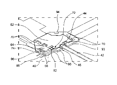
In the exemplary embodiment of Figures 1 and 3, the feed cable 12 is a
coaxial cable having exposed at its terminal end 42 a signal conductor, such
as
the inner conductor 44 shown in Figure 3, and a ground conductor, such as the
braided shield 46 shown in Figure 3. As shown in Figure 1, the cover 16 in the
first embodiment includes a walled cutaway 48 dimensioned to provide access to
the terminal end 42 for attachment of the inner conductor 44 and the braided
shield 46. Adhesive (not shown) may be employed at the base of each wall of
the walled cutaway 48 in order to maintain the water-resistance of the cover
16.
Referring to Figure 3, the inner conductor 44 is electrically connected to a
feed-signal PCB 50 and the braided shield 46 is electrically connected to the
radiator PCB 18 (a portion of which is shown in Figure 3). In the first
embodiment, the feed-signal PCB 50 is disposed beneath the cover 16 (not
shown in Figure 3) of the antenna 10 for feeding the signal received from the
feed cable 12 to the radiator PCB 18.
Referring to Figures 3 and 4, the feed-signal PCB 50 includes a top side
52, a backside 54 (not directly visible in Figures 3 and 4) that is parallel
and
spaced apart from the top side 52 so as to define a feed-signal PCB 50 plane
therebetween, and includes an edge 56 defined around the perimeter of the
insulating dielectric material 58 of the feed-signal PCB 50.
7
Date Recue/Date Received 2021-05-06
A feeding circuit is defined by electrically conductive material 60 that in
the
first embodiment is made of copper printed on the feed-signal PCB 50 so as to
include a coplanar waveguide implemented by a signal feed, such as the signal-
feed track 62 shown in Figures 3 and 4, that is separated from a signal
return,
such as the plurality of signal-return tracks 66 shown in Figures 3 and 4, by
a
dielectric area 64 that is non-conductive. In the first embodiment, the
plurality of
signal-return tracks 66 effectively surround the signal-feed track 62 while
being
separated from the signal-feed track 62 by the dielectric area 64. The signal-
feed track 62 and the signal-return tracks 66 are coplanar to and spaced apart
from each other on the top side 52 of the feed-signal PCB 50.
The signal-feed track 62 includes a plurality of signal-feed projections 68
that interfit with, while remaining spaced apart from, a corresponding
plurality of
signal-return projections 70 of the plurality of signal-return tracks 66. Such
interfitting projections 68 and 70 advantageously provide impedance matching
in
the UHF band, including its UHF sub-bands.
The conductive material 60 also defines an impedance-matching circuit 70
in shunt mode that is particularly effective for the VHF band. The impedance-
matching circuit 72 includes a meandering trace 74 and a pair of SMT (surface
mount) resistor pads 76 for receiving a SMT resistor 78 that provides a
resistance connected in series with the meandering trace 74. At a proximal end
80 of the meandering trace 74 is one pad 76 for receiving one end of the SMT
resistor 78. The other pad 76 is at the signal-feed track 62 on the other side
of a
trace-free gap 82 defined between the pads 76. The distal end 84 of the
meandering trace 74, opposite the proximal end 80, is at the edge 56 of the
feed-
signal PCB 50. Between the proximal and distal ends 80 and 84 of the
meandering trace 74 is at least one switchback 86 that completes at least one
turn of 180 degree.
As best seen in Figure 3, along the edge 56 at the distal end 84 of the
meandering trace 74 is an electrically conductive edge connection 88 for
8
Date Recue/Date Received 2021-05-06
electrically connecting the meandering trace 74 to the radiator-return track
40 of
the radiator PCB 18. Along the edge 56, the edge connection 88 lies between
non-conductive dielectric material 58 portions. Such edge-plating of the edge
connection 88 places the impedance-matching circuit 72 in shunt mode relative
to the signal-feed track 62.
Also shown in Figure 3 are ground-return edge connections 90 along the
edge 56 that connect the plurality of signal-return tracks 66 to the radiator-
return
track 40 and to electrical ground provided by its connection to the braided
shield
46.
In the first embodiment, the edge connection 88 and the ground-return
edge connections 90 are made of copper by edge plating (or sideplating) and
are
electrically connected to the radiator-return track 40 by soldering, welding,
or
similar.
Still referring to Figure 3, the inner conductor 44 of the first embodiment is
electrically connected to the signal-feed track 62 of the feed-signal PCB 50
and
the braided shield 46 is electrically connected to the radiator-return track
40 of
the radiator PCB 18. While not directly visible in Figures 3 and 4, in the
first
embodiment there is no conductive material 60 on the backside 54 of the feed-
signal PCB 50 such that the backside 54 of the feed-signal PCB 50 is circuit-
free.
With reference to Figures 2 and 3, when the feed-signal PCB 50 is placed
adjacently parallel to the radiator PCB 18, the electromagnetic signal
received
from the inner conductor 44 onto the signal-feed track 62 is thereafter
capacitively coupled via the dielectric material 58 to the radiator track 36,
including especially to a portion 92 (Figure 2) of the radiator track 36
adjacent to
the signal-feed track 62. In the first embodiment, the electromagnetic signal
at
the signal-feed track 62 is suitably impedance matched by the impedance
matching circuit 72 and the plurality of interfitting projections 68 and 70
for
capacitive coupling to the radiator track 36.
9
Date Recue/Date Received 2021-05-06
Referring to Figures 2 to 4, the antenna 10 also includes a pair of
conductive islands 94 on the feed-signal PCB 50, including at its edge 56, and
on
the radiator PCB 18, respectively. The islands 94 provide additional
mechanical
stability when connected to each other, such as by soldering, welding, or
similar,
and do so advantageously without degrading the electromagnetic performance of
the antenna 10.
Referring to Figure 5, the antenna 10 is suitable for being mounted indoors
at a ceiling 96 of a building structure 98. The mounting holes 32 (Figures 1
and
2) of the radiator PCB 18 are dimensioned to receive fasteners, such as the
bolts
100 shown in Figure 5. In the exemplary mounting configuration of Figure 5,
the
bolts 100 pass through the radiator PCB 18 at the mounting holes 32 and pass
through the ceiling 96 to corresponding nuts 102 fastened to the bolts 100
above
the ceiling 96. The feed cable 12 also passes through an aperture in the
ceiling
96 into a plenum space 104 of the building structure 98 above the ceiling 96.
Typically, the feed cable 12 includes a connector 106 to connect to a common
signal-feed source (not shown) of a distributed antenna system.
In the exemplary mounting configuration of Figure 5, the antenna 10,
including its cover 16, is entirely beneath the ceiling 96 and a separation
108
between the antenna 10 and the building structure, including its ceiling 96,
is
maintained by spacers 110 coupled to the bolts 100. In some embodiments (not
shown), however, the spacers 110 are excluded and the radiator PCB 18 is
mounted with its top side 20 flush against or otherwise adjacently in contact
with
the ceiling 96. In embodiments not employing the spacers 110, an additional or
larger recess or aperture in the ceiling 96 is required to permit the cover 16
to
protrude into the ceiling 96 or through the ceiling 96 into the plenum space
104.
While not directly visible in Figure 5, the antenna 10 in the first
embodiment is painted or otherwise coated with a fire-resistant coating 112.
In
the first embodiment, the cover 16 prevents the fire-resistant coating 112
from
Date Recue/Date Received 2021-05-06
ingressing into the interior of the enclosure 14 (Figure 1) when the fire-
resistant
coating 112 is applied.
As can be readily seen in Figure 5, the antenna 10 of the first embodiment
is a low-profile, planar antenna 10 having a minimal vertical height. The
circuit-
free backside 22 of the radiator PCB 18 and the fire-resistant coating 112 of
a
selected colour, such as white or off-white, and selected sheen, such as a
matte
finish, advantageously provide an unobtrusive appearance to the mounted
antenna 10 that is aesthetically pleasing.
Referring to Figure 6, the antenna 10 is particularly suitable for
transmitting electromagnetic radiation in multiple frequency bands, including
in
the frequency range of 132 MHz to 174 MHz of the VHF band, in the frequency
range of 350 MHz to 520 MHz of the UHF band, and in the frequency range of
698 MHz to 960 MHz (which can be referred to as the "700/800 band"). As can
be seen in the graph 114 shown in Figure 6, the voltage standing wave ratio
(VSWR) of the antenna 10, measured in a free-space environment, is less than
2.0 at frequencies within the multiple frequency bands, including at the low
frequency of 132 MHz.
In the first embodiment, no more than four bolts 100 are needed to mount
the antenna 10 to the ceiling 96, thereby minimizing the generation of passive
intermodulation (PIM) that could degrade antenna 10 performance. Also, the
radiator PCB 18, feed-signal PCB 50, feed cable 12, and connector 106 have
low-PIM performance ratings in the first embodiment. Accordingly, the antenna
10 according to the first embodiment is a low-PIM antenna 10.
Method of Assembly
Referring to Figures 1 to 4, the antenna 10 in the first embodiment can be
assembled by an exemplary method of assembly in which a first step is to
attach,
such as by soldering, the SMT resistor 78 onto the resistor pads 76.
Typically,
11
Date Recue/Date Received 2021-05-06
the resistance value of the SMT resistor 78 is selected for optimal antenna 10
performance.
Before or after the SMT resistor 78 is attached, the feed-signal PCB 50 is
attached to the radiator PCB 18. Attaching the feed-signal PCB 50 to the
radiator PCB 18 typically involves aligning the feed-signal PCB 50 according
to
silkscreened indicators on the radiator PCB 18; alignedly positioning the feed-
signal PCB 50 against the radiator PCB 18; attaching, such as by soldering or
welding, the conductive islands 94 to each other via a connecting trace at the
edge 56; and connecting, such as by soldering or welding, the feed-signal PCB
50 at its edge connection 88 and ground-return edge connections 90 to the
radiator-return track 40 of the radiator PCB 18.
Before or after the feed-signal PCB 50 is attached to the radiator PCB 18,
the cover 16 at its grommet 26 is placed over the unconnectorized terminal end
42 of the feed cable 12; the terminal end 42 of the feed cable 12 is
positioned
proximate to the feed-signal PCB 50; the braided shield 46 is electrically
connected, such as by soldering or welding, to the radiator-return track 40;
the
inner conductor 44 is electrically connected, such as by soldering or welding,
to
the signal-feed track 62; an adhesive, such as a double-sided adhesive tape
(not
shown), is applied to the flange 24 of the cover 16; and the cover 16 at its
grommet 26 is slid along the feed cable 12 until the cover 16 is positioned
over
the feed-signal PCB 50 and against the radiator PCB 18. Upon curing of the
adhesive, the antenna 10 can be used, including being mounted for use.
Thus, there is provided an antenna for use in a distributed antenna
system, the antenna comprising: (a) a feeding circuit disposed on a first side
of a
first dielectric defining an edge perpendicular to the first side, the feeding
circuit
comprising a coplanar waveguide comprising a signal feed and a signal return
coplanar with and interfittedly apart from the signal feed; (b) a radiator
circuit
disposed on a second side of a second dielectric, the radiator circuit
comprising a
monopole radiator and a radiator return copolanar with and spaced apart from
12
Date Recue/Date Received 2021-05-06
the monopole radiator, the first dielectric capacitively coupling the signal
feed to
the monopole radiator; and (c) an edge connection disposed along the edge for
electrically connecting the signal return to the radiator return.
While embodiments of the invention have been described and illustrated,
such embodiments should be considered illustrative of the invention only.
Thus,
the embodiments described and illustrated herein should not be considered to
limit the invention as construed in accordance with the accompanying claims.
13
Date Recue/Date Received 2021-05-06