Note : Les descriptions sont présentées dans la langue officielle dans laquelle elles ont été soumises.
CA 03113653 2021-03-12
WO 2020/051711
PCT/CA2019/051298
1
EFFICIENT ELECTRICITY CONVERSION FOR HARVESTING ENERGY FROM
LOW VOLTAGE SOURCES
FIELD
[0001] The application relates to systems and methods for converting
energy harvested from low voltage sources.
BACKGROUND
[0002] Many sources of energy that can be harvested are in the form
of
electricity or can be readily converted to it. However in many practical
situations,
these electricity sources are either weak, with too high or too low a voltage,
or
with certain other issues. Consequently, they are rarely directly useful to
low
power electronic devices, for example in wireless sensor networks and Internet
of
Things (IoT) applications, where a relatively steady supply of a direct
current
(DC) voltage of a few volts may be required.
[0003] It would be advantageous to have systems and methods for
efficiently and robustly converting low voltage DC electricity, such as from a
thermo-electric generator (TEG), for example a thermopile, into a usable form,
for example for use by wireless sensor networks and IoT applications.
[0004] An element in a system that turns low voltage DC electricity
from a
TEG into a usable form is a step-up DC-DC converter. A step-up DC-DC converter
converts a low voltage DC input to a higher voltage DC output.
[0005] There are various step-up DC-DC converters for TEG energy
harvesting available on the market. Many of these schemes rely on an
oscillator
to do the conversion.
[0006] Examples include those proposed in the following three
references:
a. EnOcean GmbH, ECT 310 Perpetuum,
https://www.enocean.com/en/enocean modules/ect-310-perpetuum/.
CA 03113653 2021-03-12
WO 2020/051711
PCT/CA2019/051298
2
b. Linear Technology Corporation, LTC3108 - Ultralow Voltage Step-Up
Converter and Power Manager, http://www.linear.com/product/LTC3108.
c. Dario GrgiC, To!gay Ungan, Milo g KostiC, and Leonhard M. Reindl,
"Ultra-Low Input Voltage DC-DC Converter for Micro Energy Harvesting,"
PowerM EMS 2009, pp. 265268, Washington DC, USA, December 1-4, 2009.
[0007] Each of the three schemes introduced above works in a certain
input
range and at a relatively low efficiency. Their turn-on source conditions and
efficiencies are summarized in Table 1 below, where VOC is the open-circuit
voltage of the TEG device and RTEG is the internal resistance (also known as
the
source resistance) of the device. The turn-on source conditions for this
example
include turn-on voltage and RTEG. The turn-on voltage is the minimum voltage
required from the source before the DC-DC converter starts to produce a DC
output voltage with an absolute value greater than that of the input.
Table 1. Turn-on source conditions and efficiencies of existing schemes
ECT310 by LTC3108 by Linear Dario GrgiC
EnOcean Technology et al.
Turn-on source VOC=20mV & VOC=50mV & VOC=10mV
condition RTEG=2Q RTEG=20Q
&
Or Or
DT(- ((l
Efficiency 30% 20 - 40% < 18%
Note that, for Scheme Dario GrgiC et al., VOC at RTEG = 50Q is derived from
information provided in the abstract of the third reference: Vcc = 6 mV
(closed-
circuit input voltage) and input power of 490 nW.
SUMMARY
[0008] A DC-DC converter and method are provided for converting a low
voltage DC input to a higher voltage DC output. The DC-DC converter has an
CA 03113653 2021-03-12
WO 2020/051711
PCT/CA2019/051298
3
oscillator with a first relatively voltage sensitive and relatively low power
transistor and a second relatively voltage insensitive and relatively high
power
transistor, the oscillator producing an AC signal from the low voltage DC
input.
The inclusion of the voltage sensitive transistor allows the oscillator to
turn on at
a relatively low voltage. The inclusion of the higher power transistor allows
the
oscillator to operate at a higher power once it turns on. The DC-DC converter
can be used for converting energy harvested from low voltage sources.
[0009] According to one aspect of the present invention, there is
provided a
DC-DC converter for converting a low voltage DC input to a higher voltage DC
output, the DC-DC converter comprising: an oscillator comprising a first
relatively
voltage sensitive and relatively low power transistor and a second relatively
voltage insensitive and relatively high power transistor, the oscillator
producing
an AC signal from the low voltage DC input; a transformer for converting the
AC
signal produced by the oscillator to a higher voltage AC signal; a voltage
doubling rectifier for converting the higher voltage AC signal to the higher
voltage DC output; wherein first and second transistors of the oscillator are
such
that the oscillator is initially turned on when the low voltage DC input is
sufficiently
high to start the oscillator initially using only the first relatively high-
sensitivity low
power transistor, and the second transistor turns on when the voltage on a
secondary side of the transformer exceeds the turn-on voltage of the second
transistor.
[0010] Optionally, the first transistor is a JFET device and the
second
transistor is a MOSFET device.
[0011] Optionally, the second transistor has a relatively lower on-
resistance
RDS(on) than the first transistor.
[0012] Optionally, the DC-DC converter further comprises an adaptive
clamping mechanism that ensures a suitable bias for the first transistor under
practical source and load conditions.
CA 03113653 2021-03-12
WO 2020/051711
PCT/CA2019/051298
4
[0013] Optionally, the adaptive clamping mechanism comprises a
capacitor
connected between the output of a secondary of the transformer and the gate of
the first transistor, and a gate-source PN junction of the first transistor.
[0014] Optionally, a turns-ratio of the transformer is selected for a
particular source and load combination.
[0015] Optionally, the transformer has an adjustable turns-ratio.
[0016] Optionally, the transformer has taps and a selector for
selecting between a plurality of turns-ratios.
[0017] Optionally, the selector is one of: mechanical; electronic and
operated manually; electronic and operated by an independent control module;
electronic whose state is automatically determined based on the current source
and load conditions.
[0018] Optionally, the voltage doubling rectifier has a first stage
formed of
a first capacitor and the gate-source junction of the first transistor, and a
second
stage formed of a diode and a second capacitor.
[0019] Optionally, the diode is connected between the first capacitor
and
the second capacitor, the diode connected to permit current flow in a
direction
from the second capacitor towards the first capacitor.
[0020] Optionally, the voltage doubling rectifier has a first stage
formed of
the capacitor of the adaptive clamping mechanism and the gate-source junction
of the first transistor, and a second stage formed of a diode and another
capacitor.
[0021] Optionally, the diode is connected between the capacitor of
the
adaptive clamping mechanism and the another capacitor, the diode connected to
permit current flow in a direction from the another capacitor to the capacitor
of
the adaptive clamping mechanism.
CA 03113653 2021-03-12
WO 2020/051711
PCT/CA2019/051298
[0022] Optionally, the DC-DC converter further comprises an output
isolation switch.
[0023] Optionally, the output isolation switch comprises a transistor
for
isolating the load from the remainder of the DC-DC converter when there are
5 harsh load conditions causing output terminals of the DC-DC converter to
be
either shorted or driven, and a resistor for allowing a leakage current
following
removal of the harsh load conditions such that the first transistor can start
up.
[0024] Optionally, the DC-DC converter further comprises an output
voltage
limiter.
[0025] According to another aspect of the present invention, there is
provided power supply comprising: a low voltage source; the step-up converter
as described herein.
[0026] Optionally, the low voltage source is a thermo-electric
generator.
[0027] According to another aspect of the present invention, there is
provided a method of converting a low voltage DC input to a higher voltage DC
output, the method comprising: producing an AC signal from the low voltage DC
input using an oscillator comprising a first relatively voltage sensitive and
relatively low power transistor and a second relatively voltage insensitive
and
relatively high power transistor, by starting up oscillation of the oscillator
when
the low voltage DC input is sufficiently high to start the oscillator
initially using only
the first relatively high-sensitivity low power transistor, and turning on the
second
transistor when the voltage on a secondary side of the transformer exceeds the
turn-on voltage of the second transistor; converting the AC signal produced by
the oscillator to a higher voltage AC signal with a transformer; voltage
doubling
rectifying the higher voltage AC signal to produce the higher voltage DC
output.
[0028] Optionally, the first transistor is a JFET device and the
second
transistor is a MOSFET device.
CA 03113653 2021-03-12
WO 2020/051711
PCT/CA2019/051298
6
[0029] Optionally, the method further comprises performing adaptive
clamping to ensure a suitable bias for the first transistor under practical
source
and load conditions.
[0030] Optionally, the method further comprises selecting a turns-
ratio
of the transformer for a particular source and load combination.
[0031] Optionally, selecting a turns-ratio of the transformer
comprises
one of: mechanically selecting one of a plurality of possible turns-ratios;
electronically selecting one of a plurality of possible turns-ratios based on
manual input; electronically selecting one of a plurality of possible turns-
ratios operated by an independent control module; electronically selecting
one of a plurality of possible turns-ratios automatically determined based on
the current source and load conditions.
[0032] Optionally, wherein the second transistor has a relatively
lower on-
resistance RDS(on) than the first transistor.
BRIEF DESCRIPTION OF THE DRAWINGS
[0033] Embodiments of the disclosure will now be described with
reference
to the attached drawings in which:
FIG. 1 is a circuit diagram of a DC-DC converter provided by an
embodiment of the invention; and
FIG. 2 is a flowchart of a method of performing DC-DC conversion
provided by an embodiment of the invention.
DETAILED DESCRIPTION
[0034] It would be desirable to have a DC-DC converter design with
the
following properties:
turn-on VOC that is less than about 25 mV at a source
resistance of about 50 Q;
CA 03113653 2021-03-12
WO 2020/051711
PCT/CA2019/051298
7
a maximum efficiency that is higher than 40%; and
features the ability to choose different trade-offs between the
turn-on voltage and the output driving capability.
[0035] These properties cannot be simultaneously realized by any of
the
three above-referenced schemes for reasons detailed below.
[0036] To ensure the oscillations start with a weak input power -
meaning
low source VOC and/or high RTEG , the driver in the oscillator should be able
to
provide a large gain, but not necessarily a big driving power. On the other
hand, once the oscillation has been established and stable, a large driving
power is needed to achieve the needed power throughput and a high efficiency
of the overall converter.
[0037] The second referenced scheme uses a proprietary depletion-mode
MOSFET as the driver. With a claimed minimum RDS(on) of only 0.5 Q, it is
capable of providing a large power throughput. RDS(on) of a FET (MOSFET or
JFET) is defined as the resistance between Drain and Source terminals at a
certain VGS I being the voltage across Gate and Source terminals. However, the
transistor's "common source trans-conductance" gain around VGS = 0 V,
namely gm and also known as lyfsl, is only around 10 mC3 as per Applicant's
measurement. gm of a FET (MOSFET or JFET) is defined as gm = AIDs/AVGs i.e.,
ratio of the resultant output current increment to the input voltage
increment.
As a result of the low gm of the MOSFET, this scheme needs a relatively high
turn-on power.
[0038] In contrast, the third referenced scheme adopts a high-gain
JFET
(BF862) as the driver, with a typical gm of 45 mC3 ; therefore, the third
referenced scheme can start on a very weak input power. However, this
transistor's minimum RDS(on), at VGS = 0 V, is about 30 Q which is much
larger than that of the transistor used in the second referenced scheme.
CA 03113653 2021-03-12
WO 2020/051711
PCT/CA2019/051298
8
[0039] In general, it is difficult to find a driving transistor with
a gm high
enough and at the same time an RDS(on) low enough to deliver the mentioned
properties, if one even exists.
[0040] In accordance with an embodiment of the invention, a step-up
DC-
DC converter is provided. In some specific implementations, which may depend
for example on specific component choices and the inclusion of optional
features, the provided DC-DC converter meets the above requirements and
outperforms the three referenced existing schemes.
[0041] In a very specific realization, the DC-DC converter includes a
transformer set or setable at a turns-ratio of 1:100, and the provided DC-DC
converter can reliably start at VOC = 22.8 mV and RTEG = 50 Q, and can
achieve a maximum efficiency of about 44%.
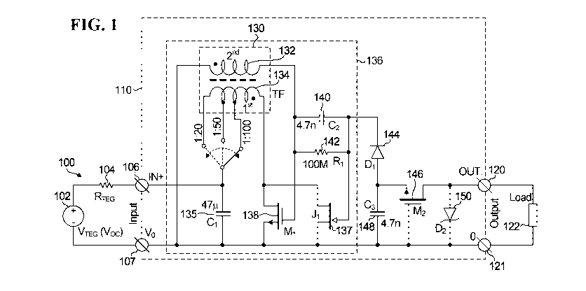
[0042] Referring now to FIG. 1, shown is circuit diagram of a power
supply and load provided by an embodiment of the invention. In FIG. 1, a low
voltage source is generally indicated at 100, which is connected via positive
and
negative input terminals 106,107 to the provided step-up converter circuit
which is generally indicated at 110, which in turn is connected via positive
and
negative output terminals 120,121 to a load 122. The low voltage source 100
and the DC-DC converter 110 together form the power supply that powers the
load 122.
[0043] The low voltage source 100 is modelled as a voltage source 102
that produces an input voltage VTEG on input terminal 106 relative to VO on
input terminal 107, and an input resistance RTEG 104.
[0044] The schematic of the step-up DC-DC converter 110 will be
described in detail followed by a description of its functionality. A
capacitor Cl
135 is connected across the input terminals 106,107 to reduce the impact of
the
fluctuating load current and to suppress potential interference. Shown is a
transformer 130 having a primary winding 134 and a secondary winding 132.
The polarity configuration of the transformer windings is indicated by the
CA 03113653 2021-03-12
WO 2020/051711
PCT/CA2019/051298
9
phasing dots. In the illustrated example, the primary winding 134 has a
selectable number of turns such that the turns ratio between the primary and
the secondary windings 134,132 is adjustable. In some embodiments, a
transformer with a primary winding having a fixed number of turns is employed.
[0045] One terminal of the primary winding 134 is connected to input
terminal 106 and the other terminal of primary winding 134 is connected to the
drains of two transistors of a dual-transistor oscillator 136, the two
transistors
including a low power startup transistor J1 137, and a higher power transistor
M1 138. One terminal of the secondary winding 132 is connected to VO, and
the other is connected to gate of transistor M1 138 and to gate of transistor
J1
137 via capacitor C2 140 connected in parallel with resistor R1 142.
[0046] The output of the parallel circuit formed by C2 140 and R1 142
is
connected to the cathode of a diode D1 144. The anode of D1 144 is connected
to the source of transistor M2. The anode of D1 144 is also connected via a
capacitor C3 to VO. The gate of transistor M2 146 is connected to VO, and
drain
of transistor M2 146 is connected to negative output terminal 120. Finally, an
optional Zener diode D2 150 is shown connected between drain of transistor M2
and VO, equivalently across the output terminals 120,121.
[0047] In the embodiment illustrated, the dual-transistor oscillator
136
includes the two transistors M1 and J1, and also the transformer, C1, C2 and
R1. However it should be understood different implementations are possible, so
long as the transistor oscillator includes two transistors, one of which has a
low
turn-on voltage and low power, and the other of which has relatively high turn-
on voltage and high power.
[0048] Example component values and types are indicated in FIG. 1. It
should be clearly understood that these are for the purpose of example only.
The provided circuit is suitable to transform voltages from a TEG source,
typically in the 10 to 20 mV range, to a higher voltage suitable for portable
electronics, for example 2 - 5 V. The example component values and types are:
CA 03113653 2021-03-12
WO 2020/051711
PCT/CA2019/051298
Cl 47 pF; for example ceramic, thin film, polyester, or electrolytic
Transformer 134,132 has turns ratios selectable between 1:20, 1:50
and 1:100. In a specific implementation, the transformer has characteristics
similar to that of Coilcraft's LPR6235-253PMR, LPR6235-123QMR or LPR6235-
5 752SMR.
Ml: NTUD 3170NZ
J1: BF862 or 2SK932
C2: 4.7 nF, for example ceramic
R1: 100 MQ
10 Dl: 1N649-1 or similar. In another specific example, the gate
source junction of another JFET such as 2SK932 is used for Dl;
C3: 4.7 nF ceramic
M2: NTUD 3170NZ
D2: ESD9R3.3S
[0049] The illustrated step-up converter circuit includes a number of
specific features the functionality of which is detailed further below. For
brevity,
in the description that follows components will be identified by their
component
names only.
a. a dual-transistor oscillator 136 formed of at least transistors J1 and
M1
b. an adaptive clamping bias mechanism (C2 and J1) for transistor J1
c. an adjustable turns-ratio transformer
d. a voltage doubling rectifier (C2, J1, D1, and C3)
CA 03113653 2021-03-12
WO 2020/051711
PCT/CA2019/051298
11
e. an output isolation switch (M2 and R1),
f. an output voltage limiter (D2).
Other embodiments are possible that do not include all these features. For
example, in some embodiments, the output voltage limiter is included if the
output is to be limited to around 6 V; otherwise, the built-in protection
diodes
between gate and source of M2 can also provide an overvoltage protection
though at a slightly higher potential, of about 8 V. As another specific
example,
there is no need for resistor R1 in some implementations, for example if the
load
is not capacitive.
Dual-transistor Oscillator
[0050] Since transformers work on AC voltages, an oscillator is
provided to
convert a DC input voltage to an AC voltage. While existing schemes use a
single transistor in the oscillator, the provided circuit features a dual-
transistor
oscillator 136 having start-up transistor J1 for low power start-up and power
transistor M1 for high power throughput.
[0051] The dual transistor oscillator addresses the difficulty of
finding a
single transistor that has a high gain and a low RDS(on) simultaneously.
[0052] J1 is a JFET device with a high sensitivity, meaning gm or
common
source trans-conductance being high compared to that of Ml, to ensure a
reliable start-up of the oscillation even if the input power is weak. In this
case,
M1 may have little effect; M1 has comparatively low sensitivity such that it
stays off as long as the peak of the induced voltage at the secondary side of
the
transformer is lower than its VGS(th), for example of about 0.7 V. VGS(th) of
a
MOSFET such as M1 is a threshold voltage defined as the VGS at which the
transistor starts to conduct. Note that in the illustrated example, M1 is an
enhancement-mode MOSFET. Therefore when the input power is weak, the
converter operates on J1 only and is not capable of providing a large power
throughput, but there is not much input power to be passed on anyway.
CA 03113653 2021-03-12
WO 2020/051711
PCT/CA2019/051298
12
[0053] As the input power increases, so does the induced voltage
at
the secondary side of the transformer. When exceeding VGS(th) of M1 (¨ 0.7
V), this voltage turns on the latter, whose RDS(on) (about 1-3 Q for the
specific
component illustrated) is much smaller than J1's. Therefore, the converter
with
both J1 and M1 in operation is capable of providing a larger power throughput.
[0054] If for whatever reason the input power drops low again, so
will
the induced voltage at the transformer's secondary side. This will
automatically
turn M1 off.
Adaptive Clamping Mechanism
An adaptive clamping mechanism is provided to ensure a suitable bias for the
start-up transistor J1 under practical source and load conditions.
[0055] It is beneficial to bias J1 so that it operates around the
vicinity of
its VGS(off), for example of around -0.8 V for transistor BF862 as J1.
VGS(off)
of a JFET such as J1 is the VGS at which the transistor is said to be cutoff.
And,
its VGS should not go positive normally.
[0056] In the described embodiment, an adaptive clamping mechanism
consisting of C2 and the Gate-Source PN junction of J1 keeps J1 suitably
biased
all the time. The voltage across C2 follows the peak positive voltage of the
transformer's secondary side and equals the latter minus the forward voltage
drop of J1's Gate-Source PN junction. When the AC voltage of transformer's
secondary side increases for whatever reason, C2 is charged to a higher
voltage
through the Gate-Source PN junction of J1. This keeps the PN junction reverse
biased most of the time. On the other hand, if the AC voltage of the
transformer's secondary side decreases, C2 is not charged because the PN
junction of J1 stays reverse biased. Then, C2 discharges through D1 to the
load
and to a less extent through R1, until the voltage across C2 is low enough so
that
the aforementioned charging process resumes.
Adjustable turns-ratio Transformer
CA 03113653 2021-03-12
WO 2020/051711
PCT/CA2019/051298
13
[0057] The transformer 130 transforms the input AC voltage to a
higher
AC voltage with less current such that when the higher AC voltage is converted
back to DC, a step-up in voltage has been achieved. The inclusion of a
transformer with an adjustable turns-ratio enables optimization or
improvement of output power and efficiency. For different source and load
conditions, the optimal turns-ratio of the transformer, at which the step-up
DC-DC converter can deliver a maximum possible power at high efficiency, is
different. In general, a lower turns-ratio is preferred for higher input
voltages
and heavier loads, and vice versa.
[0058] In some embodiments, the transformer with adjustable turns-
ratio is implemented using one of:
providing transformers of different fixed turns-ratios for
each specific application to choose from and install in the target system;
or
incorporating a transformer with taps and a selector, as shown in
FIG. 1. This selector can be, in an ascending order of complexity,
- simply mechanical,
- electronic and operated manually,
- electronic and operated by an independent control module, or
- electronic whose state is automatically determined based on the
current source and load conditions.
[0059] For turns-ratios of 1:20 and 1:50, the source will have to
provide
more power than in the case with a 1:100 turns-ratio transformer in order for
the
step-up DC-DC converter to turn on. For example, the turn-on VOC of the
circuit
of FIG. 1 with source resistance RTEG = 50 Q is 22.8, 37.6, and 85.6 mV for
transformer's turns-ratios of 1:100, 1:50, and 1:20, respectively. If the
source
CA 03113653 2021-03-12
WO 2020/051711
PCT/CA2019/051298
14
resistance RTEG is reduced to 5 Q, these figures decrease to 10.0, 17.2, and
38.5 mV, respectively.
Voltage Doubling Rectifier
[0060] The output AC voltage of the transformer is converted back to
DC in
a voltage doubling rectifier. In the illustrated example, this is formed of
C2, J1,
D1, and C3. The output DC voltage is twice the peak AC oscillation voltage
less
the forward voltage drops of D1 and the Gate-Source PN junction of J1.
Advantageously, in addition to providing the adaptive clamping function
discussed above, C2 and the Gate-Source PN junction of J1 also acts as the
first
stage of the voltage-doubling rectifier. The second stage consists of D1 and
C3.
This multiplexing strategy not only reduces component count but also reduces
overhead power that would be consumed if a separate circuit were implemented
to fulfil the function of the rectifier's first stage.
[0061] In other embodiments, a different rectifier, that is not
necessarily a
doubling rectifier, is used.
Output Isolation Switch
[0062] To be practical, a step-up DC-DC converter should be robust
enough, i.e., it should be able to start and maintain oscillation even if the
output is shorted or driven. This is the case when, for example, the converter
is
used to charge a large capacitive load, such as a supercapacitor. This is
expected to happen very often because such energy harvesting devices are
most probably used to provide power to wireless sensors in a building and
these
sensors sleep most of the time and wake up intermittently to do the
measurement and transmission before going back to sleep again. Given the low
duty-cycle and impulsive nature of the load, a buffering supercapacitor is a
perfect choice in this context. When a supercapacitor is connected to a step-
up
DC-DC converter, the latter's output can be virtually shorted when the
capacitor
has no or little charge in it, or driven when the input power disappears or
goes
low while the capacitor already has some charge in it.
CA 03113653 2021-03-12
WO 2020/051711
PCT/CA2019/051298
[0063] As a result, there is a harsh load/output condition, for
example
when the output is shorted or driven, a step-up DC-DC converter without an
output isolation switch will not start or maintain oscillation normally. And,
the
oscillation may not resume after the harsh output condition is removed.
5 [0064] In the described embodiment, a simple output isolation
switch is
provided to effectively isolate the converter from harsh load conditions, so
that the device can start and operate normally even if the output is shorted
or driven. The switch is composed of transistor M2 and resistor R1. With a
weak input power or during start up, the "pre-output" voltage, across C3, is
10 lower than the VGS(th) of M2, M2 being an enhancement-mode MOSFET.
Therefore, M2 is off, isolating the converter from the load. This assures a
normal start up whatever the load condition is. If the load becomes shorted
or too heavy during operation, the significant amount of current it draws
drags down the output voltage to below the VGS(th) of M2. As a result, the
15 latter will turn off, preventing the oscillation from being ceased. Another
scenario is that, when the input power disappears and the load
supercapacitor has already accumulated some significant voltage, this
voltage can, through the forward-biased built-in diode in M2 (even if M2 is
off) and the reverse leakage of D1, charge C2 to a high enough voltage that
keeps J1 off when the input power resumes. This prevents the oscillation
from starting. This problem is resolved by introducing a very small leakage
device R1. This prevents the voltage across C2 from going too high, and the
power loss it incurs is proven to be negligibly small.
Output voltage limiter (D2)
[0065] Some embodiments features an output voltage limiter. The
circuit of FIG. 1 includes Zener diode D2 150 which serves this purpose. For
whatever reason if the load voltage exceeds an allowable value, an
appropriately chosen D2 150 will conduct and bring down the load voltage.
As a result, the load voltage will always be less than the Zener breakdown
value of D2 150.
CA 03113653 2021-03-12
WO 2020/051711
PCT/CA2019/051298
16
[0066] Referring now to FIG. 2, shown is a flowchart of a method of
converting a low voltage DC input to a higher voltage DC output provided by an
embodiment of the invention. The method begins in block 200 with producing an
AC signal from the low voltage DC input using an oscillator comprising a first
relatively voltage sensitive and relatively low power transistor and a second
relatively voltage insensitive and relatively high power transistor, by
starting up
oscillation of the oscillator when the low voltage DC input is sufficiently
high to start
the oscillator initially using only the first relatively high-sensitivity low
power transistor
, and turning on the second transistor when the voltage on a secondary side of
the transformer exceeds the turn-on voltage of the second transistor. The
method continues in block 202 with converting the AC signal produced by the
oscillator to a higher voltage AC signal with a transformer. The method
continues in block 204 with rectifying the higher voltage AC signal to produce
the
higher voltage DC output.
[0067] Note that any combination of the features described in the context
of the embodiment of FIG. 1 can also be included as method steps added to the
method of FIG. 2. For example, in some embodiments, the method further
involves performing adaptive clamping to ensure a suitable bias for the first
transistor under practical source and load conditions.
[0068] In some embodiments, the method also includes selecting a
turns-ratio of the transformer for a particular source and load combination.
[0069] Selecting a turns-ratio of the transformer may be performed,
for
example, using one of:
mechanically selecting one of a plurality of possible turns-ratios;
electronically selecting one of a plurality of possible turns-ratios
based on manual input;
electronically selecting one of a plurality of possible turns-ratios
operated by an independent control module;
CA 03113653 2021-03-12
WO 2020/051711
PCT/CA2019/051298
17
electronically selecting one of a plurality of possible turns-ratios
automatically determined based on the current source and load conditions.
[0070] Numerous modifications and variations of the present disclosure
are
possible in light of the above teachings. It is therefore to be understood
that
within the scope of the appended claims, the disclosure may be practiced
otherwise than as specifically described herein.