Note : Les descriptions sont présentées dans la langue officielle dans laquelle elles ont été soumises.
CA 03113726 2021-03-22
WO 2020/115332
PCT/EP2019/084275
________________________________________________________________________
HERMETIC PACKAGING OF ELECTRONIC COMPONENTS
The present invention relates to the field of electronic devices, in
particular implantable
electronic devices, e.g. for bio-medical applications, and more particularly,
to hermetically
packaged electronic devices for bio-medical in vivo applications and methods
of packaging
electronic components for manufacturing such electronic devices.
BACKGROUND
Electronic devices are ubiquitously used and often required to function even
under harsh
environmental conditions. E.g., implantable electronic devices, such as chips,
are used in bio-
medical in vivo applications, e.g. for performing undertaking, controlling or
monitoring bodily
functions. Retinal implants are a particular example. Such implantable
electronic devices are
typically in direct contact with bodily fluids and tissues. Therefore,
electronic devices, and in
particular implantable electronic devices for bio-medical in vivo applications
should be
packaged in order to 1) protect the implanted device against whatever
impairment by the body's
aqueous environment, such as the intrusion of redox-active or corrosive
compounds into the
device, which may cause corrosion, damage or improper function of the
implanted device, and
2) protect the body against leakage of harmful products released from the
electronic device into
the body's tissues, or against other disadvantageous effects for the patient's
body, such as
.. mechanical friction by the implanted device in the body.
Prior art approaches for packaging implantable electronic devices typically
place the device in a
metal housing. In this known way of packaging, the package is much larger than
the original
chip, requiring larger incisions during implantation, thus resulting in a more
extensive woLmd
healing and inflammation processes. Furthermore, the larger the implant, the
larger the fibrous
encapsulation may be, resulting in a higher risk of local tissue irritation
for the patient during the
CA 03113726 2021-03-22
WO 2020/115332 2
PCT/EP2019/084275
lifetime of the implant. The proposed hermetic packaging of the present
invention is superior to
said prior art approaches in that it is small, e.g. substantially of a similar
size as or only slightly
larger than the original device size itself. Its small size enables a less
traumatic implantation and
a faster wound healing. As compared to prior art methods of enclosing
electronic devices each
individually in metal housings, the inventive method offers the advantage of
being applicable for
simultaneous processing of multiple electronic devices or components of the
same or different
kinds, and is largely substantially independent of the substrate or component
materials used.
Moreover, the packaging can be performed in a clean environment, e.g. in clean
room conditions
after processing of the electronic devices or components, and in this way
contamination and/or
damage can be avoided. Furthermore, the inventive packaging method offers an
exceptionally
good step coverage resulting in overlapping layers and uniform thickness of
the encapsulation,
which provide a good hermetic seal.
US 2015/0297136 Al describes an alternative method for packaging biomedical
devices, which
.. does not entail the inventive use of a removable layer as a temporary
barrier for protecting the
encapsulation layers from degradation during manufacturing. Due to its
different method of
processing, US 2015/0297136 Al does not enable a hermetic encapsulation with
only two layers
and necessarily requires the use of an additional coating to achieve a
hermetic seal. Specifically,
the inventive packaging method enables the provision of a hermetically sealing
double-layer
covering the entire electronic device, and in particular its side walls. Such
double-layered
structures are particularly advantageous for ensuring a hermetic seal, as
single layers may
comprise pin holes (i.e., microscopic defects), which may constitute entry
points for surrounding,
potentially corrosive, media. A second layer of material will close these pin
holes and secure the
hermetic sealing of the encapsulation. With prior art methods, it was not
possible to provide a
double-layered seal fully surrounding all sides of an electronic device,
mainly due to the fact that
electronic device needs to be fastened during coating, rendering some of their
surfaces
inaccessible. It was not until the provision of the inventive packaging
method, which involves
flipping of the device and using a removable layer such as photoresist as a
temporary protective
barrier, that it became possible to deposit conformal sealing materials on the
side walls from both
sides and therefore provide a double layered fully surrounding seal. In
addition, in contrast to the
packaged device described in US 2015/0297136 Al, the inventive packaging
method obviates
the need for sloped side walls of the device, and can be used with highly
conformal coatings that
are capable of coating straight and right-angled surfaces as commonly present
in biomedical
implants. Furthermore, US 2015/0297136 Al does not relate to retinal implants
or envisage the
use of a top coating, let alone a transparent top coating as described in the
present invention.
CA 03113726 2021-03-22
3
WO 2020/115332
PCT/EP2019/084275
It is an advantage of the inventive method and packaging that a reliable
hermetic encapsulation
with a reduced number of pinholes can be obtained with only two overlapping
encapsulation
layers and without the need for an additional embedding layer surrounding the
packaged chip.
US 2013/330498 Al and US 2011/039050 Al disclose an implantable medical device
comprising an electronic component being encapsulated by a packaging with
encapsulation
layers stacked onto each other, thus forming a multi-layer encapsulation.
SUMMARY
Inventive aspects relate to methods for hermetically packaging electronic
components for
manufacturing packaged electronic devices, e.g. implanted electronic devices
for bio- or bio-
medical in vivo applications and packaged electronic devices obtained by such
a method.
Advantageously, the packaging according to the invention provides an improved
hermetic
barrier, which preferably minimizes the interaction between the electronic
device or its
functional electronic component on the one hand and its environment on the
other hand, e.g.
the in vivo environment when implanted. Thereby, the inventive packaging
preferably 1) ensures
maintenance of the function of the electronic device under in vivo conditions,
e.g. by avoiding
improper function of the device, e.g. due to corrosion or short circuit
effects, and 2) protect the
body against leakage/leaching or diffusion of materials of the device's
electronic component into
the surrounding tissue when implanted, or against other adverse effects, such
as mechanical
friction of the implanted device in the body. Put differently, the hermetic
packaging
characterizing the present invention's device establishes a reliable barrier
against external factors.
More specifically, the invention may provide a bi-directional diffusion
barrier without affecting
the device by its in vivo environment and without diffusion of unphysiological
or non-
biocompatible materials of the electronic component into the tissue
surrounding the implanted
device. The advantageous properties of the inventive packaging are preferably
obtained by
providing layered encapsulation fully encapsulating the electronic component.
The resulting
packaged device exhibits at least partially overlapping layers embedding the
electronic
component to form a double layer structure, which is preferably obtained or
obtainable using the
inventive packaging method.
In a first aspect, the invention relates to an implantable packaged device
comprising an electronic
component and a hermetic package encapsulating the electronic component,
wherein said
packaging comprises a top and a bottom encapsulation layer, which least
partially overlap so as
to form a double layer structure. Preferably, the double layer structure at
least partially, more
CA 03113726 2021-03-22
4
WO 2020/115332
PCT/EP2019/084275
preferably fully, extends over and thereby covers the electronic component's
side walls. In this
way, the packaging of the device may advantageously provide a hermetic seal
for its electronic
component. As used herein, the terms "hermetic", "hermetically seal" and
"hermetic seal" means
impervious or essentially impervious to undesired external factors negatively
affecting the
device's function. That is, a "hermetic" seal or encapsulation preferably
shields the implantable
device from its environment, in particular the aqueous in vivo environment in
an effective way,
such that corrosion or whatever other functional impairment of the device is
preferably
minimized or avoided. Preferably, a "hermetic" seal or layer prevents the
ingress of bodily fluids
to the device. The term "hermetic" may further mean that the body is likewise
shielded from the
implanted device.
The packaged device is typically defined by side wall surfaces and by a top
and bottom surface.
The terms "top encapsulation layer" and "bottom encapsulation layer" are
typically meant to
cover ¨ at least partially ¨ the upper (top) surface of the electronic
component to be encapsulated
or the bottom surface of the electronic component. Thus, the "upper surface"
of the electronic
device is fully or partially covered by one or more layers, the outermost
thereof defining the top
surface of the packaged implantable device, whereas the bottom surface of the
electronic
component to be packaged is covered by one or more bottom layers, the
outermost thereof
defining the bottom surface of the packaged implantable device.
It is understood that the device may contain feedthroughs or holes for
communication with its in
vivo environment, e.g. by electrical stimulation of the surrounding cells or
tissues. The "upper
portion" of the packaged implantable device contains functional structures or
features allowing
the device to interact with its environment, e.g. by comprising stimulating or
recording electrodes
or photodiodes. The "top surface" of the implantable packaged device thereby
(partially) covers
its upper portion, whereas the "bottom surface" covers its lower portion. The
top surface or a
portion thereof may ¨ for some embodiments - expose a coating layer as the
outermost layer
being in contact with the environment. In terms of the production method to
provide a packaged
device according to the invention, it is noted that the production method is
characterized by
initial steps applying one or more encapsulating layer/s on the top surface,
while the bottom
surface is only thereafter established by applying one or more bottom
encapsulating layer/s.
In a second aspect, the invention provides an implantable system comprising
the hermetically
packaged device according to the invention.
In a third aspect, the invention relates to a packaging method for providing
or manufacturing an
implantable device, whereby the method comprises (a) providing at least one
electronic
component present on a substrate, (b) applying at least one top encapsulation
layer to an
CA 03113726 2021-03-22
WO 2020/115332
PCT/EP2019/084275
electronic component, and (c) applying at least one bottom encapsulation layer
to the electronic
component, wherein the top and bottom encapsulation layer at least partially
overlap so as to
form a double layer structure. Advantageously, the inventive method may allow
processing
multiple electronic components, such as electronic dies, simultaneously to
manufacture a
5 multitude of packaged electronic devices, which results in a cost-
effective and scalable
production process, especially for chip fabrication.
In a further aspect, which may also be an embodiment of the second aspect, the
invention relates
a method for packaging an electronic component to provide a packaged
implantable device, said
method comprising the steps of: (i) providing an assembly of at least one,
preferably a plurality
of electronic components separated from each other on a substrate by
introducing recesses into
an electronic component proto-structure, wherein adjacent electronic
components and their
common substrate support or define the recesses; (ii) applying at least one
top encapsulation
layer to an assembly, thereby coating the electronic components and lining the
recesses; (iii)
applying a removable layer to the assembly; (iv) partially removing the
removable layer, thereby
retaining a residual amount of the removable layer within lined recesses; (v)
optionally flipping
the assembly upside down; (vi) removing a) substrate, b) top encapsulation
layer and c) residual
amount of removable layer from the assembly's bottom side; and (vii) applying
at least one
bottom encapsulation layer to the assembly, wherein top and bottom
encapsulation layers are
applied so as to at least partially overlap, thereby forming a double layer
structure. According to
the inventive method, the top or upper side of the assembly is initially
processed by adding the
top encapsulation layer and the removable layer. Subsequently, the assembly is
preferably flipped
upside down (thus allowing the bottom side to be processed preferably from
below and, less
preferably, from above) to remove the substrate from the assembly's bottom
side, and the top
encapsulation layer below the removable layer within the recesses. Thereby, a
residual amount
of the removable layer is retained in each recess, which preferably protects
the top encapsulation
layer lining the sidewalls of the recesses against degradation. Subsequently,
the removable layer
is typically completely removed. Finally, the bottom encapsulation layer is
applied to the
assembly's bottom side and the sidewalls. Advantageously, the inventive method
¨ preferably by
flipping the assembly upside down during processing and retaining the
removable layer for
protection ¨ allows for a hermetic packaging based on stacked encapsulation
layers extending
over the electronic component's side walls, which enables improved hermetic
properties.
The methods according to the third and fourth aspect of the invention for
packaging an
implantable device allow preferably to prepare a packaged device according to
the first aspect
of the present invention.
CA 03113726 2021-03-22
WO 2020/115332 6
PCT/EP2019/084275
BRIEF DESCRIPTION OF THE DRAWINGS
FIG. 1 A - F illustrates packaged devices 1 according to preferred embodiments
of the invention.
FIG. 2 illustrates a method for producing or manufacturing an encapsulated
packaged device
comprising an electronic component characterized by steps 309 through to 317
according to a
preferred embodiment of the present invention.
FIG. 3 illustrates another packaged device according to the invention
embedding an electronic
component by a hermetic packaging.
FIG. 4 A-C illustrate exemplary optional step 400 for applying top coating 107
according to three
alternative embodiments.
DETAILED DESCRIPTION
Although the present invention is described in detail below, it is to be
understood that this
invention is not limited to the particular methodologies, protocols and
reagents described herein
as these may vary. It is also to be understood that the terminology used
herein is not intended to
limit the scope of the present invention which will be limited only by the
appended claims.
Unless defined otherwise, all technical and scientific terms used herein have
the same meanings
as commonly understood by one of ordinary skill in the art.
In the following, the features of the present invention will be described.
These features are
described for specific embodiments. It should, however, be understood that
they may be
combined in any manner and in any number to generate additional embodiments.
The variously
described examples and preferred embodiments should not be construed to limit
the present
invention to only explicitly described embodiments. This present description
should be
understood to support and encompass embodiments, which combine the explicitly
described
embodiments with any number of the disclosed and/or preferred features.
Furthermore, any
permutations and combinations of all described features in this application
shall be considered
supported by the description of the present application, unless it is
understood otherwise.
Furthermore, the terms first, second and the like in the description and in
the claims, are used for
distinguishing between similar elements and not necessarily for describing a
sequence, either
temporally, spatially, in ranking or in any other manner. It is to be
understood that the terms so
used are interchangeable under appropriate circumstances and that the
embodiments of the
invention described herein are capable of operation in other sequences than
described or
CA 03113726 2021-03-22
7
WO 2020/115332
PCT/EP2019/084275
illustrated herein. It is to be noticed that the method steps described herein
may be interchanged
in order as appropriate. In the following description, by way of illustration,
a number of examples
and embodiments with interchanged steps will be discussed, the present
invention not being
limited thereto.
Moreover, the terms top, bottom, over, under and the like in the description
and the claims are
used for descriptive purposes and not necessarily for describing relative
positions. It is to be
understood that the terms so used are interchangeable under appropriate
circumstances and that
the embodiments of the invention described herein are capable of operation in
other orientations
than described or illustrated herein.
Throughout this specification and the claims which follow, unless the context
requires otherwise,
the term õcomprise", and variations such as õcomprises" and õcomprising", will
be understood
to imply the inclusion of a stated member, integer or step but not the
exclusion of any other non-
stated member, integer or step. The term õconsist of" is a particular
embodiment of the term
õcomprise", wherein any other non-stated member, integer or step is excluded.
In the context of
.. the present invention, the term õcomprise" encompasses the term õconsist
of". The term
õcomprising" thus encompasses õincluding" as well as õconsisting" e.g., a
composition
õcomprising" X may consist exclusively of X or may include something
additional e.g., X + Y.
The terms õa" and õan" and õthe" and similar reference used in the context of
describing the
invention (especially in the context of the claims) are to be construed to
cover both the singular
and the plural, unless otherwise indicated herein or clearly contradicted by
context. Recitation
of ranges of values herein is merely intended to serve as a shorthand method
of referring
individually to each separate value falling within the range. Unless otherwise
indicated herein,
each individual value is incorporated into the specification as if it were
individually recited
herein. No language in the specification should be construed as indicating any
non-claimed
element essential to the practice of the invention.
The word õsubstantially" does not exclude õcompletely" e.g., a composition
which is
õsubstantially free" from Y may be completely free from Y. Where necessary,
the word
õsubstantially" may be omitted from the definition of the invention.
The term õabout" in relation to a numerical value x means x 10%.
*****
In a first aspect, the present invention relates to a hermetically packaged
electronic device
comprising an electronic component. Preferably, said device is an implantable
device. More
CA 03113726 2021-03-22
WO 2020/115332 8
PCT/EP2019/084275
preferably, said electronic device may be a retinal implant suitable or
configured to be implanted
in the eye. The electronic device according to the present invention comprises
a hermetic
packaging, which is characterized by a stacked or double layer structure,
preferably extending
over or at least partially covering the electronic component's side walls. In
this way, the
packaging ensures an improved hermetic encapsulation of the device for
becoming suitable for
long term implantation. Preferably, the hermetic packaging prevents or reduces
adverse effects
resulting from the aqueous in vivo environment after implantation, such as the
intrusion of bodily
fluids or cells, and diffusion of non-biocompatible agents, e.g. metals, from
the electronic
component into the body's in vivo environment. Preferably, the packaged device
is enclosed or
embedded by at least two corrosion-resistant encapsulation layers, i.e. a top
and bottom
encapsulation layer. The hermetically packaged device may also have more than
two
encapsulation layers. For instance, the device may comprise one or more top
encapsulation
layers that are layered on top of each other, and/or one or more bottom
encapsulation layers that
are partially of fully layered on top of each other. The outermost layer(s)
may preferably be
.. biocompatible. The hermetically packaged device may include further
coatings, such as a top
coating introducing further properties into the claimed electronic device.
E.g., in case of
hermetically packaged photovoltaic (retinal) implants, the top coating and/or
top encapsulation
layer may be made of transparent material for receiving data by encoded by
light signals, e.g.
visible or IR light. In case of an electronic device according to the
invention serving as an
implantable stimulator or an implantable recording device, the top coating or
top encapsulation
layer may embed electrodes. Thus, the electrodes and/or the photodiodes,
preferably positioned
at the top side of the electronic device, are preferably exposed to the
environment such that at
least their outer top surface is not covered by any encapsulation layer. More
preferably, the
electrodes and/or photodiodes are embedded by at least one encapsulation
layer, in particular
by a top coating and(or top encapsulation layer. The top and bottom
encapsulation layers may
be composed of one or more conductive (sub)-layers, which may e.g. be
patterned for instance
as electrical tracks, thus allowing e.g. for one or multiple electrical
connections between the top
and bottom side of the devices.
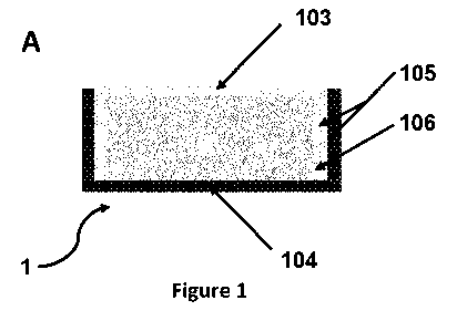
By way of illustration, and without being limited thereto, exemplary packaged
implantable
devices 1 are shown in FIG. 1 A ¨ F and FIG. 3. The packaged electronic device
according to the
invention comprises an electronic component 101 encapsulated by a hermetic
packaging
(whereby the hermetic packaging is defined by the layers surrounding and
encapsulating
electronic component 101), said packaging comprising at least top
encapsulation layer 103 and
a bottom encapsulation layer 104. The top and bottom encapsulation layers 103,
104 at least
CA 03113726 2021-03-22
9
WO 2020/115332
PCT/EP2019/084275
partially overlap so as to form areas of a double layer structure/s 105, 105',
e.g. at the side walls
of the encapsulated device. The top and bottom encapsulation layer are thus
typically designed
to not only (at least partially) cover the top surface and the bottom surface,
respectively, of the
electronic component to be packaged, but also extend beyond the top or the
bottom surface, e.g.
in vertical direction, thus also covering (at least partially) the side walls
of the device. For the
embodiments exemplified in FIG. 1 A to D, bottom encapsulation layer 104 forms
the outer layer
of the encapsulated device at the areas of double layer structure 105, 105'.
However, an assembly
100 with the top encapsulation layer 103 forming the outermost layer of the
device at such areas
of double layer structure 105, 105' is disclosed herewith as well.
The packaged electronic device 1 may generally be an electronic device of any
sort, including a
chip, stimulator, and a control or monitoring device. The electronic device is
preferably
implantable. The packaged electronic device is preferably useful for
biological or biomedical
applications, in particular for in vivo applications. Exemplary implantable
electronic devices
include retinal implants, including sub- and epiretinal implants, e.g. those
described in
W02016/180517 and PCT/EP2018/069159, or brain implants, e.g. for stimulating
the visual
cortex. Such implants allow to e.g. electrically stimulate neurons, e.g.
within a patient's eye or
brain (e.g. for regaining visual perception by stimulating the visual cortex
or by stimulating
neurons for treating Parkinson's disease), and/or to record electrical signals
of the patients
neurons. The hermetic packaging described herein ensures long term implant
half life without
the implanted electronic device being affected by the aqueous in vivo
environment at the
implantation site.
The electronic device 1 according to the present invention may include one or
more electronic
components 101, which is/are advantageously of cuboid shape and does/do
preferably not
comprise any electronic elements, e.g. a transistor, of three-dimensional
shape projecting
outwardly (projecting out of cuboid or the planes of the cuboid), to be
packaged, which may be
integrated circuits, also referred to as dies. Further types of such
components include micro
electromechanical systems (MEMS), including 0-th level packaged MEMS, thin-
film capped
MEMS, etc. The MEMs devices include for instance passive components,
actuators, sensors, etc.
Further examples of such components include micro-fluidics devices. Still
further examples
include batteries, such as a rechargeable battery, circuits, transistors,
resistors, photodiodes,
capacitors and the like. Electronic components 101 may actually represent a
stack of more than
one individual electronic units, for instance memory chips on integrated
circuits. Stacked units
forming an electronic component 101 may be encapsulated as whole such that
packaged
implantable electronic device 1 comprises electronic component 101 comprising
a stack of
electronic units.
CA 03113726 2021-03-22
WO 2020/115332 10
PCT/EP2019/084275
Electronic components 101 may ¨ in addition to the electronic units - also
comprise a (non-
encapsulating) layer 102. It may be positioned at the bottom surface of the
electronic component
101 (see FIG. 1 C and D), but alternatively also at its top surface. Layer 102
may comprise or
consist of any suitable substrate material including, for example, a
semiconductor material, e.g.
a silicon material, an electrically insulating material, a glass material, a
polymer material, and if
suitable an electrically conducting material such as for example a metal.
Preferably, layer 102
may comprise or consist of ceramics or glass, optionally selected from silicon
oxide or dioxide,
optionally obtained by oxidation of a silicon substrate. Layer 102 may
advantageously act as a
barrier protecting the electronic component 101 in the course of the packaging
method, in
particular at the step of removing substrate 110. For instance, layer 102 may
be composed of a
material that is not prone to decomposition/degradation when subjected to the
step of removal
of substrate 110. Electronic component 101, layer 102 and substrate 110 may
preferably be
selected to form a "silicon on insulator" or "SOI" wafer structure, which is
readily available and
widely used in the art. To this end, layer 102 may preferably be configured as
a layer of silicon
oxide disposed on a silicon substrate 110. Specifically for photodiodes or
other light sensitive
electronic components 101, the silicon dioxide layer 102 may preferably be
thermally grown on
electronic component 101 using known methods in the art, in order to provide
an interface
between electronic units/s and layer 102 of component 101 with favourable
electronic and/or
optical properties.
It is preferred that double layer structure 105, 105' resulting from top and
bottom encapsulation
layers 103, 104 at least partially, more preferably fully, covers side walls
106, 106' of electronic
component 101. The double-layered structure covering or at least partially
extending over side
walls 106, 106' advantageously confers an improved hermetic encapsulation and
may, in some
embodiments, preferably obviate the need for an additional encapsulation layer
surrounding top
and bottom encapsulation layer 103, 104, respectively. The double layer (105,
105') does
preferably not fully, but only partially cover the electronic component (101),
e.g. the double layer
(105, 105') covers the side walls (106, 106') of the electronic component
(101) only, but neither
the top side nor the bottom side of electronic component (101) are covered by
double layer (105,
105', 105a, 105b, 105c, 105d). Alternatively, the double layer (105, 105') may
cover the side
walls (106, 106') and the bottom side of the electronic component (101), but
not the top side
exposing photodiodes and/or electrodes (109). In another embodiment, only the
bottom side of
the electronic component (101) is covered by a double layer (105, 105', 105a,
105b, 105c,
105d).
CA 03113726 2021-03-22
WO 2020/115332
PCT/EP2019/084275
Top and/or bottom encapsulation layer/s 103, 104 are preferably capable of
providing a hermetic
seal for electronic component 101. The terms "hermetic seal" and "hermetically
sealing" and
"hermetic" are defined elsewhere herein. Top and/or bottom encapsulation layer
103, 104 may
be advantageously biocompatible. The term "bio-compatible" and "bio-
compatibility" refer to
the ability of a medical device to perform its intended function in the host
without eliciting any
undesired local or systemic effects for the host. Top and bottom encapsulation
layer 103, 104
may be corrosion-resistant. The term "corrosion resistant" refers to the
material's resistance
against its reaction with its aqueous environment as typically experienced
under in vivo
conditions. Redox-active compounds may corrode the device's material.
Corrosion of an implant
in vivo means that the implant is typically oxidized or otherwise chemically
attacked by its
environment. "Corrosion resistance" is the capacity to withstand deterioration
and chemical
modification/degradation, e.g. by redox reactions.
For embodiments (see e.g. embodiments of FIG. 1 A or of FIG. 1 B to D and of
FIG. 3 with an
additional coating of the top surface) characterized by an hermetic packaging
which is composed
of one single top and one single bottom encapsulation layer 103, 104 only
overlapping with each
other to preferably at least partially cover the electronic component's side
walls 106, 106', i.e.
the hermetic packaging does not comprise any further encapsulation layer, it
is preferred that top
and bottom encapsulation layer 103, 104 are both biocompatible and corrosion-
resistant, in
order to ensure both in vivo compatibility and proper function of the
electronic device 1. The
skilled person is readily able to select suitable materials for the top and
bottom encapsulation
layer 103, 104 preferably exhibiting bio-compatibility and/or corrosion-
resistance. Exemplary
suitable materials for the top and bottom encapsulation layer 103, 104 include
metals; ceramics
including oxides, nitrides, and carbides; diamond-like carbon; diamond; glass;
polymers, in
particular low permeability and/or dense polymers; and combinations thereof.
Specifically,
suitable metals may be selected from titanium (Ti), platinum (Pt), stainless
steel, titanium-nickel,
palladium, niobium, tantalum, and combinations or alloys thereof; suitable
ceramics may be
selected from silicon oxide, silicon nitride, silicon carbide, silicon
oxycarbide, titanium carbide,
titanium nitride, titanium oxide, aluminum oxide, aluminum nitride, zirconium
oxide, and
combinations thereof; suitable polymers may be selected from fluorocarbons,
polyurethane,
polyether ether ketone (PEEK), silicone, PDMS, parylene, polyimide,
polycarbonate,
polycarbonate urethane, silicone, silicone-polyester-urethane, durimide (photo-
definable
polyimide), cyclic olefin polymer (COP), cyclic olefin copolymer (COC),
polymethyl
methacrylate (PMMA), polyphenylene, polysulfone, polyphenylsulfone,
combinations thereof
and multi layers thereof. Top and bottom encapsulation layer 103, 104 may
comprise or consist
of the same or different materials. Top and bottom encapsulation layer 103,
104 may comprise
CA 03113726 2021-03-22
WO 2020/115332 12
PCT/EP2019/084275
or consist of monolayers or multilayers (e.g. more than one (sub)-layer) of
the materials specified
herein.
As indicated, hermetic packaging may comprise at least one additional top
encapsulation layer
103a, and/or an additional bottom encapsulation layer 104a (see e.g.
embodiments of Figures 1
E and 1 F), which preferably form at least one additional double layer
structure 105a, 105c at the
side walls and at least one additional double layer structure 105d at the
bottom (FIG. 1 E) or at
least two additional double layer structures (105a, 105b and 105c) at the side
walls (FIG. 1 F).
Such an additional double layer structure 105b, 105c may be due to the outer
encapsulation
layers 104 and 104a at the bottom side and/or the side walls of the device. In
particular, such an
additional bottom encapsulation layer 104a may cover at least partially, more
preferably fully,
side walls 106, 106' of electronic component 101. It may result ¨ as shown for
the embodiments
of FIG. 1 E and 1 F ¨ in a triple encapsulation layer side wall arrangement
with the top
encapsulation layer 103 forming an inner double layer structure 105 together
with bottom
encapsulation layer 104. The bottom encapsulation layer 104 furthermore forms
a second double
layer structure 105c together with the additional bottom encapsulation layer
104a resulting in a
triple layer structure at the side walls. Preferably, the at least one
additional double layer (105a,
105b, 105c) covers the side walls (106, 106') only, but neither the top side
nor the bottom side
of the electronic component (101). Analogous arrangements may be provided with
the bottom
layer encapsulation 104 being the innermost encapsulation layer at the side
wall areas such that
the top encapsulation layer 103 is sandwiched between the additional bottom
encapsulation
layer 104a as the outermost layer and the bottom encapsulation layer 104 being
in such an
embodiment the innermost encapsulation layer at the side wall areas. Moreover,
the additional
bottom encapsulation layer 104a may establish another double layer structure
105d at the bottom
side of the device with bottom encapsulation layer 104. FIG. 1 F exemplifies
the embodiment of
FIG. 1 E, however, additionally containing a partial additional top
encapsulation layer 103a on
top of encapsulation layer 103, thereby forming a double layer structure at a
peripheral region of
the top side of the packaged electronic device 1 according to the invention as
well. Three double
layer structures 105a, 105b and 105c (four side wall layers) are provided at
the side walls of
device 101. The use of more than one or more than 2 stacked encapsulation
layers may
advantageously improve hermetic encapsulation and provide an even more
reliable barrier
against external influences. Embodiments using such multilayer layer
configurations are still
compatible with undelayed wound healing and low local tissue irritation risk
upon implantation
surgery, as the additional layer does not prominently enlarge the implanted
device.
To this end, hermetic packaging may be provided with at least one additional
top encapsulation
layer 103a and/or at least one additional bottom encapsulation layer 104a.
Additional top
CA 03113726 2021-03-22
WO 2020/115332 13
PCT/EP2019/084275
encapsulation layer 103a is preferably applied onto encapsulation layer 103.
Additional bottom
encapsulation layer 104a is preferably applied onto bottom encapsulation layer
104. Thereby,
additional top and bottom encapsulation layer 103a, 104a preferably form the
outermost layers
of hermetic packaging and are thus in direct contact with the environment,
i.e. the body tissue,
when implanted. Top and bottom encapsulation layers 103, 104 are sandwiched
between the
outermost layers 103a, 104a and the top and bottom surface of electronic
component 101.
Therefore, top and bottom encapsulation layers 103, 104 may, but need not
necessarily, be
composed of a biocompatible material (in particular whenever they are not in
direct contact with
body tissue). However, top and bottom encapsulation layers 103, 104 preferably
comprise or
consist of a corrosion-resistant material as specified above in order to
protect electronic
component 101 against corrosive degradation by the environment. Additional top
and/or bottom
encapsulation layers 103a, 104a, if present, may, but need not necessarily be
composed of a
corrosion-resistant material (in particular, whenever layers 103, 104 are
suitable to protect
electronic component 101 against corrosion). Layers 103a and 104a, if present,
are preferably
composed of a biocompatible material.
Additional top and bottom encapsulation layers 103a, 104a may be composed of
monolayers or
multilayers (e.g. more than one (sub)-layer). Additional top and bottom
encapsulation layers
103a, 104a may be composed of the same or different materials.
For instance, preferred embodiments exhibiting "stacked" or multiple
encapsulation layers may
include a top and a bottom encapsulation layer 103, 104 made from a corrosion-
resistant
material, such as a metal, and may further be embedded in additional top
and/or bottom
encapsulation layers 103a, 104a made from a biocompatible material, e.g.
silicone, parylene,
hydrogels, etc.
(Additional) top and bottom encapsulation layers 103, 103a, 104 and 104a, in
particular in view
of their optional multi-layered structure, may also comprise at least one
conductive (sub)-layer
that permits electrical connection between the top and the bottom side or
portion of the packaged
device. It may be preferred that the circuitry is positioned on the top side.
One or several of those
(sub)-layers can be patterned, for instance in the shape of electrical tracks,
to permit one or more
electrical connections between the top and the bottom side of the packaged
device. For instance,
electronic component 101 may have circuitry on its top and/or bottom side that
are
interconnected by one of several layers of electrical tracks that are part of
at least one of the
encapsulation layers. Encapsulation layers 103, 103a, 104, 104a may therefore
comprise at least
one of patterned or non-patterned, electrically conductive or electrically
isolating (sub)-layers,
e.g. platinum, titanium, silicon carbide, silicon oxide, or silicon nitride.
In one embodiment, the
CA 03113726 2021-03-22
14
WO 2020/115332
PCT/EP2019/084275
conductive encapsulation (sub)-layers, such as metals, may all be electrically
connected to each
other and the electrical ground of the circuitry of the electronic component
101. In another
embodiment, the (patterned) passive conductive tracks or full conductive (sub)-
layers of at least
one of encapsulation layers 103, 103a, 104, 104a serve to establish an
electrical contact to the
circuitry.
The electronic device 1 according to the present invention may further include
at least one top
coating 107 as illustrated in FIG. 1 B ¨ D. Top coating 107 is preferably at
least partially
overlapped by top encapsulation layer 103 to advantageously ensure hermeticity
of the
packaging. As top coating 107 typically forms an outermost layer of the
hermetic packaging
according to the invention, e.g. at the top side of the inventive device, it
is in direct contact with
body tissue when implanted and thus preferably biocompatible. Preferably, top
coating 107 may
be corrosion-resistant as well. Top coating 107 may be composed of any
suitable material which
preferably adds a further functionality to the hermetic packaging of the
inventive device. E.g., in
particular for retinal implants as implantable electronic devices 1, top
coating 107 may be
composed of light transparent material. Advantageously, light (e.g. IR or
visible light) transparent
top coatings are useful for retinal stimulators, e.g., photovoltaic retinal
stimulators. Specifically,
top coating 107 may comprise or consist of a material selected from ceramic,
including SiC,
SiOC; 5i02; glass; diamond or diamond like carbon; aluminum oxides; titanium
oxides; and
combinations thereof. Top coating 107 may be composed of monolayers or
multilayers
(representing (sub)-layers) of the above-specified materials. Each (sub-)
layer may be composed
of identical or preferably distinct materials, in particular, as disclosed
above. The above-specified
materials of top coating 107 may be provided in amorphous or crystalline form,
or both.
As indicated, implantable electronic device 1 may preferably be an
electrically stimulating
device, such as a retinal implant or retinal stimulator. To this end, hermetic
packaging may, e.g.
by its top coating 107 and/or its top encapsulation layer 103, comprise
electronic traces 108
and/or cover, surround or embed electrodes 109 being part of and
electronically connected to
the electronic component 101. Preferably, electrodes 109 are provided within
or extending
beyond the hermetic packaging, in particular within or projecting beyond top
coating 107. Such
an embodiment is illustrated in FIG. 1 D. Top coating 107 may include holes or
feedthroughs to
pass or exchange electrical, light or chemical signals (e.g. for data
transmission) to and from
component 101. Such feedthroughs may for example include electrodes 109 to
transfer electrical
or ionic signals. Other exemplary feedthroughs that may be provided may be
liquid feedthroughs.
Feedthroughs may be connected to electrical leads for receiving or
transmitting electrical signals
(e.g. to sense signals or to electrically stimulate target cells or tissues).
Feedthroughs may be
CA 03113726 2021-03-22
WO 2020/115332
PCT/EP2019/084275
connected to flexible circuits connected to or in communication with further
electrodes or
devices remote from component 101.
Preferably, the electronic component 101 is an integrated circuit or a die,
with electrodes 109
being provided as feedthroughs. Electrodes 109 are preferably in electrical
communication with
5 electronic traces 108 disposed in or on said integrated circuit and may,
e.g., transduce electrical
signals generated through said integrated circuit. However, the skilled person
readily understands
that the provision of electronic traces 108 and/or electrodes 109 is not
restricted to electrical
stimulators, or retinal stimulators. Electronic traces may, for instance, also
be provided in devices
which are used as sensors or controllers or for other applications. In
implanted devices 1, selected
10 electronic traces 108 and/or electrodes 109 are preferably in direct
contact with the body tissue
when implanted. To this end, electrodes 109 may preferably be made of
biocompatible material.
Preferably, electronic traces 108 and/or electrodes 109 may be made of
corrosion-resistant
material to reduce or avoid corrosion and damage to electronic component 101.
Electronic traces
108 and/or electrodes 109 may preferably comprise or consist of a material
selected from
15 platinum, black/porous platinum, iridium, iridium/platinum, iridium oxide,
poly(3,4-
ethylenedioxythiophene) polystyrene sulfonate (PEDOT:PSS), PEDOT:PSS, (porous)
titanium
nitride, doped diamond or doped diamond like carbon, and graphene.
In some preferred embodiments, the inventive device 1 may be as illustrated by
FIG. 1 C or D,
comprising at least one electronic component 101, which preferably includes an
integrated
circuit or die and, optionally, includes further electronic units, such as
passives or active circuits,
fully packaged or embedded by a hermetic packaging comprising a top
encapsulation layer 103
and a bottom encapsulation layer 104, each composed of a metal, preferably
titanium. Electronic
components 101, 101' may include a layer 102, typically positioned at the
bottom side of the
electronic component, which may be composed of ceramics or glass, metal, or
combinations
thereof, preferably of silicon dioxide. In specific embodiments, layer 102 is
foreseen as a double
layer structure e.g. composed of one layer of ceramics or glass and one layer
of metal, or e.g. of
two metal layers. Electrodes 109 as part of component 101, 101' are preferably
made of platinum
(Pt), including porous and platinum black, (porous) TiN, iridium oxide, or
poly(3,4-
ethylenedioxythiophene) polystyrene sulfonate (PEDOT:PSS), establishing an
electrical
connection between electronic component 101 and the surrounding bodily fluid,
tissue or cells.
Electrodes 109, e.g. protruding upwardly such that they are embedded within
top layer 107 or
projecting beyond top layer 107, are preferably configured to establish an
electrical connection
between component 101, 101' and the surrounding environment, e.g. the body
tissue when
implanted. In preferred embodiments, electronic traces 108 may be provided as
part of the
electronic component 101, 101', e.g. on the top or upper surface of components
101, 101'.
CA 03113726 2021-03-22
WO 2020/115332 16
PCT/EP2019/084275
The hermetic packaging of the device 1 preferably comprises a top layer 107,
which is preferably
transparent. Top layer 107 may preferably be composed of a ceramic layer, more
preferably a
ceramic multilayer, even more preferably a ceramic multilayer comprising or
consisting of silicon
carbide, for instance amorphous silicon carbide. Top layer 107 may also
comprise electronic
traces, preferably from titanium (Ti), gold (Au), platinum (Pt), copper (Cu),
palladium (Pd) or
aluminum (Al) or a multi layer thereof,
Figure 3 shows another embodiment of an inventive packaged implantable device
1. The device
according to Figure 3 comprises the additional coating layer 107. The top
encapsulation layer
103 overlaps the coating layer 107 at its edge zone. Such a device 1 may e.g.
obtained by carrying
out the inventive method in combination with the steps of e.g. Figure 4 A
(step 300).
Preferably, device 1 may be a retinal implant packaged by the hermetic
packaging for
implantation in the eyes, preferably configured for being implanted epi- or
subretinally. It may
alternatively be configured for being implantable in the neural cortex, in
particular for contacting
neuronal cortex cells involved in visual data processing.
In a second aspect, the invention provides a system, comprising at least one
packaged
implantable device 1 as described herein, e.g. suitable or configured for
being implanted in the
eye. Device 1 may be obtainable by a method for manufacturing the claimed
device 1 as
disclosed herein. The system may also comprise other implantable or external
(non-implantable)
devices or components. The inventive system may also comprise more than one,
e.g. a plurality
of implantable devices 1. As indicated above, electronic components 101 to be
packaged may
include integrated circuits or dies, CMOS logics (such as steering,
programmable devices), MEMS
(such as membranes for example for pressure sensing, drug reservoirs,
microfluidics for drug
delivery), batteries, antenna (for example for loading a rechargeable battery,
for programming a
reprogrammable device).
The system may be provided together with external devices, such as video
glasses and an external
pocket processor in communication with component 101. Typically, component 101
may
communicate with external devices via wireless communication, e.g. through
infrared
communication, patterned light, RE communication, or any other suitable means.
Alternatively,
component 101 may communicate with external devices via wired connections,
e.g. including
intracutaneous wires. In preferred embodiments, the implantable component of
the system
according to the invention may comprise a hermetically packaged component 101
as described
herein as device 1 and as illustrated e.g. in Fig. 1 D as a retinal implant.
Packaged component
101 may preferably be implanted into the eye, more preferably being suitable
or configured for
implantation epi- or subretinally. Packaged electronic components 101, 101'
may be stacked
CA 03113726 2021-03-22
WO 2020/115332 17
PCT/EP2019/084275
and/or may be spaced apart from each other on a suitable support, or both.
Functionally distinct
packaged electronic components 101, 101' may be electrically connected via
electronic traces,
e.g. via metallization on a common support. The support may be flexible or
stretchable. Packaged
electronic components 101, 101' may be bonded to the support via suitable
bonding means. The
system may be provided with a global feedthrough, e.g. an electrical
feedthrough, a fluid
feedthrough etc.
In a third aspect, the present invention provides a method for producing or
manufacturing an
implantable packaged device 1, the method comprising (a) providing at least
one electronic
component 101 positioned on a substrate 110, (b) applying at least one top
encapsulation layer
103, 103a to electronic component 101, and (c) applying at least one bottom
encapsulation layer
104, 104a to electronic component 101, wherein the top and bottom
encapsulation layer 103,
103a, 104, 104a at least partially overlap so as to form a double layer
structure 105, 105', 105a,
105b, 105c, 105d, e.g. a double layer structure at/on the side wall areas of
device 1, at/on the
bottom side of device 1 and/or at/on the top side device 1. The double layer
(105, 105', 105a,
105b, 105c, 105d) does preferably not fully, but only partially cover the
electronic component
(101), e.g. the double layer (105, 105') covers the side walls (106, 106') of
the electronic
component (101), but neither the top side nor the bottom side of electronic
component (101) are
covered by double layer (105, 105', 105a, 105b, 105c, 105d). Alternatively,
the double layer
(105, 105') may cover the side walls (106, 106') and the bottom side of the
electronic component
(101), but not the top side exposing photodiodes and/or electrodes (109). In
another embodiment,
only the bottom side of the electronic component (101) is covered by a double
layer (105, 105',
105a, 105b, 105c, 105d).
In a fourth aspect, which may be an embodiment of the third aspect, the
present invention
provides a method (as e.g. illustrated in FIG. 2) for producing or
manufacturing an implantable
packaged device, said method comprising the following steps 309, 310, 311,
312, 313, 314,
315, optional step 316, and 317, preferably according to that order of steps.
In step 309, an assembly 100 is provided as a proto-structure with a
continuous layer 102 and a
continuous electronic component proto-structure 101 being positioned thereon.
At its bottom,
assembly 100 is supported by substrate 110.
In step 310, an assembly 100 of at least one, preferably a plurality of
electronic components 101
and 101' is provided, with said electronic components 101 and 101' being
spaced apart and
separated from each other on substrate 110 by a recess or gap. Adjacent
electronic components
101, 101' and substrate 110 define recesses 111. The recesses 111 are
laterally surrounded by
side walls 106, 106' of electronic components 101, 101'. In the present
example, the assembly
CA 03113726 2021-03-22
WO 2020/115332 18
PCT/EP2019/084275
may be an assembly of dies 101, 101' on a wafer 110. Advantageously, substrate
110 may
support a larger plurality of e.g. at least 10 or at least 20 or at least 50
or at least 100 or at least
500 components 101, 101'. The provision of assembly 100 according to step 310
includes
introduction of recesses 111 into at least one continuous electronic component
proto-structure
101 (as shown by step 309 of Figure 2) serving as the basic structure for the
electronic
components on which the inventive method is applied. It is composed of
suitable materials (as
described in the context of component 101 and layer 102), with potentially
several electronic
and/or optical features, such as electronic circuitry or photodiodes or other
sensor/stimulator
features, and being typically made of several patterned (sub)-layers, disposed
on/in substrate 110.
.. By step 310, electronic components 101, 101' are separated from each other
by introduction of
recesses 111 and thus singulated. Recesses 111 separating electronic
components 101, 101' are
introduced e.g. by dry or wet etching. That step of separating the electronic
components from
each another permits the manufacture of a larger number of electronic
components on the same
(typically flat) substrate 110 based on one single electronic component proto-
structure. This may
allow the inventive packaging method to be applied simultaneously to a
plurality of identical or
distinct (depending on the nature of the proto-structure) electronic
components 101, 101', which
enables a time- and cost-efficient manufacturing process.
In step 311, at least one top encapsulation layer 103 is applied to the top
surface of assembly
100, thereby coating the upper surface of electronic components 101, 101'
horizontally and
lining the walls of recesses 111 vertically. Suitable materials for top
encapsulation layer 103 are
described above. It will be understood that top encapsulation layers 103, 103a
may preferably
be composed of a conformal material, which is capable of conforming to the
contours of
electronic components 101, 101' and recesses 111 and thereby covers components
101, 101'
and the walls of recesses 111. Due to the preferred choice of conformal
materials and deposition
techniques, such as non-directional or partially directional physical vapor
deposition techniques,
sputtering, or chemical vapor deposition, for top encapsulation layer 103, a
reliable and
reproducible step-like (non-flat) coverage (including horizontal surface and
vertical side wall
coverage) is typically achieved. As indicated, step 311 may also comprise
adding monolayers or
multilayers of the same or different materials. Step 311 may also comprise
applying at least one
additional top encapsulation layer 103a (not shown in Figure 2, step 311) to
assembly 100,
typically after applying top encapsulation layer 103. At least one of the
(additional) top
encapsulation layers 103, 103a is preferably selected from a corrosion-
resistant material sufficient
to hermetically seal component 101 against the environment. The outermost top
encapsulation
layer 103 of the packaging, or, when adding an additional top encapsulation
layer, outermost
CA 03113726 2021-03-22
WO 2020/115332 19
PCT/EP2019/084275
encapsulation layer 103a is preferably composed of a biocompatible material in
order to reduce
or avoid irritation or damage of the surrounding body cells, tissues or
fluids.
In step 312, a removable layer 112 is applied to assembly 100, typically on
its upper surface, to
cover the previously coated components 101, 101' and lined recesses 111.
Preferably, removable
layer 112 may comprise or consist polymeric material preferably selected from
a resin, more
preferably a photosensitive resin (photoresist), and a dissolvable polymeric
material.
Photosensitive resins or photoresists (also known as photopolymers or light-
activated resins) are
oligorners or polymers that alter their properties when exposed to light,
typically in the ultraviolet
or visible region of the electromagnetic spectrum. Specifically, upon
irradiation of light,
photosensitive resins either polymerize into insoluble cross-linked network
polymers ("negative
photoresist") or decompose solid polymers into semi liquid or soluble or
dissolvable ("positive
photoresist"). In the context of the present invention, positive
photosensitive resins as commonly
known are used. Removable layer 112 is applied as a temporary protection of
components 101,
101' and, more specifically, top encapsulation layer 103, 103a for subsequent
processing.
Therefore, removable layer 112 is preferably composed of a material that can
be removed without
affecting electronic components 101, 101' or top encapsulation layer 103,
103a. Removing
removable layer 112 may preferably be accomplished by applying photoresist
developers or
photoresist strippers as commonly used in the semiconductor industry.
In step 313, removable layer 112 is removed from the assembly to expose top
encapsulation
layer 103 on the surface of components 101, 101'. The removing step may be
accomplished by
any suitable physical and/or chemical means, including grinding, dry or wet
etching and/or
stripping in wet solutions or in a plasma. Preferably, removing may preferably
leave a residual
amount of removable layer 112 in lined recesses typically covering the bottom
surface of the
recess. This residual amount of removable layer 112 is intended to form a
protective barrier or
"plug" protecting the top encapsulation layer lining recesses 111 against
degradation by
subsequent processing steps.
In particular in preferred embodiments with removable layer 112 being composed
of a positive
photoresist, step 313 may include sub-step 1) exposing assembly 100 to light
that is directed only
to the top surface (but not to the bottom portion of recesses 111) and sub-
step 2) applying a
photoresist developer to assembly 100. In this way, it is ensured that only
the photoresist
removable layer 112 at or near the top surface of assembly 100 is removed,
while a residual
amount of unexposed photoresist remains within the bottom portion of recesses
111.
Alternatively, removable layer 112 may be composed of a negative photoresist.
Under such
circumstances, step 313 may include sub-step 1) exposing assembly 100 to light
that is directed
CA 03113726 2021-03-22
WO 2020/115332 20
PCT/EP2019/084275
only to the bottom portion of recesses 111 (but not to the top surface) and
sub-step 2) applying a
photoresist developer to assembly 100. In this way, it is ensured that only
the unexposed
photoresist removable layer 112 at the top surface of assembly 100 is removed,
while a residual
amount of photoresist remains within the bottom portion of recesses 111.
In step 314 (as shown in FIG. 2, step 314a), assembly 100 is flipped (not
shown) and processed
upside down. The flipping of the device facilitates the processing of its
bottom side by making
the bottom side accessible from above. To this end, assembly 100 may be
temporarily attached
to temporary carrier 113. Temporary attachment may be accomplished by any
suitable adhesion
or bonding means, which are preferably reversible, e.g. via a suitable
adhesive. Preferably, the
adhesive may be characterized by an adjustable adhesive connection that can be
modified, e.g.
reduced by the application of e.g. heat, UV irradiation, laser light or other
light irradiation so as
to induce debonding of assembly 100 from temporary carrier 113. Temporary
carrier 113 may
be composed of any suitable solid material, e.g. silicon or glass.
This processing advantageously allows for the provision of stacked or double-
layered
encapsulation layer structures 105, 105', which ensures a hermetic sealing of
the electronic
component 101, 101' by the resulting packaging.
Step 314 includes several sub-steps of removing the layers from the bottom of
assembly 100 such
that lined recesses 111 are left open for being finally lined with bottom
encapsulation layer 104,
104' (see following step 315) to form a double layer structure 105, 105' at
least partially, more
.. preferably fully, covering the electronic components' side walls 106, 106'.
In step 314 a, substrate 110 is removed, thereby exposing the electronic
components' 101, 101'
bottom side, optionally covered by layer 102, and the top encapsulation layer
lining recesses
111. Step 314a may also be referred to as "thinning" of the substrate.
Substrate 110 may be
removed by any suitable physical and chemical means, including grinding and
etching.
.. Preferably, optional layer 102 may act as a barrier protecting the
components' 101, 101' bottom
side against thinning or from whatever other damage resulting from the removal
step, and may
thereby allow precise control of the removal of substrate 110 without
affecting electronic
components 101, 101'. The "thinning" is preferably performed until substrate
110 has been
removed (step 314b) or, more preferably until the residual amount of removable
layer 112 left
.. within recesses 111 is exposed by removal of layer 103, 103' (sub-step 314
c). In this way,
electronic components 101, 101' remain connected only by the top encapsulation
layer 103,
103' lining recesses 111 via removable layer 112.
CA 03113726 2021-03-22
WO 2020/115332 21
PCT/EP2019/084275
In sub-step 314 c, top encapsulation layer 103, 103' is removed, thereby
exposing residual
removable layer 112 forming a protective barrier within lined recesses. The
protective barrier
allows maintaining the integrity of top encapsulation layers 103, 103' for
subsequent processing,
in particular when removing of substrate 110. Advantageously, that approach
allows the
formation of a double-layer structure 105, 105' to be formed initially by
overlapping top
encapsulation layers 103, 103', and subsequently by applying bottom
encapsulation layers 104,
104' which preferably extend/s over and fully cover/s the entire side walls of
the resulting
electronic components 101, 101'. In this way, an improved and highly efficient
hermetic
encapsulation is enabled.
In sub-step 314d, residual removable layer 112 is removed, thereby exposing
lined recesses 111
for coating with bottom encapsulation layer 104, 104'. Preferably, removable
layer 112 may be
removed by exposing layer 112 to conditions or chemicals that are capable of
dissolving or
otherwise removing removable layer 112. Generally, removing may involve any
suitable physical
or chemical means, such as etching, stripping, or other treatment with
suitable chemicals or
solvents capable of removing removable layer 112. In case of a photoresist
removable layer 112,
removing may preferably comprise: applying light and a photoresist developer,
applying a
photoresist developer alone or photoresist stripping in wet solutions or a
plasma.
Selection of suitable techniques for removing the individual layers during
processing is well
known. The choice of the appropriate techniques will usually depend on the
layer's material to
be removed. It will be understood that appropriate removing techniques are
typically selected
based on the nature of the material to be removed, i.e. each layer is removed
by a technique
which preferentially or exclusively removes the target layer only rather that
other, non-target
layers or materials of assembly 100.
In step 315, at least one bottom encapsulation layer 104, 104a is applied to
assembly 100,
preferably in upside-down orientation for processing from above, to coat ¨ at
the bottom side -
electronic components 101, 101' and recesses 111 lined with top encapsulation
layer 103, 103a.
Suitable materials for bottom encapsulation layer 104, 104a are described
above. It will be
understood that bottom encapsulation layers 104, 104a may preferably be
composed of a
conformal material or deposited by techniques that are at least partially
directional, which is
capable of conforming to the contours of electronic components 101, 101' and
recesses 111 and
thereby covers components 101, 101' and the inner walls of recesses 111
previously lined with
top encapsulation layer 103, 103a. Due to the preferred choice of conformal
materials and
deposition techniques for bottom encapsulation layer 104, 104a, a highly
satisfying step-like
coverage is typically established. As indicated, step 315 may allow applying a
monolayer or
CA 03113726 2021-03-22
WO 2020/115332 22
PCT/EP2019/084275
multilayers of the same or different materials. Step 315 may also comprise ¨
in addition to
applying bottom encapsulation layer 104 ¨ a further sub-step of applying at
least one additional
bottom encapsulation layer 104a (not shown in step 315) to assembly 100,
typically after
applying bottom encapsulation layer 104. At least one bottom encapsulation
layer 104, 104a is
preferably selected from a corrosion-resistant material allowing to
hermetically seal components
101, 101' against the environment. The outermost bottom encapsulation layer
104, 104a being
the interface to the environment is preferably composed of a biocompatible
material in order to
reduce or avoid irritation of or affecting the surrounding body cells, tissues
or fluids. As indicated,
step 315 may comprise adding monolayers or multi layers of the same or
different materials.
The inventive method enables top and bottom encapsulation layer/s 103, 103a,
104, 104a to be
preferably applied so as to at least partially overlap and form a double layer
structure 105, 105',
105a. Said double layer structure 105, 105a preferably at least partially,
more preferably fully,
covers the electronic components' side walls 106, 106'; in particular, by
using removable layer
112 as a protective barrier for top encapsulation layer/s 103, 103a lining
recesses 111 (see step
314), and by preferably altering the orientation of the assembly 100
("flipping") upside-down
(allowing upside-down processing of assembly 100) before applying bottom
encapsulation layer
104, 104a.
One or more of top and/or bottom encapsulation layers 103, 103a, 104, 104a (or
at least a portion
thereof) may be patterned using for instance photolithography and etching or
lift-off during the
process, to introduce e.g. continuous tracks (e.g. at least at the sidewall
area) allowing electrical
interconnects between the top and bottom side of electronic components 101,
101'.
By optional step 316, assembly 100 is secured or fastened to supporting layer
114, while
assembly 100 as provided according to step 315 is released from temporary
carrier 113,
preferably subsequently. Securing or bonding may be accomplished by any
suitable bonding
means, e.g. via a suitable adhesive. The adhesive may preferably be
characterized by an
adjustable adhesive connection or bonding, which may be modified and, in
particular, reduced
by applying heat and/or UV light and/or laser light. Supporting layer 114 may
preferably be
composed of a flexible material, e.g. a thin film, which enables transport or
storage of the
electronic components 101, 101'. Exemplary materials include flexible
polymers, such as so-
called semiconductor õdicing tapes". Advantageously, the use of a flexible
film allows removing
the electronic components 101, 101', such as dies, by a õdie picking" process,
whereby the die
is pushed from the back using one or multiple pins, and by using a vacuum
"pick-up tool" to lift
or take off the die from the front. That step is typically carried out by
automatic õdie picking"
machines.
CA 03113726 2021-03-22
WO 2020/115332 23
PCT/EP2019/084275
That release from supporting layer 114 is shown in step 317. The resulting
device 1 is
encapsulated by top and bottom encapsulating layers 103 and 104 resulting from
step 315. Or it
is released upon step 316 from its supporting layer 114. The assembly 100
according to step 317
represents an embodiment of the invention being tightly encapsulated and
having the desired
hermeticity for its in vivo implantation. It is characterized by a double
layer structure 105, 105'
formed by encapsulation layers 103 and 104 over the entire side wall as a
result of the inventive
method as shown by the embodiment of FIG. 2.
The inventive method may optionally further comprise step 317 for providing a
top coating 107.
Top coating 107 may either be applied prior to applying top encapsulation
layer/s 103, 103a in
step 311. Or, alternatively, top coating 107 may be applied only after
applying the top
encapsulation layer 103, 103a in step 311, e.g. either prior to step 312 or
after step 316. Should
the coating step 400 be carried out prior to step 311, it is carried out
before the recesses 111 are
introduced into assembly 100 as described above (i.e. onto the assembly 100 of
step 309 prior
to step 310 of FIG. 2) or after the recess has been introduced (applied onto
the assembly 100 of
step 310 prior to step 311). Depending on when the top coating 107 is applied
to assembly 100
in the course of the inventive method, the top encapsulation layer/s 103, 103a
may at least
partially overlap the coating layer 107 or, alternatively, coating layer 107
may at least partially
overlap with encapsulation layers 103, 103a. When applying top coating 107 by
step 400 only
after step 316, it preferably forms a further layer on top of the layers 103,
103a forming the
outermost upper layer of the resulting device 1 being in direct contact with
the environment.
Top coating 107 is ¨ according to one embodiment - preferably applied to the
electronic
components 101, 101' (or assembly's 100 top side) prior to the application of
encapsulation
layer(s) 103, 103a. The application may involve any suitable means, preferably
deposition,
including chemical vapor deposition (CVD), including plasma-enhanced CVD
(PECVD), or
physical vapor deposition (PVD), or atomic layer deposition (ALD) or
underlying layer oxidation.
Subsequently, top coating 107 is preferably partially removed, followed by
application of at least
one top encapsulation layer/s 103, 103a such that top coating 107 and
encapsulation layer(s)
103, 103a preferably at least partially overlap with each other. It may be
preferred to allow the
at least one top encapsulation layer/s 103, 103a to overlap the coating layer
107 at least at the
edge region of the coating layer 107. Partial removal of top coating 107 is
preferably envisaged
for exposing the assembly's edges. Removal involves any suitable means, e.g.
any chemical or
physical process, preferably wet or dry etching and/or lift-off. Partial
overlap of top coating 107
and top encapsulation layer/s 103, 103a due to the resulting packaging
hermetically encloses
electronic components 101, 101' without interfering with the intended function
of top coating
107.
CA 03113726 2021-03-22
WO 2020/115332 24
PCT/EP2019/084275
Alternatively, top coating 107 may be applied only after applying top
encapsulation layer/s 103,
103a in step 311. To this end, at least one top encapsulation layer/s 103,
103a is applied to the
electronic components' 101, 101' from above at their top side. Subsequently,
top encapsulation
layer/s 103, 103a is partially removed from electronic component 101, 101' for
top coating 107
to be applied, e.g. at the site of removed portion of the top encapsulation
layer 103, 103a. E.g.,
top encapsulation layer/s 103, 103a may be removed from the central portion of
the surface of
electronic components 101, 101', while the peripheral portion covering the
edges of the
electronic components 101, 101' remains covered by the at least one top
encapsulation layer/s
103, 103a. Any suitable means may be applied, e.g. any chemical or physical
process, preferably
wet or dry etching and/or lift-off. Thereafter, top coating 107 is applied to
electronic components
101, 101', such that top coating 107 and encapsulation layer/s 103, 103a
preferably at least
partially overlap with each other. As above, top coating 107 may be preferably
applied by
deposition, including chemical vapor deposition (CVD), including PECVD, or
physical vapor
deposition (PVD), or atomic layer deposition (ALD) or underlying layer
oxidation.
The resulting embodiments exhibiting top coating 107 depend on the specific
underlying method
applied and the stage of the carrying out step 400 in the course of the
inventive method. Such
alternatives of applying top coating 107 are illustrated in FIG. 4 A-C.
All of the embodiments shown in Figure 4 A-C represent alternative preferred
embodiments of
step 400 at distinct stages of the inventive method. By step 400 of Figure 4
A, the components
101, 101' being separated by recess 111 (see step 310 of the method according
to FIG. 2) are
coated (coating layer 107) at their upper surface and along the inner vertical
surface walls of the
recess 111 (or rather side walls 106, 106' of the electronic components 101,
101' forming recess
111). The coating layer 107 is patterned by etching or liftoff. When using the
etching process,
the material 107 is deposited first; then, the photoresist is applied and
patterned and the material
107 is etched from the regions not covered by photoresist. Finally, the
photoresist is removed.
When lift-off is used, the patterning of the photoresist is done before
deposition of the material
107; after depositing material 107, the resist and the material 107 over the
photoresist is removed
to leave layer 107 where the photoresist had previously been removed before
depositing material
107.
The embodiment according to step 400 of Figure 4 B is, however, distinct from
Figure 4 A in that
the coating by coating layer 107 is applied prior to introducing recess 111
(separating electronic
components 101, 101' from each other). The patterning or lift-off process is
applied such that
recess 111 is only introduced after the patterning or lift-off step 400
according to FIG. 4 B. Both
embodiments of FIG. 4A and 4 B thereafter continue by step 311 (of Figure 2)
applying the top
CA 03113726 2021-03-22
WO 2020/115332 25
PCT/EP2019/084275
encapsulating layer 103 to the exposed upper surface and thereby also lining
recess 111. Step
400 according to FIG. 4 C is distinct from step 400 of the embodiments of
Figures 4 A and 4 B
by an altered order of steps. For the embodiment of Figure 4 C steps 310 and
311 (of FIG. 2) are
performed first and only after step 311 (applying the top encapsulation layer
103) the electronic
components 101, 101' are coated by coating layer 107. Thus, the embodiment of
step 400
according to Figure 4 Gallows the coating layer 107 to (partially) overlap the
top encapsulating
layer 103, in contrast to the embodiments of Figures 4 A and 4 B.
It is common to all of these embodiments of step 400 that they may involve
etching or lift-off.
In the etching process of step 400, top coating 107 is applied to the surface
of components 101,
101'. Subsequently, a photoresist layer is applied using suitable methods,
e.g. spin coating, which
is optionally baked by applying heat. Thereafter, a mask is applied which
defines the desired
patterning of the resulting top coating 107, and allows exposing the "masked"
photoresist to light.
Subsequently, a suitable developer is added which removes the photoresist. In
case of positive
photoresists, the light-exposed parts are removed. In case of negative
photoresists, the non-light
exposed parts of the resist are removed. After the "developing step" optional
curing or hardening
of the resist may be performed by applying heat. Wet or dry etching may follow
to selectively
remove the parts of top coating 107 which are not covered by the photoresist,
while the
photoresist-covered parts of top coating 107 are retained. Finally, the
remaining resist is removed
by stripping in a suitable stripping solution or plasma to yield a top coating
107 which is patterned
as defined by the mask.
In the alternative lift-off process for step 400, photoresist is applied onto
the top surface of
component 101, 101', or onto any other layer which is supposed to support top
coating 107, e.g.
by spin coating. Optionally, it is baked by applying heat. Subsequently, a
mask which defines
the desired patterning of the resulting top coating 107 is applied to the
photoresist, and the
"masked" photoresist is exposed to light. Thereafter, a suitable developer is
applied which
removes the photoresist. In case of positive photoresists, the light-exposed
parts are removed. In
case of negative photoresists, the non-light exposed parts of the resist are
removed. The
"developing step" is followed by optionally curing or hardening the resist by
applying heat. Top
encapsulation layer 103 (or any other layer which is supposed to partially
cover top coating 107)
is deposited on the photoresist. Finally, a suitable stripping solution is
applied, optionally together
with the application of ultra-sound, to lift-off the patterned photoresist
together with the covering
layer, and to retain the covering layer only where the underlying photoresist
was previously
removed.
CA 03113726 2021-03-22
WO 2020/115332 26
PCT/EP2019/084275
Each of the resulting assemblies 100 shown in Figures 4 A to 4 C may be
further processed
according to the inventive method, e.g. by continuing the production process
by its step 312 (see
Figure 2).
Furthermore, the inventive method may include an optional step 500 of
providing e.g. electronic
traces 108, photodiodes and/or electrodes 109 within the hermetic packaging,
e.g. at the top or
at the bottom of electronic component 101, 101'. That optional step 500 is
typically carried when
the upper surface of electronic component 101 is exposed and accessible to
further modification,
e.g. at step 309 or 310. Alternatively, it may be carried out after the outer
layers have been
applied, e.g. at step 316 or thereafter. That alternative approach is enabled
by removing
previously applied layer/s or coatings, at least regionwise. Thus, step 500
modifies electronic
component 101. Thereby, electronic traces 108 and/or electrodes 109 may be
applied to the
surface of electronic components 101, 101', typically underneath top coating
107 and top
encapsulation layer/s 103, 103a, by any suitable deposition technique,
including chemical vapor
deposition (CVD), physical vapor deposition, such as e-beam evaporation or
(reactive) sputtering,
electrochemical deposition and electrodeposition or patterning, including lift-
off or etching, as
described in more detail below.
Modification of the electronic component 101 by vertically or upward
protruding structures (e.g.
electrodes, see e.g. FIG. 1 D) may have an impact on the nature of the top
encapsulating layer/s
103, 103a and/or coating layer/s 107. They may e.g. exhibit holes interrupting
one or more of
these layer/s. Preferably, electrodes 109 may e.g. be provided within or
extending beyond top
coating 107 and/or, additionally or alternatively, within or beyond top
encapsulation layer/s
103/103a.
Electrodes 109 may also be introduced only after the provision of the hermetic
packaging has
been established by locally removing top coating 107 and/or top encapsulation
layer/s 103, 103a
so that the surface of components 101, 101' is typically completely exposed at
the electrode
deposition sites. The electrodes 109 on the surface of components 101, 101'
may be added, e.g.
by depositing a metal or other electrode material layer. First, top coating
107 and/or top
encapsulation layer/s 103/103a may be partially removed to generate holes or
feedthroughs for
forming electrodes 109. Removing may be accomplished by any suitable
technique, e.g. by
etching. Subsequently, electrode material is applied to top coating 107 and/
or top encapsulation
layer/s 103/103a. The excess electrode material is, e.g. subsequently,
removed, for instance by
etching or lift-off, such that the electrode material is preferably
exclusively retained at the sites of
the holes or feedthroughs of top coating 107 and/or top encapsulation layer/s
103/103a, and,
optionally, partially overlaps with top coating 107 and/or top encapsulation
layer/s 103/103a.
CA 03113726 2021-03-22
WO 2020/115332 27
PCT/EP2019/084275
Such an embodiment may be envisaged, whenever electrodes 109 shall be larger
in diameter
than the hole or feedthrough size.
Alternatively, electrodes 109 may be formed by electronic traces 108
underneath top coating
107 and/or top encapsulation layer/s 103/103a. To this end, top coating 107
and/or top
encapsulation layer/s 103/103a is/are partially removed, e.g. by etching or
lift-off, to form holes
or feedthroughs exposing portions of the underlying electronic traces 108.
The foregoing description details certain embodiments of the invention. It
will be appreciated,
however, that no matter how detailed the foregoing appears in text, the
invention may be
practiced in many ways. It should be noted that the use of particular
terminology when describing
certain features or aspects of the invention should not be taken to imply that
the terminology is
being re-defined herein to be restricted to including any specific
characteristics of the features or
aspects of the invention with which that terminology is associated.
While the above detailed description has shown, described, and pointed out
novel features of
the invention as applied to various embodiments, it will be understood that
various omissions,
substitutions, and changes in the form and details of the device or process
illustrated may be
made by those skilled in the technology without departing from the spirit of
the invention. The
scope of the invention is indicated by the appended claims rather than by the
foregoing
description. All changes which come within the meaning and range of
equivalency of the claims
are to be embraced within their scope.
CA 03113726 2021-03-22
WO 2020/115332 28 PCT/EP2019/084275
ITEMS
1. An implantable device comprising an electronic component (101)
encapsulated by a
hermetic packaging (10), said packaging comprising a top encapsulation layer
(103) and
a bottom encapsulation layer (104), wherein top and bottom encapsulation layer
(103,
104) at least partially overlap so as to form a double layer (105, 105').
2. Implantable device according to item 1, wherein the double layer (105,
105') at least
partially, more preferably fully covers the side walls (106, 106') of
electronic component
(101).
3. Implantable device according to item 1 or 2, wherein the double layer
(105, 105') does
not fully, but only partially cover the electronic component (101).
4. Implantable device according to any one of items 1 to 3, wherein the
double layer (105,
105') covers the side walls (106, 106') of the electronic component (101)
only, but neither
the top side nor the bottom side of electronic component (101).
5. Implantable device according to any one of items 1 to 4, wherein top
and/or the bottom
encapsulation layer (103, 104) is/are biocompatible.
6. Implantable device according to any one of items 1 to 5, wherein top
and/or bottom
encapsulation layer (103, 104) is/are corrosion-resistant.
7. Implantable device according to item 5 or 6, wherein top and/or bottom
encapsulation
layer (103, 104) comprise or consist of metal; ceramic including oxides,
nitrides, and
carbides, preferably metal oxides, metal nitrides and metal carbides; diamond-
like
carbon; diamond; glass; polymers; combinations thereof, or combinations or
multi layers
thereof.
8. Implantable device according to item 7, wherein said metal is selected
from Ti, Pt,
stainless steel, titanium-nickel, palladium, niobium, tantalum, combinations
or alloys
thereof, and multilayers thereof; wherein said ceramic is selected from the
group
consisting of silicon oxide, silicon nitride, silicon carbide, silicon
oxicarbide, titanium
carbide, titanium oxide, aluminum oxide, aluminum nitride, zirconium oxide,
combinations thereof, and multilayers thereof; and/or said polymer is selected
from the
group consisting of fluorocarbons, polyurethane, polyether ether ketone
(PEEK), silicone,
CA 03113726 2021-03-22
WO 2020/115332 29
PCT/EP2019/084275
PDMS, parylene, polyimide, polycarbonate, polycarbonate urethane, silicone,
silicone-
polyester-urethane, durimide (photo-definable polyimide), cyclic olefin
polymer (COP),
cyclic olefin copolymer (COC), polymethyl methacrylate (PMMA), polyphenylene,
polysulfone, polyphenylsulfone, combinations thereof and multilayers thereof.
9. Implantable device according to any one of the preceding items, wherein
the packaging
further comprises at least one top coating (107), preferably wherein top
coating (107) and
the top encapsulation layer (103) at least partially or fully overlap with
each other.
10. Implantable device according to item 9, wherein top coating (107) is
biocompatible.
11. Implantable device according to item 9 or 10, wherein top coating (107)
is corrosion
resistant.
12. Implantable device according to any one of items 9 to 10, wherein top
coating (107) is
transparent.
13. Implantable device according to any one of items 9 to 12, wherein top
coating (107)
comprises or consists of a material selected from the group consisting of
ceramic; glass
including SiC, SiOC; SiO2; diamond or diamond like carbon; aluminum oxides;
titanium
oxides; combinations thereof; and multi layers thereof.
14. Implantable device according to any one of items 9 to 13, wherein said
device, preferably
said top coating (107) further comprises electronic traces (108)
electronically connected
to the electronic component (101), said electronic traces (108) preferably
forming
electrodes within or protruding from top coating (107).
15. Implantable device according to item 14, wherein said electronic traces
form electrodes,
which are preferably bio-compatible and corrosion-resistant.
16. Implantable device according to item 14 or 15, wherein said electronic
traces comprise
or consist of a material selected from the group consisting of platinum,
black/porous
platinum, iridium, iridium/platinum, iridium oxide, PEDOT:PSS, titanium
nitride, doped
diamond or doped diamond like carbon and graphene, and combinations thereof.
17. Implantable device according to any one of the preceding items, wherein
said electronic
component (101) encapsulated by said hermetic packaging (10) comprises a layer
(102).
18. Implantable device according to item 17, wherein layer (102) comprises
or consists of
ceramics or glass, optionally selected from silicon oxide, optionally obtained
by oxidation
of a silicon substrate.
CA 03113726 2021-03-22
WO 2020/115332 30 PCT/EP2019/084275
19. Implantable device according to any one of the preceding items, further
comprising at
least one additional top encapsulation layer (103a) on top of top
encapsulation layer (103)
and/or at least one additional bottom encapsulation (104a) encapsulating
bottom
encapsulation layer (104).
20. Implantable device according to item 19, wherein further encapsulation
layers (103a,
104a) overlap so as to form at least one additional double layer (105a, 105b,
105c)
optionally covering at least partially, more preferably fully, side walls
(106, 106') of
electronic component (101).
21. Implantable device according to item 20, wherein the at least one
additional double layer
(105a, 105b, 105c) covers the side walls (106, 106') only, but neither the top
side nor the
bottom side of the electronic component (101).
22. Implantable device according to any one of items 19 or 21, wherein top
and/or bottom
encapsulation layer (103, 103', 104, 104') is/are corrosion resistant and
optionally bio-
compatible.
23. Implantable device according to any one of items 19 to 22, wherein the
at least one
additional top and/or bottom encapsulation layer(s) (103a, 104a) is/are
biocompatible
and optionally corrosion-resistant.
24. Implantable device according to any one of the preceding items, wherein
top and/or
bottom encapsulation layers (103, 104) and/or optionally further top and/or
bottom
encapsulation layers (103a, 104a) comprise or consist of the same or a
different material.
25. Implantable device according to any one of the preceding items, wherein
the implantable
device comprises photodiodes and/or electrodes (109) being exposed to the
environment,
preferably embedded by a top coating layer and/or a top encapsulation layer
such that
their outer top surface is exposed to the environment.
26. Implantable device according to any one of the preceding items, wherein
the implantable
device is configured for being implantable in the eye, preferably as a retinal
implant being
configured for being implantable epi- or subretinally.
27. An implantable system comprising at least one packaged device according
to any of items
1 to 26.
CA 03113726 2021-03-22
WO 2020/115332 31
PCT/EP2019/084275
28. A method for packaging an implantable device, the method comprising
(a) providing at least one electronic component (101) on a substrate (110);
(b) applying at least one top encapsulation layer (103, 103') to electronic
component (101, 101'); and
(c) applying at least one bottom encapsulation layer (104, 104') to electronic
component (101, 101');
wherein the top and bottom encapsulation layer (103, 103', 104, 104') at least
partially
overlap so as to form a double layer (105, 105', 105a, 105b, 105c).
29. A method for packaging an implantable device, said method comprising
the steps of:
(i) providing an assembly (100) of at least one, preferably a plurality of
electronic
components (101, 101') spaced apart from each other on a substrate (110),
wherein
adjacent electronic components (101, 101') and substrate (110) define recess
(111)
in between electronic components (101, 101');
(ii) applying at least one top encapsulation layer (103, 103') to assembly
(100),
thereby coating electronic components (101, 101') and lining recess (111);
(iii) applying a removable layer (112) to assembly (100);
(iv) partially removing removable layer (112), thereby leaving a residual
amount of
removable layer (112) within lined recess (111);
(v) preferably upending or flipping assembly (100) upside down;
(vi) removing (a) substrate (110), (b) top encapsulation layer (103) and (c)
residual
amount of removable layer (112) from the assembly's bottom side; and
(vii) applying at least one bottom encapsulation layer (104, 104') to assembly
(100),
thereby preferably coating electronic components (101, 101') and recess (111),
wherein the top and second bottom encapsulation layer (103, 103', 104, 104')
are applied
so as to at least partially overlap and forming a double layer (105, 105').
30. The method according to item 28 or 29, wherein the double layer (105,
105') is provided
so as to at least partially, more preferably fully cover the electronic
component's side
walls (106, 106').
CA 03113726 2021-03-22
WO 2020/115332 32 PCT/EP2019/084275
31. The method according to any one of items 28 to 30, wherein the double
layer (105, 105')
covers the side walls (106, 106') only, but neither the top side nor the
bottom side of the
electronic component (101).
32. The method according to any one of items 28 to 31, further comprising a
step of providing
a top coating (107) by
(a) applying a top coating (107), preferably as defined in any one of the
preceding items,
to the top side of electronic component (101, 101') (b) partially removing top
coating
(107) (c) applying at least one top encapsulation layer (103, 103'),
preferably as defined
in any one of the preceding items, to the electronic component (101, 101'),
such that top
coating (107) and encapsulation layer(s) (103, 103') preferably at least
partially overlap
with each other;
or
(a') applying at least one top encapsulation layer(s) (103, 103'), preferably
as defined in
any one of the preceding items, to electronic component (101, 101'), (b')
partially
removing top encapsulation layer(s) (103, 103') from electronic component
(101, 101'),
(c') applying a top coating (107), preferably as defined in any one of the
preceding items,
to electronic component (101, 101'), such that top coating (107) and
encapsulation
layer(s) (103, 103') preferably at least partially overlap with each other.
33. The method according to item 32, wherein step (2) includes partially
removing top
coating (107) or top encapsulation layer(s) (103, 103') by any chemical or
physical
process, preferably wet or dry etching and/or lift-off.
34. The method according to item 32 or 33, wherein top coating (107) is
applied by
deposition, including chemical vapor deposition (CVD), including PECVD, or
physical
vapor deposition (PVD), or atomic layer deposition (ALD) or underlying layer
oxidation.
35. The method according to any one of items 28 to 34, further comprising a
step of providing
electronic traces (108) and/or electrodes (109), preferably within top coating
(107), by
deposition, including physical vapor deposition or electrodeposition, and/or
patterning,
including lift-off or etching.
36. The method according to any one of items 29 to 35, further comprising
prior to step (iv)
a step of attaching the assembly's top side to a temporary carrier (113).
CA 03113726 2021-03-22
33
WO 2020/115332 PCT/EP2019/084275
37. The method according to any one of items 29 to 35, wherein the
substrate (110), top
encapsulation layer (103) and/or removable layer (112) are removed by means
each
independently selected from physical and chemical means, including grinding,
etching
and/or stripping.
38. The method according to any one of items 28 to 37, wherein top and/or
bottom
encapsulation layer (103, 104) are biocompatible.
39. The method according to any one of items 28 to 38, wherein top and/or
bottom
encapsulation layer (103, 103a, 104, 104a) are corrosion-resistant.
40. The method according to any one of items 28 to 39, wherein top and/or
the bottom
encapsulation layer (103, 103a, 104, 104a) comprise or consist of a material
optionally
selected from a metal, including titanium, platinum, stainless steel, titanium-
nickel,
palladium, niobium, tantalum, alloys and multilayers thereof; a ceramic,
including metal
oxides, metal nitrides, and metal carbides such as silicon oxide, silicon
nitride, silicon
carbide, silicon oxicarbide, titanium carbide, aluminum oxide, aluminum
nitride,
zirconium oxide and multilayers thereof; diamond-like carbon; diamond; glass;
low
permeability and/or dense(specification!) polymers, including fluorocarbons,
polyurethane, PEEK, silicone, PDMS, parylene, polyimide; or multilayers
thereof.
41. The method according to any one of items 30 to 40, wherein removable
layer (112)
comprises or consists of a material selected from a polymeric material,
preferably a resin,
more preferably a photosensitive resin, and a dissolvable polymeric material.
42. The method according to any one of items 32 to 41, wherein top coating
(107) is
biocompatible.
43. The method according to any one of items 32 to 42, wherein top coating
(107) is
corrosion-resistant.
44. The method according to any one of items 32 to 43, wherein top coating
(107) is
transparent.
45. The method according to any one of items 32 to 44, wherein top coating
(107) comprises
or consists of a material selected from ceramics; glass, including PECVD SiC,
SiOC; S102;
diamond or diamond like carbon; aluminum oxides; titanium oxides; or
multilayers
thereof.
CA 03113726 2021-03-22
34
WO 2020/115332
PCT/EP2019/084275
46. The method according to any one of items 28 to 45, wherein the method
provides a
packaged device according to any of item 1 to 26.