Note : Les descriptions sont présentées dans la langue officielle dans laquelle elles ont été soumises.
CA 03117005 2021-04-19
WO 2020/081807 PCT/US2019/056729
BI-DIRECTIONAL COUPLER WITH TERMINATION POINT
FOR A TEST POINT
BACKGROUND
100011 A test point may be used to measure the performance of an upstream or
downstream
connection in a network. In one implementation, two separate directional
couplers are used to
connect two test points (TPs) to measure an upstream and a downstream signal.
One directional
coupler for a first test point is used for the downstream direction and a
second directional coupler
for a second test point is used for the upstream connection. This leaves an
isolating port that is
terminated by a termination load, such as a 75-ohm termination load if the
test point also has a
load of 75-ohms. The coupler directivity is limited by how good the isolating
port is terminated
and this achieves maximum directivity performance because the load of the
isolating port is the
same as the load of the test point.
0002] In a full duplex node design, the use of two separate couplers may add
too much of a loss
at an output of a power amplifier connected to the coupler. With use of two
separate couplers, the
insertion loss will be doubled, from 1 dB in single coupler case to 2 dB in
two coupler case. The
output RF amplifier may already be running very close to its clipping point.
With the use of a
single coupler, the RF amplifier will not need to provide as much
amplification compared to the
two coupler case, which will improve the system level modulation error ration
or bit error ratio
(MER/BER) performance. Accordingly, a single bi-directional coupler may have
to be used for
both the upstream direction and the downstream direction. One advantage of
using a bi-directional
coupler is there is a lower insertion loss in the connection because only one
coupler is used in both
the upstream and the downstream directions. However, isolation between the
upstream connection
and the downstream connection may be an issue. The directivity of a coupler is
defined as the
power difference at any given coupling port when the same amount of power is
injected into either
the downstream direction or the upstream direction. A coupler may have around
25-30 decibels
(dB) directivity, which means there may be 25-30dB isolation between the
upstream direction and
the downstream direction at any given coupling port. However, this is based on
an ideal 75-ohm
1
CA 03117005 2021-04-19
WO 2020/081807 PCT/US2019/056729
termination at the isolating port. In a bi-directional coupler, the
termination at the isolating port is
typically not the perfect 75-ohm termination and thus will limit the isolation
between the
downstream and the upstream to the return loss of the isolating port. For
example, the ideal
isolation may not be achieved because one or both of the upstream test point
and the downstream
test point may not be connected to the bi-directional coupler. For example, a
user may only be
using one of the test points to test network traffic in one direction. This
leaves an open test point
port. In the full duplex node design, a 20dB test point is required and a 10dB
coupler is used. The
best return loss from the open test point port is 20dB, which would limit the
coupler directivity at
20dB even when the coupler has 30dB directivity by design when all ports are
properly terminated.
In the worst case, when two reflections are added in phase from two open test
point ports, the total
isolation between the downstream connection and the upstream connection could
be as low as
16dB.
I 00031 In a network implementation, a physical (PHY) device can be located in
the headend and
converts packets on a digital interface, such as an Ethernet interface, to
analog signals, such as
radio frequency (RF) signals, on a hybrid fiber coaxial (HFC) network. The
physical device sends
the RF signals to modems located at a subscriber's premises. However, other
implementations,
such as a distribution access architecture (DAA), have moved the physical
device to a location
closer to the subscriber's premises, such as in a node located in the
neighborhood where the
subscribers are located. The relocated physical device is referred to as a
remote physical device
(RPD).
10004] The DAA in the longer term may replace analog fiber with Internet
protocol (IP) digital
connections. However, many cable operators in the shorter term and in the
early DAA deployment,
envision an analog radio frequency (RF) overlay on top of the digital
connections (e.g., the digital
optical links) to continue to leverage the already-deployed analog broadcast
channel assets (e.g.,
analog network deployments). Digital optical links are typically implemented
via multi-source
agreement (MSA) compliant digital small form pluggable (SFP) optical
transceiver modules.
Analog overlay solutions for DAA deployments also may leverage standard
packaging design used
in the MSA-compliant digital SFP optical transceiver modules. For example, an
analog SFP
transceiver module may look similar to the digital SFP transceiver module when
viewed by a user.
2
CA 03117005 2021-04-19
WO 2020/081807 PCT/US2019/056729
Further, both the digital and analog SFP modules leverage MSA specifications,
such as a similar
physical pin-out between a digital SFP module and analog SFP module may be
similar or exactly
the same. Also, both the digital SFP module and analog SFP module may use the
same pin to
receive a power supply voltage, such as pin #16. However, the digital SFP
module and analog
SFP module may use different power supply voltages, such as the analog SFP
module may use a
+5 volt (V) power supply voltage and the digital SFP module may use a +3.3V
power supply
voltage. Because the analog SFP module and digital SFP module may use the same
pin for the
power supply, when a digital SFP module is inadvertently inserted into an
analog SFP module slot,
the digital SFP module will be immediately damaged due to the +5V power supply
being provided
to the digital SFP module instead of the +3.3V power supply.
BRIEF DESCRIPTION OF THE DRAWINGS
[0005] FIG. 1 depicts a simplified system that terminates ports in a bi-
directional coupler
according to some embodiments.
0006] FIG. 2 depicts a more detailed example of a bi-directional coupler
according to some
embodiments.
I 0007 FIG. 3A shows the downstream connection without an upstream test point
connected to the
bi-directional coupler according to some embodiments.
100081 FIG. 3B shows the upstream connection without a downstream test point
connected to a
bi-directional coupler according to some embodiments.
[00091 FIG. 3C shows a connection with both the downstream test point and the
upstream test
point connected to the bi-directional coupler according to some embodiments.
PIO] FIGs. 4A and 4B show a sensor being used to detect when a test point is
inserted into a test
point connector according to some embodiments.
(0011] FIGs. 5A and 5B depict an example of a push-button switch according to
some
embodiments.
3
CA 03117005 2021-04-19
WO 2020/081807 PCT/US2019/056729
100121 FIGs. 6A and 6B depict an example of a hinge roller lever switch
according to some
embodiments.
100131 FIG. 7 depicts the signaling to control switches according to some
embodiments.
100141 FIG. 8 depicts a simplified flowchart of a method for controlling
switches according to
some embodiments.
100151 FIG. 9 depicts a simplified system for a network in which a power
supply voltage is
controlled according to some embodiments.
100161 FIG. 10 depicts a more detailed example of a node according to some
embodiments.
100171 FIG. 11 depicts another more detailed example of the node according to
some
embodiments.
[00181 FIG. 12 depicts a simplified flowchart of a method for determining
whether a module
inserted into a slot is an analog SFP module or a digital SFP module according
to some
embodiments.
100191 FIG. 13 depicts a simplified flowchart of a method for managing power
supply voltages
for a slot according to some embodiments.
100201 Fig. 14 illustrates an example of special purpose computer systems
configured with a
processor according to one embodiment.
DETAILED DESCRIPTION
100211 Described herein are techniques for a bi-directional coupler system. In
the following
description, for purposes of explanation, numerous examples and specific
details are set forth in
order to provide a thorough understanding of some embodiments. Some
embodiments as defined
by the claims may include some or all of the features in these examples alone
or in combination
with other features described below, and may further include modifications and
equivalents of the
features and concepts described herein.
4
CA 03117005 2021-04-19
WO 2020/081807 PCT/US2019/056729
[0022] Some embodiments include a first switch that is controlled to terminate
a first port of a bi-
directional coupler when a first test point is not connected to the first
port. Also, some
embodiments include a second switch that is controlled to terminate a second
port of the bi-
directional coupler when a second test point is not connected to the second
port. The bi-directional
coupler may couple an upstream signal in an upstream direction and a
downstream signal in a
downstream direction. The first switch is used at an upstream port and the
second switch is used
at a downstream port. The switches may toggle between a termination load and a
test point. When
the test point is inserted in a test point connector, the first switch
connects the test point to the bi-
directional coupler. However, when an upstream test point is not inserted in
an upstream test point
connector, the first switch switches to connect a first termination load to
the upstream port. Also,
when a downstream test point is not inserted in a downstream test point
connector, the second
switch switches to connect a second termination load to the downstream port.
I 00231 The use of the switch and the termination loads improve the coupler
directivity because
there is not an open test point connection at one of the upstream port or
downstream port when
one of the upstream test point or the downstream test point is not inserted in
a test point connector.
For example, all ports of the bi-directional coupler are properly terminated
at all times and the bi-
directional coupler may have the maximum directivity afforded by the design of
the bi-directional
coupler.
100241 System overview
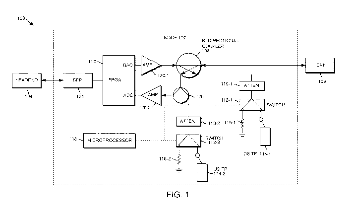
I 0025] FIG. 1 depicts a simplified system 100 that terminates ports in a bi-
directional coupler
according to some embodiments. System 100 includes a node 102, a head end 104,
and customer
premise equipment (CPE) 106. In some embodiments, node 102 is separate from
headend 104.
However, components of node 102 may also be included in head end 104. In some
cases, an
operator would like to have a test point inserted in both directions so that
the operators can check
system level performance without interrupting the operation of a live network.
Although the
following network is described, some embodiments may be used in other network
configurations,
such as WiFi or wireless networks.
CA 03117005 2021-04-19
WO 2020/081807 PCT/US2019/056729
(0026) In a full duplex design, the downstream connection and the upstream
connection may use
the same spectrum. A single bi-directional coupler 108 may be used to couple
the downstream
signal to downstream components for processing and also couple the upstream
signal to the
upstream components for processing. Using the bi-directional coupler 108 is
different from using
a separate coupler for the upstream direction and a separate coupler for the
downstream direction
as described in the Background.
(0027) In the downstream direction, head end 104 may send a signal to node
102, such as a digital
signal through a digital medium. In some embodiments, the signal may be
programming for a
cable television system; however, other content may be sent. In other
examples, head end 104
may send an analog signal through an analog medium to node 102.
[0028] A small-form pluggable transceiver (SFP) 124 may receive the downstream
signal. In
some embodiments, the transceiver may be a regular SFP digital transceiver or
an enhanced SFP
transceiver (SFP+) that may have more bandwidth capabilities then the regular
SFP transceiver.
Also, an analog signal may be received and processed by an analog receiver.
100291 A field programmable logic gate array (FPGA) 112 receives the signal
and can convert the
downstream signal using a digital-to-analog converter (DAC) from the digital
signal to an analog
signal. An amplifier 120-1, such as an RF amplifier, amplifies the analog
signal and sends the
analog signal to bi-directional coupler 108. Bi-directional coupler 108 may
then couple the
downstream signal to CPE 106, which may be a cable modem or other subscriber
device. CPE
106 receives the signal and can output the signal, such as to a subscriber
device.
100301 In the upstream direction, CPE 106 may send an upstream signal to node
102. The
upstream signal may be an analog signal. Bi-directional coupler 108 may couple
the upstream
signal through a splitter 126. Splitter 126 splits the signal and sends the
signal to an amplifier,
such as an RF amplifier 120-2. After amplifying the analog signal, FPGA 122
may use an analog-
to-digital converter (ADC) to convert the analog signal to a digital signal.
The digital signal is
sent through SFP 124 to head end 104. In other examples, node 102 may send an
analog signal.
6
CA 03117005 2021-04-19
WO 2020/081807 PCT/US2019/056729
10031] In some embodiments, test points may be inserted into an upstream
connection or a
downstream connection in node 102. For example, node 102 may have a test point
connector (e.g.,
slot or other connection device) in which test points can be inserted. When
the term inserted is
used, the insertion may be any type of connection that can be made with a test
point 114. For
example, test point 114 may be inserted in a slot, connected to a connection
pad, etc. When
inserted, test point 114 may be connected to a board, such as an integrated
circuit board, in which
test point 114 is now operational and powered on.
10032] When inserted, the test points may be used to test the connection. An
upstream test point
(US TP) 114-2 may be used to test the connection (e.g., bandwidth or other
performance metrics)
in the upstream direction, which is from CPE 106 to head end 104 through node
102. A
downstream test point (DS TP) 114-1 may be used to test the connection of a
downstream
connection from head end 104 to CPE 106 through node 102. Downstream test
point 114-1 and
upstream test point 114-2 may or may not be inserted into a test point
connector. That is, both
downstream test point 114-1 and upstream test point 114-2 may be connected,
both downstream
test point 114-1 and upstream test point 114-2 may not be connected,
downstream test point 114-
1 may be connected, but upstream test point 114-2 may not be connected, and
upstream test point
114-1 may be connected, but downstream test point 114-1 may not be connected.
10033] When downstream test point 114-1 is inserted into a downstream test
point connector of
bi-directional coupler 108, bi-directional coupler 108 may couple to the
downstream signal to
downstream test point 114-1 at a downstream test point port. For example, bi-
directional coupler
108 may couple the downstream signal through attenuator 110-1, a switch 112-1
(e.g., an RF
switch) to downstream test point 114-1. Although attenuation of the signal may
be performed,
attenuation may not be needed.
10034] When downstream test point 114-1 is not inserted in a test point
connector, a termination
load 116-1 is connected to bi-directional coupler 108 at the downstream test
point port. For
example, the downstream test point port is connected through attenuator 110-1,
switch 112-1 to
termination load 116-1, which may be a 75-ohm load. The 75-ohm load may match
the load of
upstream test point 114-2 or termination load 116-2. The matching of the loads
provides maximum
directivity for bi-directional coupler 108.
7
CA 03117005 2021-04-19
WO 2020/081807 PCT/US2019/056729
[0035] When an upstream test point 114-2 is inserted into an upstream test
point connector of bi-
directional coupler 108, the upstream signal is sent from the upstream test
point port of bi-
directional coupler 108 through splitter 126. Splitter 126 splits the signal
and sends the signal to
attenuator 110-2 and switch 112-2 to upstream test point 114-2.
100361 When upstream test point 114-2 is not connected to a test point
connector, switch 112-2
switches to connect termination load 116-2 to the upstream test point port.
For example, the
upstream test point port is connected through attenuator 110-2, switch 112-2
to termination load
116-2, which may be a 75-ohm load. The 75-ohm load may match the load of
downstream test
point 114-1 or termination load 116-1. The matching of the loads also provides
maximum
directivity for bi-directional coupler 108.
[0037] A microprocessor 118 may control switch 112-2 to couple the upstream
test point port to
upstream test point 114-2 or termination load 116-2. Also, microprocessor 118
may control switch
112-1 to couple downstream test point 114-1 and termination load 116-1 to the
downstream test
point port. Microprocessor 118 may analyze whether or not downstream test
point 114-1 or
upstream test point 114-2 is inserted in a respective test point connector to
determine the position
of switch 112-1 and 112-2, respectively.
[0038] Bi-directional coupler
100391 FIG. 2 depicts a more detailed example of bi-directional coupler 108
according to some
embodiments. Bi-directional coupler 108 includes a first port 202, a second
port 204, a
downstream test point (TP) port 206 and an upstream test point (TP) port 208.
First port 202 and
second port 204 may be both used for the upstream signal and the downstream
signal. For
example, when bi-directional coupler 108 is coupling the downstream signal
downstream, first
port 202 is an input downstream port that receives the downstream signal and
second port 204 is
an output downstream port that outputs the downstream signal. When bi-
directional coupler 108
is coupling the upstream signal upstream, second port 204 is an input upstream
port that receives
the upstream signal and first port 202 is an output upstream port that outputs
the upstream signal.
8
CA 03117005 2021-04-19
WO 2020/081807 PCT/US2019/056729
(0040) Switch 112-2 can switch between termination load 116-2 and upstream
test point 114-2.
As shown, both upstream test point 114-2 and termination load 116-2 may have a
75-ohm load.
Although a 75-ohm load is used, the load may be different values. For example,
load impedance
is 75 ohm for a 75 ohm system (e.g., cable television networks) and 50 ohm for
a 50 ohm system
(e.g., a WiFi or a wireless system). However, termination load 116-2 may have
the same load (or
very similar within a threshold) as downstream test point 114-1 to provide the
maximum isolation
and maximum directivity when upstream test point 114-2 is not connected to
upstream test point
port 208.
100411 Switch 112-1 may also switch between termination load 116-1 and
downstream test point
114-1. Similarly, termination load 116-1 and downstream test point 114-1 have
the same load of
75-ohms. Termination load 116-1 may have the same load (or very similar within
a threshold) as
upstream test point 114-2 to provide the maximum isolation and directivity
when test point 114-1
is not connected to downstream test point port 206.
100421 As discussed above, different combinations of which test points are
inserted into test point
connections may be appreciated. FIGs. 3A, 3B, and 3C show different
connections for bi-
directional coupler 108 according to some embodiments. FIG. 3A shows the
downstream
connection without upstream test point 114-2 connected to bi-directional
coupler 108 according to
some embodiments. Downstream test point 114-1 has been inserted into a test
point connector
and is connected to bi-directional coupler 108.
10043] Input downstream port 202 receives a downstream signal and the
downstream signal is
coupled to output downstream port 204. Also, the downstream signal is coupled
to downstream
test point port 206 because switch 112-1 is switched to downstream test point
114-1. Accordingly,
termination load 116-1 is not connected to bi-directional coupler 108.
[0044] Upstream test point port 208 is also coupled to output downstream port
204. This port
needs to be properly terminated to provide maximum isolation in the downstream
direction. In
this example, upstream test point 114-2 is not inserted in a test point
connector. Accordingly,
switch 112-2 is switched to couple termination load 116-2 to upstream test
point port 208 thereby
9
CA 03117005 2021-04-19
WO 2020/081807 PCT/US2019/056729
terminating upstream test point port 208 and not leaving an open port.
Termination load 116-2 is
the same load as downstream test point 114-1 to provide maximum directivity.
100451 FIG. 3B shows the upstream connection without downstream test point 114-
1 connected to
bi-directional coupler 108 according to some embodiments. Input upstream port
204 receives an
upstream signal and couples the upstream signal to output upstream port 202.
Also, input upstream
port 204 couples the upstream signal to upstream test point port 208. Upstream
test point 114-2
has been inserted into a test point connector and is connected to bi-
directional coupler 108 via
switch 112-2. Accordingly, termination load 116-2 is not connected to bi-
directional coupler 108.
[00461 Also, output upstream port 202 is coupled to downstream test point port
206. This port
needs to be properly terminated to provide maximum isolation in the upstream
direction. In this
example, downstream test point 114-1 is not inserted in a test point
connector. Accordingly, switch
112-1 is switched to couple termination load 116-1 to downstream test point
port 206 thereby
terminating downstream test point port 206. Termination load 116-1 is the same
load as upstream
test point 114-2 to provide maximum directivity.
[00471 FIG. 3C shows a connection with both downstream test point 114-1 and
upstream test point
114-2 connected to bi-directional coupler 108 according to some embodiments.
Since both
downstream test point 114-1 and upstream test point 114-2 are inserted into a
respective test point
connector, termination loads are not needed. Switch 112-1 connects downstream
test point 114-1
to downstream test point port 206 and switch 112-2 connects upstream test
point 114-2 to upstream
test point port 208. Both test points 114-1 and 114-2 are the same load and
provide maximum
directivity for bi-directional coupler 108.
100481 In some embodiments, both downstream test point 114-1 and upstream test
point 114-2
may not be inserted into test point connectors. In this example, switch 112-1
is connected to
termination load 116-1 and switch 112-2 is connected to termination load 116-
2.
100491 Different examples of detection mechanisms
100501 The following describes some examples of detection mechanisms. Although
these
examples of detection mechanisms are described, other examples of detection
mechanisms may
CA 03117005 2021-04-19
WO 2020/081807 PCT/US2019/056729
be used. FIGs. 4A and 4B show a sensor 402 being used to detect when a test
point is inserted
into a test point connector 408 according to some embodiments. In FIG. 4A,
sensor 402, such as
a light sensor, can detect a signal, such as light. Sensor 402 may be located
in test point connector
408 in which a test point 114 may be inserted. For example, sensor 402 may be
on a circuit board
in which test point 114 may be inserted to connect to test point connector
408.
[0051] Node 102 includes an emitter, such as light emitter 404, that emits the
signal, such as light,
which may be detected by sensor 402. For example, light may reflect off a
surface 406 in node
102 to sensor 402. However, in other examples, the light may not need to be
reflected off a surface.
Rather, the light may be emitted directly to sensor 402.
100521 FIG. 4B shows an example when a test point 114 is inserted into test
point connector 408
according to some embodiments. When test point 114 is inserted into test point
connector 408,
test point 114 becomes operational as in test point 114 can test network
characteristics for node
102. However, test point 114 needs to be coupled to a port of bi-directional
coupler 108. When
the light emitted by emitter 404 is blocked from reaching light sensor 402,
light sensor 402 may
output a signal indicating that test point 114 has been inserted in test point
connector 408. In some
embodiments, the light may be blocked test point 114 thereby blocking the
light from reaching
light emitter 404. Microprocessor 118 uses the signal from light sensor 402 to
change a position
of switches 112-1 and/or 112-2 to couple a test point 114 to upstream test
point port 208 and/or
downstream test point port 206 as described above.
I 0053] FIGs. 5A and 5B depict an example of a push-button switch according to
some
embodiments. In FIG. 5A, push-button switch 502 may be a structure that can be
actuated by
contact. For example, the push-button switch may be pushed in a direction,
such as downward or
parallel to the insertion direction of test point 114. Push-button switch 502
may be located at the
bottom of test point connector 408. However, push-button switch 502 may also
be located at other
locations, such as the side of test point connector 408. Also, push-button
switch 502 may be
actuated in any direction, such as parallel to a circuit board or
perpendicularly to test point 114.
[0054] In FIG. 5B, when test point 114 is inserted into test point connector
408, push-button switch
502 is actuated in a downward direction. When push-button switch 502 is
actuated, such as past a
11
CA 03117005 2021-04-19
WO 2020/081807 PCT/US2019/056729
threshold, then push-button switch 502 outputs a signal indicating test point
114 has been inserted
into test point connector 408. The signal from push-button switch 502 may be
used to change
switches 112-1 and/or 112-2 to couple test point 114 to upstream test point
port 208 and/or
downstream test point port 206 as described above.
100551 FIGs. 6A and 6B depict an example of a hinge roller lever switch
according to some
embodiments. In FIG. 6A, hinge folder lever switch 602 may include a lever
that can be actuated
in a direction. Hinge folder lever switch 602 may be located on a side of test
point connector 1208.
A lever with a roller is placed proximate to test point connector 1208 such
that a test point 114
will contact the roller when inserted in test point connector 1208.
100561 In FIG. 6B, test point 114 has been inserted into test point connector
1208. At 604, the
lever of hinge folder lever switch has been moved in a direction that
depresses a button. When
inserted, test point 114 moves the roller lever in a direction to actuate a
button, such as to depress
a button on hinge roller lever switch 602. When the button is depressed, hinge
roller lever switch
602 outputs a signal indicating test point 114 has been inserted into test
point connector 1208. The
signal from hinge folder lever switch 602 may be used to change switches 112-1
and/or 112-2 to
couple test point 114 to upstream test point port 1008 and/or downstream test
point port 1006 as
described above.
12
CA 03117005 2021-04-19
WO 2020/081807 PCT/US2019/056729
(0057) Switch control
[0058) As discussed above, each implementation sent a signal that caused a
switch to couple test
point 114 to bi-directional coupler 108. FIG. 7 depicts the signaling to
control switches 112
according to some embodiments. Node 102 includes a detection mechanism 702-1
that detects
whether downstream test point 114-1 is inserted into test point connector 408
and a detection
mechanism 702-2 that detects whether upstream test point 114-2 is inserted
into test point
connector 408. Detection mechanism 702-1 or 702-2 may be one of the detection
mechanisms
described above or may be a different one. When either detection mechanism 702-
1 or 702-2
detects the insertion of a test point 114-1 or 114-2, respectively, detection
mechanism 702-1 or
702-2 sends a signal to microprocessor 118.
[0059] Microprocessor 118 processes the signal and determines that a test
point has been inserted
into a respective test point connector 408. Once the test point is inserted
into the test point
connector 408, microprocessor 118 communicates with switch 112-1 or switch 112-
2. For
example, when downstream test point 114-1 is inserted into a test point
connector 408-1,
microprocessor 118 sends a signal to switch 112-1 to couple downstream test
point port 206 to
downstream test point 114-1. Similarly, when microprocessor 118 detects that
test point 114-2 is
inserted into a test point connector 408-2, microprocessor 118 sends a signal
to switch 112-2 to
couple test point connector 114-2 to upstream test point port 208.
100601 FIG. 8 depicts a simplified flowchart 800 of a method for controlling
switches according
to some embodiments. At 802, microprocessor 118 detects an insertion of a test
point 114 in test
point connector 408. At 804, microprocessor 118 determines which test point
114 has been
inserted. For example, microprocessor 118 may determine whether an upstream
test point 114-2
or a downstream test point 114-1 has been inserted. At 806, when a downstream
test point 114-1
has been inserted, microprocessor 118 changes switch 112-1 from termination
load 116-1 to
downstream test point 114-1.
100611 At 808, when an upstream test point 114-2 has been inserted,
microprocessor 118 changes
switch 112-2 from termination load 116-2 to upstream test point 114-2.
Accordingly, instead of
13
CA 03117005 2021-04-19
WO 2020/081807 PCT/US2019/056729
having an open port when a test point is not inserted in a test point
connector, some embodiments
couple a termination load to provide better isolation for bi-directional
coupler 108.
100621 Described herein are techniques for a power supply control system. In
the following
description, for purposes of explanation, numerous examples and specific
details are set forth in
order to provide a thorough understanding of some embodiments. Some
embodiments as defined
by the claims may include some or all of the features in these examples alone
or in combination
with other features described below, and may further include modifications and
equivalents of the
features and concepts described herein.
[00631 Some embodiments control a power supply voltage being applied to a slot
in a node based
on the type of module that is inserted into the slot. For example, the slot
may be configured to
receive a first type of module, such as an analog small-form pluggable (SFP)
module. The analog
SFP module may be configured to operate with a first power supply voltage,
such as a +5V power
supply. In some embodiments, a processor for the node may set the default
power supply voltage
to a second power supply voltage that is different from the first power supply
voltage. For
example, a lower power supply voltage, such as a +3.3V power supply voltage,
may be set as the
default power supply voltage to apply to the slot. The +3.3V power supply
voltage may be the
voltage that a second type of SFP module, such as a digital SFP module, is
configured to use or
may be a voltage that will not damage the digital SFP module. Thus, if a
digital SFP module is
accidentally plugged into the slot, the digital SFP module will not be damaged
by the power supply
voltage of 3.3V. However, if a +5V power supply voltage is being applied to
the power supply
pin of the digital SFP module, the voltage would damage the digital SFP module
because the digital
SFP module is not configured to operate with a +5V voltage. The higher voltage
could damage
some components of the digital SFP module.
[00641 To control the power supply voltage, when a module is inserted into a
slot of the node, the
processor detects the insertion of the module. Then, the processor
communicates with the module
to determine which type of module has been inserted into the slot. For
example, the processor may
receive information from the module and use the information to determine
whether the module is
a digital SFP module or an analog SFP module. Then, the processor may
determine the appropriate
14
CA 03117005 2021-04-19
WO 2020/081807 PCT/US2019/056729
power supply voltage for the module. For example, the processor can use the
+3.3V power supply
voltage for a digital SFP module and a +5V power supply voltage for an analog
SFP module.
100651 The processor adjusts the power supply voltage being supplied to the
power supply pin of
the slot to +5V when the analog SFP is detected. However, if the digital SFP
module has been
inserted into the slot, the processor does not change the power supply
voltage.
100661 FIG. 9 depicts a simplified system 100 for a network in which a power
supply voltage is
controlled according to some embodiments. System 900 includes a headend 906, a
node 902, and
customer premise equipment (CPE) 904. Headend 906 and node 902 may be
separated by a
network, such as a digital network, (e.g., an Ethernet or an optical network)
and/or analog network
(e.g., a radio frequency (RF) network). Node 902 may be located closer to the
premises of a
subscriber compared to headend 906. The premises of the subscriber includes a
network device,
such as a CPE 904 (e.g., a cable modem, subscriber device, set-top-box,
gateway, etc.). Although
this architecture is described, other distributed architectures may be used.
Further, the components
of node 902 could be located in headend 906.
10067] In a downstream direction, headend 906 sends a digital signal over a
digital medium, such
as Ethernet or a passive optical network (PON), to node 902. The digital
signal is received as
electrical signals at a remote physical device in node 902. The remote
physical device may be
considered the node 902 or be part of node 902 and include the components
shown. However, for
discussion purposes, the term node 902 will be used. Node 902 converts the
digital signal to an
analog signal, such as a radio frequency (RF) signal.
100681 Node 902 may also receive an analog signal from headend 106 over an
analog medium.
Node 902 may then combine the analog signal from the analog medium with the
analog signal that
was converted from the digital signal from the digital medium. Node 902 sends
the combined
analog signal (e.g., an RF signal) over an analog medium, such as a coaxial
network, to CPE 904.
10069] In an upstream direction, CPE 104 may also transmit an analog signal to
node 902 via the
analog medium. The analog signal may include portions for transmission through
both the digital
medium and the analog medium to headend 106. Node 902 then converts at least a
portion of the
CA 03117005 2021-04-19
WO 2020/081807 PCT/US2019/056729
analog signal to a digital signal and sends the digital signal to headend 906
through the digital
medium. Additionally, node 902 sends at least a portion of the analog signal
to headend 906
through the analog medium.
10070j The processing of the analog signal and digital signal within node 902
will now be
discussed in more detail. Different SFP modules may be used to receive and
transmit digital and
analog signals. An SFP module is a module that can be inserted into a slot in
node 902. Although
small form pluggable modules are described, other types of modules that can be
inserted into areas
of node 902 may be used. A first SFP module is configured to receive and send
a digital signal
and a second SFP module is configured to receive, process, and send an analog
signal. In some
examples, an analog SFP module cannot receive, process, and send a digital
signal, and a digital
SFP module cannot receive and send an analog signal.
100711 In the downstream direction, node 902 may receive an analog signal at
an analog SFP
receiver, such as an SFP-RF receiver (Rx) 908. Node 902 may also receive a
digital signal at a
digital SFP transceiver, such as an SFP transceiver 110. The digital SFP may
be a regular SFP or
enhanced SFP+ and may send digital signals both upstream and downstream. A
regular digital
SFP may support a first amount of gigabits (Gbits) per second of
communication. An enhanced
SFP (SFP+) may be an enhanced version of the SFP and may support data rates
that are higher
than the regular SFP, such as 16Gbit/s. Although the enhanced version will be
used for discussion
purposes, other SFP types may also be appreciated.
10072j The digital signal is processed by a field programmable gate array
(FPGA) 914 that sends
the digital signal to a digital to analog converter (DAC) 916 that converts
the digital signal to an
analog signal. The analog signal from SFP-RF Rx 908 and the digital signal
from DAC 916 may
be combined in a combiner 920. The analog signal is overlaid with the digital
signal in the
combined analog signal output by combiner 920. The combined signal may then be
amplified by
an amplifier 924 and transferred through a device 928 that can then output the
analog signal to
CPE 904. Transfer device 928 can combine an upstream signal with downstream
signal. For
example, device 928 may be a diplexer filter that can multiplex signals from
two ports to a single
port, such as the upstream bandwidth is from 5 to 42 or 85 MHz, and downstream
is from 54 or
16
CA 03117005 2021-04-19
WO 2020/081807 PCT/US2019/056729
108 MHz to .12 GHz. Also, device 928 may be a coupler that can couple either
the upstream
signal or the downstream signal in either direction.
100731 In the upstream direction, CPE 904 may transmit an analog signal to
node 902. Transfer
device 928 sends the analog signal to amplifier 926 for amplification. The
analog signal is input
into a splitter 922. The analog signal includes a digital portion and an
analog portion that may be
split at splitter 922. The analog portion is sent to an analog SFP
transmitter, such as SFP-RF
transmitter (Tx) 912. SFP-RF Tx 912 then sends the analog signal to head end
906.
[0074] For the digital portion of the upstream signal, an analog-to-digital
converter (ADC) 918
receives the digital portion of the upstream signal and converts the analog
signal to digital. FPGA
914 receives the digital signal and provides the digital signal to digital SFP
910. SFP 910 can then
send the digital signal to head end 906.
10075] Although the above network configuration is described, it will be
understood that other
network configurations may be used. Also, other components not shown in node
902 may also be
used to process the analog and digital signals.
[0076] FIG. 10 depicts a more detailed example of node 902 according to some
embodiments.
Node 902 includes multiple slots 202-1 to 202-3. Although three slots are
shown, node 902 may
have a different number of slots, such as 2 slots, 4 slots, 5 slots, etc.
Slots 1002-1 to 1002-3 may
be specifically configured to operate with a specific type of SFP module. In
some examples, slot
1002-1 is configured to operate with SFP-RF Rx 908; slot 1002-2 is configured
to operate with
digital SFP+ 910; and slot 1002-3 is configured to operate with SFP-RF Tx 912.
By operate, each
slot when receiving the correct SFP module, can communicate data appropriately
in the upstream
and/or downstream directions. When a wrong SFP module is inserted into a slot
1002, that module
will not process and transmit signals in node 902 properly. For example, a
digital SFP module
that is inserted into an analog SFP module slot will not properly process and
transmit the analog
signal that is received at that slot. Although this configuration is
described, other configurations
of slots may be appreciated.
17
CA 03117005 2021-04-19
WO 2020/081807 PCT/US2019/056729
[0077] Each slot 1002 includes pin connectors 1004 in which pins from an SFP
module can be
coupled, such as inserted. Pin connectors may be individual connection points
that can receive
and connect to pins of SFP modules. In some examples, the pin layout
dimensions for each slot
1002-1 to 1002-3 is similar or the same. The same may be using identical
dimensions when
designing the pin layout. The pin layout may be the same dimension-wise, such
as the pin
connectors are in the same position in the layout, such as in the same spacing
arrangement. The
connectors are the same in that they can fit both the analog SFP module and
the digital SFP module.
That is, the number of the pins and layout of the pins and spacing of the pins
can receive either the
pins of the analog SFP module or the digital SFP module. Further, the
connectors may be
configured to receive the same type of pins. That is, at least a portion of
the pins may be configured
to perform similar functions, such as both the analog SFP module and the
digital SFP module have
a power supply pin in the same position. The packaging of the analog SFP
module or the digital
SFP module may also look similar. That is, a design of both packages may use
similar or the same
specifications.
100781 FIG. 11 depicts a more detailed example of node 102 according to some
embodiments. A
processor 1102 may configure FPGA 914, DAC 916, ADC 918, transfer device 928,
and other
components in node 902 based on different requirements. Some embodiments
leverage processor
1102 to adjust a power supply voltage based on what type of SFP module is
inserted into a slot.
For example, processor 1102 is configured to communicate with an SFP module
1112 that has
been inserted into a slot 1002. Processor 1102 controls a power supply 310
that can output a first
power supply voltage or a second power supply voltage, such as a 5.0V or 3.3V
power supply
voltage, based on which type of SFP module has been inserted into slot 1002.
The described
process may be performed for each slot that is configured to receive an analog
SFP module.
100791 When SFP module 1112 is inserted into slot 202, processor 1102 senses
the insertion via a
status line. For example, the status line may be a MOD ABS line that senses
when a SFP module
1112 is inserted into a slot 1002. In some examples, the status line is
coupled to a pin connector
#6, and SFP module 1112 sends a signal through the status line to a module
sensor 1108. The
signal indicates to module sensor 908 that an SFP module has been inserted
into slot 1002.
18
CA 03117005 2021-04-19
WO 2020/081807 PCT/US2019/056729
(0080) Module sensor 1108 detects the insertion and causes a power supply
controller 1106 to
determine which power supply voltage to supply to SFP module 1112. In some
examples, power
supply controller 1106 communicates through a bus, such as an I2C bus that is
connected to a
connector of slot 1002 and pin of SFP module 1112. In some examples, the bus
is connected to a
pin #3 of SFP module 1112. Through the communication, power supply controller
1106 may
receive information regarding the type of SFP module 1112 along with other
information. For
example, SFP module 1112 may send information in an address space of the bus,
which may be
divided into lower and upper 128 bytes. SFP module 1112 may send the
information in one part
of the address space, such as the lower 128 bytes of the address space. The
information may
include the SFP type (e.g., whether the SFP module 312 is a digital SFP/SFP+
module or an analog
SFP module). Other information may include the name of the SFP manufacturer
and bias voltage,
such as whether the SFP module 1112 requires a power supply voltage of 5V or
3.3V.
100811 FIG. 12 depicts a simplified flowchart 1200 of a method for determining
whether a module
inserted into a slot 1002 is an analog SFP module or a digital SFP module
according to some
embodiments. At 1202, processor 1102 receives a signal that a module is
inserted into slot 1002.
At 1204, processor 1102 receives a status signal for the SFP module. At 1206,
processor 1102
may review a portion of the address space in the status signal. For example,
information needed
to determine whether the SFP module is an analog SFP module or a digital SFP
module may be
included in a portion of the 256 bytes of the bus address space. Processor 302
can detect the bytes
in a 128 bit address space and determine whether the SFP module is a digital
SFP module or an
analog SFP module. Also, processor 1102 may determine the bias voltage
specified for the SFP
module. Determining the bias voltage may allow processor 1102 to use a
specified power supply
voltage for the SFP module 1112. For example, processor 1102 may dynamically
configure the
power supply voltage for different SFP modules to multiple values (e.g., more
than two values).
This may allow more flexibility for configuring the power supply voltage
rather than having two
power supply voltages for an analog SFP and a digital SFP module.
100821 Referring back to FIG. 11, power supply controller 1106 may send a
power supply control
message to power supply 1110 when power supply controller 1106 detects that
SFP module 1112
is an analog SFP module. This is because by default, power supply 1110 may
output a 3.3V power
19
CA 03117005 2021-04-19
WO 2020/081807 PCT/US2019/056729
supply voltage (or some other voltage lower than 5V or 3.3V) to SFP module
1112. In some
embodiments, the power supply voltage may be output to pin 16 of SFP module
1112, which may
be the power supply pin for both the analog SFP module and the digital SFP
module. Power supply
controller 1106 can send a signal to power supply 1110 to increase the power
supply voltage being
output from 3.3V to 5.0V. Power supply 1110 can then receive the input 5.3V
signal and then
output the 5.0V signal instead of the 3.3V signal. Then, the analog SFP module
then receives the
proper power supply voltage for its specification.
10083] If the SFP module 1112 was a digital SFP module, then power supply
controller 1106 may
not change the voltage output by power supply 1110. Although 3.3V voltage may
be used as the
default voltage, power supply 1110 may output other voltages as the default
voltage. For example,
in other examples, the default voltage may be lower than 3.3V and power supply
controller 1106
can increase the voltage to 3.3V upon determining that the digital SFP module
has been inserted
into slot 1002. In all cases, when an analog SFP module is inserted into slot
1002, power supply
controller 1106 can increase the default voltage to 5.0V (or whatever the
specified voltage is for
the analog SFP module).
[00841 Accordingly, when a digital SFP module 1112 is inserted into a slot
that is configured for
an analog SFP module, the digital SFP module will not be damaged by a power
supply voltage
that is higher than the digital SFP module is configured to receive. However,
when an analog SFP
module is correctly inserted into a slot for an analog SFP, processor 1102 can
increase the power
supply voltage to the configured amount for the analog SFP. Digital SFPs that
have the same
packaging as analog SFPs, and may be mistakenly inserted into analog SFP
slots, are thus not
damaged. In some examples, analog SFPs will not be damaged if inserted into a
digital SFP slot.
Thus, processor 1102 may not have a process to detect and change any power
supply voltage for
the slots configured to receive digital SFPs.
100851 FIG. 13 depicts a simplified flowchart 1300 of a method for managing
power supply
voltages for a slot 1002 according to some embodiments. As discussed above,
the digital slots
may not need to be managed as an analog SFP module that is inserted into a
digital slot may not
be damaged by the power supply voltage provided to that slot 202. At 1302,
processor 1102 sets
the power supply voltage output by power supply 1110 to a default voltage,
such as 3.3V. Then,
CA 03117005 2021-04-19
WO 2020/081807 PCT/US2019/056729
at 1304, processor 1102 detects insertion of an SFP module 1112 in slot 1002.
The detection may
be through a status line that is connected to a pin of SFP module 1112.
100861 At 1306, processor 1102 determines whether or not the SFP module
inserted into slot 1002
is an analog SFP. If not, then at 1308, processor 1102 keeps the power supply
voltage at 3.3V.
For example, processor 1102 may not perform any actions to change the power
supply voltage.
100871 If processor 1102 detects that an analog SFP module was inserted into
slot 1002, at 1310,
processor 1102 sends a signal to power supply 1110 to increase the voltage to
5.0V. Then, power
supply 1110 increases the voltage from 3.3V to 5.0V, which is the configured
voltage for an analog
SFP module. The analog SFP module may then transmit or receive the analog
signal as configured.
[0088] At 1312, processor 1102 monitors for removal of the SFP module 1112. At
1314, processor
1102 determines if SFP module 312 was removed. When the SFP module 1112 was
removed, at
1316, processor 1102 changes the power supply voltage back to 3.3V. The
changing of the power
supply voltage back to 3.3V may be immediately performed to ensure that
another SFP module
1112 that is inserted into slot 1002 may not be a digital SFP module, which
can be damaged by
the higher power supply voltage.
10089] Accordingly, some embodiments provide protection for a slot 1002 that
may receive SFP
modules that may not be configured for the slot. Due to having digital SFP
modules and analog
SFP modules being manufactured having similar packaging and a similar pin
layout, it is possible
that a slot 1002 may have an SFP module inserted into it that is not
configured to be inserted into
that slot. Since the power supply pin for both modules is connected to the
same connector, the
higher voltage for the analog SFP module may damage the digital SFP module.
Not damaging an
erroneously inserted digital SFP module will save large replacement costs.
Leveraging processor
1102 to control power supply 1110 in node 902 requires minimal cost because
processor 1102 is
being used to configure other components of node 102, but the control of power
supply 1110 saves
a large cost when mistakes are made by inserting a wrong SFP module into a
slot 1002.
21
CA 03117005 2021-04-19
WO 2020/081807 PCT/US2019/056729
System
[0090] FIG. 14 illustrates an example of special purpose computer systems 900
configured with
node 102 according to one embodiment. Computer system 1400 includes a bus
1402, network
interface 1404, a computer processor 1406, a memory 1408, a storage device
1410, and a display
1412.
100911 Bus 1402 may be a communication mechanism for communicating
information. Computer
processor 906 may execute computer programs stored in memory 1408 or storage
device 1408.
Any suitable programming language can be used to implement the routines of
some embodiments
including C, C++, Java, assembly language, etc. Different programming
techniques can be
employed such as procedural or object oriented. The routines can execute on a
single computer
system 1400 or multiple computer systems 1400. Further, multiple computer
processors 1406 may
be used.
100921 Memory 1408 may store instructions, such as source code or binary code,
for performing
the techniques described above. Memory 1408 may also be used for storing
variables or other
intermediate information during execution of instructions to be executed by
processor 1406.
Examples of memory 1408 include random access memory (RAM), read only memory
(ROM), or
both.
100931 Storage device 1410 may also store instructions, such as source code or
binary code, for
performing the techniques described above. Storage device 1410 may
additionally store data used
and manipulated by computer processor 1406. For example, storage device 1410
may be a
database that is accessed by computer system 900. Other examples of storage
device 1410 include
random access memory (RAM), read only memory (ROM), a hard drive, a magnetic
disk, an
optical disk, a CD-ROM, a DVD, a flash memory, a USB memory card, or any other
medium from
which a computer can read.
10094] Memory 1408 or storage device 1410 may be an example of a non-
transitory computer-
readable storage medium for use by or in connection with computer system 1400.
The non-
transitory computer-readable storage medium contains instructions for
controlling a computer
22
CA 03117005 2021-04-19
WO 2020/081807 PCT/US2019/056729
system 1400 to be configured to perform functions described by some
embodiments. The
instructions, when executed by one or more computer processors 1406, may be
configured to
perform that which is described in some embodiments.
10095] Computer system 1400 includes a display 1412 for displaying information
to a computer
user. Display 1412 may display a user interface used by a user to interact
with computer system
1400.
[0096] Computer system 1400 also includes a network interface 1404 to provide
data
communication connection over a network, such as a local area network (LAN) or
wide area
network (WAN). Wireless networks may also be used. In any such implementation,
network
interface 1404 sends and receives electrical, electromagnetic, or optical
signals that carry digital
data streams representing various types of information.
100971 Computer system 1400 can send and receive information through network
interface 1404
across a network 1414, which may be an Intranet or the Internet. Computer
system 1400 may
interact with other computer systems 1400 through network 1414. In some
examples, client-server
communications occur through network 1414. Also, implementations of some
embodiments may
be distributed across computer systems 1400 through network 1414.
100981 Some embodiments may be implemented in a non-transitory computer-
readable storage
medium for use by or in connection with the instruction execution system,
apparatus, system, or
machine. The computer-readable storage medium contains instructions for
controlling a computer
system to perform a method described by some embodiments. The computer system
may include
one or more computing devices. The instructions, when executed by one or more
computer
processors, may be configured to perform that which is described in some
embodiments.
100991 As used in the description herein and throughout the claims that
follow, "a", "an", and
"the" includes plural references unless the context clearly dictates
otherwise. Also, as used in the
description herein and throughout the claims that follow, the meaning of "in"
includes "in" and
"on" unless the context clearly dictates otherwise.
23
CA 03117005 2021-04-19
WO 2020/081807 PCT/US2019/056729
[Oft 001 The above description illustrates various embodiments along with
examples of how
aspects of some embodiments may be implemented. The above examples and
embodiments
should not be deemed to be the only embodiments, and are presented to
illustrate the flexibility
and advantages of some embodiments as defined by the following claims. Based
on the above
disclosure and the following claims, other arrangements, embodiments,
implementations and
equivalents may be employed without departing from the scope hereof as defined
by the claims.
Embodiments
[001011 Some embodiments may include detecting, by a computing device that
includes the
first slot and a second slot, a module that is inserted into the first slot of
the computing device,
wherein the first slot is configured to operate with a first type of module
and the second slot is
configured to operate with a second type of module, the first slot and the
second slot including a
same pin position for receiving a power supply pin from the first type of
module and the second
type of module; communicating, by the computing device, with the module to
determine whether
the module is the first type of module or the second type of module, the first
type of module
configured to receive a first type of signal that is combined with a second
type of signal from the
second type of module at the computing device; and adjusting, by the computing
device, a power
supply voltage to the power supply pin of the first slot from a first value to
a second value when
the first type of module is detected.
1001021 Some embodiments disclosed herein may also or instead include
setting the power
supply voltage to the first value before detecting the module being inserted
into the first slot. In
some embodiments the first value is a default value when no module is inserted
into the first slot.
Some embodiments may also or instead include detecting when the module is
removed from the
first slot of the computing device; and changing the power supply voltage from
the second value
to the first value. In some embodiments the first type of module and the
second type of module
have a same pin type arrangement. In some embodiments the first type of module
and the second
type of module have the same pin layout dimensions. In some embodiments the
first slot and the
second slot have a same pin type arrangement. In some embodiments the first
type of module and
the second type of module have a same packaging design.
24
CA 03117005 2021-04-19
WO 2020/081807 PCT/US2019/056729
[NI 031 In some embodiments the first type of module uses a higher power
supply voltage
than the second type of module. In some embodiments the first type of module
uses a 5 volt power
supply voltage and the second type of module uses a 3.3 volt power supply
voltage. In some
embodiments the first type of module is configured to receive an analog
signal; and the second
type of module is configured to receive a digital signal. Some embodiments may
include wherein
the computing device overlays the analog signal over an analog signal that is
converted from the
digital signal, and outputs the combined signal. Some embodiments may include
wherein adjusting
the power supply voltage comprises: outputting a signal to a power supply to
adjust the power
supply voltage to the second value.
1001041 Some embodiments may include wherein detecting the module is
inserted
comprises receiving a signal from a pin connected to the module indicating the
module is inserted
into the first slot. Some embodiments may include wherein communicating with
the module
comprises: receiving a signal from the module indicating a device type; and
analyzing the signal
to determine that the device type is the first type of module. Some
embodiments may include
wherein the first slot is not configured to operate with the second type of
module and process the
second type of signal.
[NI 051 Some embodiments may include a non-transitory computer-readable
storage
medium containing instructions that, when executed, control a computer system
to be configured
for detecting, in the computer system that includes a first slot and a second
slot, a module that is
inserted into the first slot of the computer system, wherein the first slot is
configured to operate
with a first type of module and the second slot is configured to operate with
a second type of
module, the first slot and the second slot including a same pin position for
receiving a power supply
pin from the first type of module and the second type of module; communicating
with the module
to determine whether the module is the first type of module or the second type
of module, the first
type of module configured to receive a first type of signal that is combined
with a second type of
signal from the second type of module at the computer system; and adjusting a
power supply
voltage to the power supply pin of the first slot from a first value to a
second value when the first
type of module is detected. Some embodiments may include the non-transitory
computer-readable
storage medium configured for setting the power supply voltage to the first
value before detecting
CA 03117005 2021-04-19
WO 2020/081807 PCT/US2019/056729
the module being inserted into the first slot. Some embodiments may include
the non-transitory
computer-readable storage medium further configured for detecting when the
module is removed
from the first slot of the computing device; and changing the power supply
voltage from the second
value to the first value.
1001061 Some embodiments may include an apparatus comprising: one or more
computer
processors; and a non-transitory computer-readable storage medium comprising
instructions, that
when executed, control the one or more computer processors to be configured
for: detecting, in
the apparatus that includes a first slot and a second slot, a module that is
inserted into the first slot
of the apparatus, wherein the first slot is configured to operate with a first
type of module and the
second slot is configured to operate with a second type of module, the first
slot and the second slot
including a same pin position for receiving a power supply pin from the first
type of module and
the second type of module; communicating with the module to determine whether
the module is
the first type of module or the second type of module, the first type of
module configured to receive
a first type of signal that is combined with a second type of signal from the
second type of module
at the apparatus; and adjusting a power supply voltage to the power supply pin
of the first slot from
a first value to a second value when the first type of module is detected.
Some embodiments may
include an apparatus capable of performing the method disclosed herein,
including the disclosed
features alone or in some combination.
26