Note : Les descriptions sont présentées dans la langue officielle dans laquelle elles ont été soumises.
Stackable photovoltaic module
The invention relates to a stackable photovoltaic module according to the
preamble of claim 1.
Photovoltaic modules convert the light from the sun into electrical energy.
The
module substantially consists of silicon-based solar cells that are mounted on
a
frame and covered by a glass plate. The storage and transport of the modules
have been difficult up to now because the modules are placed or stacked one on
top of the other. In particular, the modules must be prevented from slipping.
In
addition, the stacking creates a high total weight that has to be borne by the
lower
modules of the stack.
Some solutions for preventing the modules from slipping on one another are
already known from the prior art.
DE 10 2011 113 143 Al discloses a stacking bar with pressure relief for the
transport of solar modules. The stacking bar is a separate component which is
clamped onto the side of the solar module. In order to prevent the
photovoltaic
modules from slipping, the first stacking bar has a projection on the upper
side,
which engages in a recess in a second stacking bar. After the photovoltaic
module
has been installed, the stacking bar must either be disposed of or transported
to
the production site of the photovoltaic module for reuse, which is expensive.
DE102008051426A1 discloses a stackable photovoltaic module frame which
surrounds the periphery of the semiconductor component. The frame is designed
as a hollow profile and comprises so-called anti-slip elements. The anti-slip
elements are projections and recesses which engage in one another when a
plurality of frames are stacked one on top of the other. Furthermore, steps
are also
disclosed as anti-slip elements which, when stacked one on top of the other,
interact with the step above and thereby prevent the frames from slipping. The
anti-slip elements integrated into the frame all have angled, sharp edges.
Such
Date Recue/Date Received 2021-05-18
2
edges are good for preventing the frames from slipping on one another, but the
sharp edges can cause damage to the frame surface when the modules are
stacked.
EP 2 401 770 B1 discloses a device for photovoltaic modules that is suitable
for
transporting the modules. The device consists substantially of a hollow
chamber
profile which surrounds the periphery of the semiconductor component, the
semiconductor component being located in a U-shaped receiving portion in the
frame. The frame has different projections and recesses which engage in one
another when they are stacked one on top of the other.
Some of the above-mentioned devices have sharp edges which, when a plurality
of photovoltaic modules are stacked one on top of the other, cause damage to
the
module below. In addition, mounting the known hollow frame profiles on the
periphery of the semiconductor component is only possible with great effort.
The problem addressed by the invention is therefore that of simplifying the
mounting of a stackable photovoltaic module and, furthermore, of providing a
module which does not cause any damage when a plurality of modules are
stacked one on top of the other.
An essential feature is that the stackable photovoltaic module comprises a
frame
consisting of a plurality of frame elements which are connected by at least
one
connector.
The embodiment according to the invention is advantageous in that the
individual
frame elements can be easily plugged onto the side edges of the frameless
photovoltaic elements. The individual frame elements are then connected by the
connectors to form a surrounding frame.
In a first preferred embodiment, the frame consists of four frame elements
which
are connected by four connectors to form a square frame. The elongate frame
elements meet one another at a miter joint. This means that the two
intersections
Date Recue/Date Received 2021-05-18
3
of the frame elements meet at the same angle, which results in a smooth
transition
between the adjoining frame elements. In addition, the contact surfaces or
connection surfaces are enlarged and the stability of the connection between
the
two frame elements is increased.
In the preferred embodiment, the two frame elements have a miter joint having
a
450 angle. The butt joint of the two frame elements is in the region of the
corner
(edge) so that it is less noticeable. The corner connector then acts like a
miter
clamp, which fixes the two adjoining frame elements.
In a further preferred embodiment, a plurality of frame elements comprising a
plurality of miter joints are present on one side of the photovoltaic module.
The
individual frame elements are then connected by means of one connector each.
This is advantageous in that, in the case of particularly long photovoltaic
elements,
a plurality of frame elements can be arranged one behind the other, with no
transition between the individual frame elements being detectable due to the
miter
joints.
The frame elements are preferably connected by a connector. In the context of
the
present invention, a connector is understood to be any connection technology
which allows the two adjacent frame elements to be connected. The connector
can, for example, be designed as a corner connector having a 900 angle.
In a first preferred embodiment, the connectors are pressed into the hollow
chamber profile by means of press-in technology. Pressing-in takes place in
such
a way that the connectors on the PV modules are no longer visible in the
finished
state. However, it is also possible to arrange the connectors on the frame
elements by means of an adhesive connection, a welded connection or a screw
connection. A connector is understood to mean both a connector in the corner
region of the frame and a connector on the side face of the frame.
The connectors preferably have a nominal 4% oversize (e.g., 5.9 to 5.2 mm)
before the pressing-in process into the frame element, a connection being
Date Recue/Date Received 2021-05-18
4
achieved by means of a friction-welded connection between the connectors and
the frame elements. Other oversizes are also possible depending on the shape
or
type of frame elements. The connectors can also be compressed so as to have
undersize. The corner connector is inserted into the hollow profile of the
frame and
then mechanically "clinched" in the manufacturing process.
The frame element preferably has a U-shaped receiving portion which is plugged
onto the respective side edges of the solar cell or the photovoltaic element.
In a further preferred embodiment, the frame is designed as a hollow chamber
profile comprising a cavity which is enclosed at the edge and which can be
used
for laying cables and/or lines.
The frame element preferably has only rounded projections and rounded
depressions, which prevents damage to the other surfaces.
In a preferred embodiment, there is a rounded projection on the upper side of
the
frame element, i.e., on the highest point of the frame element. There is a
rounded
recess on the opposite side of the frame element. When a plurality of
photovoltaic
modules are stacked one on top of the other, the projection of the first frame
element now engages in the recess of a second frame element which is arranged
above the first frame element. The curves of the projection and the recess
preferably have certain tolerances which allow the projection to slide into
the
recess. In addition, the curves prevent sharp edges and thus reduce damage
when stacking. Owing to the special shape of the frame element, it is now
possible
to stack a plurality of photovoltaic modules, e.g., on pallets, one on top of
the
other, with loads being transferred carefully by means of the profiled frame
elements.
The profile of the frame element is designed in such a way that the individual
photovoltaic elements cannot come into contact when they are stacked one on
top
of the other. This is achieved by a profile web, which is located on the lower
side
of the frame element and partially extends in the longitudinal direction
toward the
Date Recue/Date Received 2021-05-18
5
center of the photovoltaic module. The profile web thus acts as a protective
web or
cover which prevents, in particular, an oblique stacking of the individual
modules.
The receiving web allows the frame profile to be widened in the longitudinal
direction, so that it is easier to place the upper module comprising the
recess on
the module comprising the projection below.
In a further preferred embodiment, the frame element has drainage openings.
The
drainage openings allow condensation water or, in general, water that has
penetrated the frame to drain away.
The subject matter of the present invention results not only from the subject
matter
of the individual patent claims, but also from the combination of the
individual
patent claims with one another.
All information and features disclosed in the documents, including the
abstract, in
particular the spatial configuration shown in the drawings, are claimed to be
essential to the invention insofar as they are novel over the prior art,
individually or
in combination.
Insofar as individual subject matter is designated as "essential to the
invention" or
"important," this does not mean that this subject matter must necessarily form
the
subject matter of an independent claim. This is determined solely by the
independent patent claim as filed.
In the following, the invention is explained in more detail with the aid of
the
drawings, which show only one embodiment. Further features and advantages of
the invention that are essential to the invention are clear from the drawing
and its
description.
Fig. 1: sectional view of a plurality of stackable photovoltaic modules on
a
pallet
Fig. 2: sectional view of the photovoltaic module according to the
invention
Date Recue/Date Received 2021-05-18
6
Fig. 3: sectional view of the frame element according to the
invention
Fig. 4: plan view of the frame elements comprising miter joints in
the corner
region and connectors
Fig. 5: illustration of a corner connector
Fig. 6: plan view of the photovoltaic module according to the
invention
Fig. 7: plan view of the frame elements comprising miter joints and
straight
connectors
Fig. 8: illustration of a straight connector
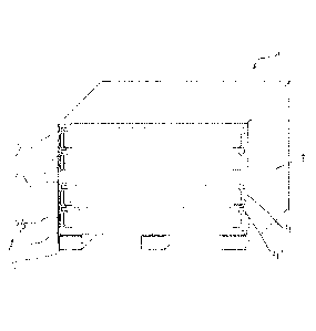
Fig. 1 shows a plurality of photovoltaic modules 1 which are arranged one on
top
of the other on a pallet 7. The photovoltaic modules 1 form a stack and are
surrounded by a stretch film 8. The photovoltaic modules 1 are protected
against
contamination during transport by the stretch film 8.
A photovoltaic module 1 consists of a frame 21 which surrounds the periphery
of
the solar cell 2 or the photovoltaic element 3. The frame 21 consists of a
plurality
of frame elements 4, 4', 4" which are suitable for being arranged one on top
of the
other. This is clear from Fig. 1, which shows that, for example, a second
frame
element 4" is located above a first frame element 4'. The frame element 4 is
profiled and has projections 12 and recesses 13 which engage in one another
when the photovoltaic modules 1 are stacked, and thus fix the individual
photovoltaic modules 1 in relation to one another.
The frame element 4 consists, for example, of a metal, plastics material, or
the like
and has a hollow chamber 5. The hollow chamber profile significantly reduces
the
weight of the frame 21. At the same time, the profiled design of the frame
element
4 allows a high level of strength to be achieved. Another advantage of the
hollow
Date Recue/Date Received 2021-05-18
7
chamber profile is that connection cables, for example, can be guided in the
hollow
space 5, which cables are thus protected against damage.
The size of the photovoltaic modules 1 substantially corresponds to the size
of a
EUR-pallet. However, other sizes are also possible.
Fig. 2 shows the photovoltaic module 1 in detail. The photovoltaic module 1
consists of the frame elements 4, which are profiled and have a receiving
portion
11 for the planar solar cell 2 or the photovoltaic element 3. The receiving
portion
11 consists of an upper receiving portion limb 12 and a lower receiving
portion
limb 13, which are arranged so as to be vertically spaced and form a U-shaped
receiving portion 11 for the planar solar cell 2 or the photovoltaic element
3.
The vertical distance between the upper receiving portion limb 12 and the
lower
receiving portion limb 13 preferably corresponds approximately to the plate
thickness of the solar cell 2 or the photovoltaic element 3. This makes it
possible
for the receiving portion 11 of the frame element 4 to be plugged onto the
solar cell
2 or the photovoltaic element 3.
There is a projection 12 in the region of the upper receiving portion limb 9.
The
dimensions of the projection 12 correspond approximately to the dimensions of
the
recess 13 which is located on the opposite side of the frame element 4. If a
first
frame element 4' is now arranged on a second frame element 4", the projection
12
of the first frame element 4' engages in the recess of the second frame
element 4".
This secures the position of the two frame elements 4' and 4' arranged one on
top
of the other or of the entire photovoltaic modules 1.
The receiving portion 11 is U-shaped, the length of the receiving portion 11
or the
upper and lower receiving portion limbs 9, 10 being such that the solar cell 2
or the
photovoltaic element 3 is held by the receiving portion 11 at least in the
edge
region, i.e., in the region of the side edge 19. The projection 12 on the
upper
receiving portion limb 9 is located in the region of the receiving portion 11,
the
recess 13 being located on the opposite side. Both the projection 12 and the
recess 13 are thus located in the edge region of the solar cell 2 or the
photovoltaic
Date Recue/Date Received 2021-05-18
8
element 3. This results in a very good load transfer between the individual
edge
elements 4, 4' and 4", because the load created by a plurality of photovoltaic
modules 1 arranged one on top of the other is almost completely transferred by
the frame elements 4, 4' and 4".
Fig. 3 shows the frame element 4 comprising the receiving portion 11 in
detail. The
receiving portion 11 is formed by the two spaced receiving portion limbs 9,
10. The
projection 12 is located on the upper side of the upper receiving portion limb
9, the
recess 13 being in alignment on the opposite side. The shape of the projection
12
and the shape of the recess 13 are such that both parts, when a plurality of
frame
elements 4, 4', 4" are stacked one on top of the other, the projection 9
engages in
the recess 10 and is held there in a form-fitting manner.
The upper side 16 of the upper receiving portion limb 9 has only round
transitions
having large radii. In particular, this avoids sharp edges or corners, which
can
cause damage when a plurality of photovoltaic modules 1 are stacked one on top
of the other.
The lower receiving portion limb 10 has a chamfer 17 at the outer point, which
is
designed as an insertion chamfer. Owing to the chamfer, the edge element 4 can
be more easily plugged onto the solar cell 2 or onto the photovoltaic element
3. In
addition, the receiving portion limb 10, in particular in the region of the
chamfer
(17), has no edges, but only surfaces having radii. As a result, the
photovoltaic
element 2 or the PV composite in the region of the receiving portion 11 is
particularly handled with care when the photovoltaic element or the PV
laminate
bends due to increased temperatures and/or due to
oscillations/vibrations/impacts.
The frame element 4 has a profile limb 14 on the bottom side, which extends
toward the center of the solar cell 2 or the photovoltaic element 3. The
profile limb
14 is preferably longer than the limbs 9, 10 of the receiving portion 11. The
profile
limb 14 on the bottom side has a gripping surface 15 for a hand. As a result,
the
entire photovoltaic module 1 can easily be lifted by hand in the edge region
without
coming into contact with the solar cell 2 or the photovoltaic element 3.
Date Recue/Date Received 2021-05-18
9
Fig. 4 shows a plan view of a plurality of elongate frame elements 4 which
abut
one another at an angle. The frame elements 4 are connected in the corner
regions by means of a miter joint 18. The end regions of the frame elements 4
preferably include an angle of 45 .
The two frame elements 4 abutting one another are fixed by a connector 6. The
connector 6' can either be placed on the frame elements 4 and connected to the
frame elements 4 by an adhesive, welding, soldering or screw connection, or
the
connector 6" is pressed into the frame elements 4 by a pressing-in process.
In the embodiment according to Fig. 4, a total of four frame elements 4 are
put
together to form a peripheral frame, each of the individual frame elements 4
being
connected by a miter joint 18 and the connector 6. The frame elements 4 can
thus
be individually plugged onto the respective side edges 19 of the solar cell 2
or the
photovoltaic element 3 and then connected thereto.
For example, two frame elements 4 can be connected to one another by pressing
in the connector 6. Subsequently, the two L-shaped frame elements 4 are placed
on the side edges 19 of the solar cell 2 or the photovoltaic element 3 and
connected by two further connectors 6.
In a further embodiment, for example, all frame elements 4 can be individually
plugged onto the side edges 19 and only then connected by the connectors 6.
Fig. 5 shows an L-shaped connector 6 which produces an interlocking connection
to the adjoining frame elements 4 by means of a pressing-in force. Pressing in
the
connector is a manufacturing method from the field of joining technology. It
allows
an interlocking connection between the connector 6 and the frame element 4
without the use of auxiliary joining means. In order to achieve a better
connection
between the connector 6 and the frame element 4, the connector 6 has numerous
lamellae 20 which engage in the material of the frame element 4.
Date Recue/Date Received 2021-05-18
10
Fig. 6 shows schematically the frame elements 4, which together form a frame
21.
The frame elements 4 are connected by the connectors 6. All frame elements 4
each have a miter joint 18 at their ends. The connectors 6 are preferably
pressed
into the profile of the frame elements 4, which results in a smooth surface on
the
outside of the frame elements 4.
Fig. 7 and 8 show a straight connector 6 which is designed to connect two
straight,
adjoining frame elements 4.
According to Fig. 7, the two adjoining frame elements 4 have a miter joint 18
and
are connected to one another by a straight connector 6. By connecting two
straight
frame elements 4 by means of a straight connector 6, a plurality of frame
elements
4 can now be arranged one behind the other on one side of the photovoltaic
element 3. As a result, the frame elements 4 can be made shorter, for example,
so
that the frame elements 4 can be mounted on the photovoltaic element 3 more
easily and quickly. In addition, by arranging a plurality of frame elements 4
one
behind the other and by connecting them by means of the straight connectors 6,
particularly long photovoltaic elements 3 can be surrounded by individual
frame
elements 4. On one side of the photovoltaic element 3, not only can two frame
elements 4 be arranged one behind the other, but a plurality of frame elements
4
are also possible. The adjoining end regions (end faces) of the frame elements
4
have either a miter joint, a straight surface or a complementary surface for
the
connection to one another.
The connectors 6 according to Fig. 7 are arranged, for example, on the side
face
of the frame element 4. However, it is also possible for the frame element 4
to
have a suitable recess in its side face for the connector 6. The connector 6
then no
longer projects beyond the periphery of the frame element 4, but is completely
received on the side face of the frame element 4. In addition, by pressing the
connector 6 into the frame element 4, a completely planar side face can also
be
achieved on the frame element 4.
Date Recue/Date Received 2021-05-18
11
Fig. 8 shows the connector 6, which is designed as a straight connector
comprising lamellae 20. Instead of the lamellae 20, the connector 6 can also
have
straight surfaces comprising recesses for, e.g., a detachable connection with
a
screw connection or rivet connection to the frame element 4
Date Recue/Date Received 2021-05-18
12
Reference sign list
1. Photovoltaic module
2. Solar cell
3. Photovoltaic element
4. Frame element
5. Hollow chamber profile
6. Connector
7. Pallet
8. Stretch film
9. Upper receiving portion limb
10. Lower receiving portion limb
11. Receiving portion
12. Projection
13. Recess
14. Profile limb
15. Gripping surface
16. Upper side of 9
17. Chamfer
18. Miter joint
19. Side edge of 2 or 3
20. Lamellae
Date Recue/Date Received 2021-05-18