Note : Les descriptions sont présentées dans la langue officielle dans laquelle elles ont été soumises.
CA 03119175 2021-05-07
WO 2020/096591
PCT/US2018/059660
1
PROTECTION OF BIOLOGICAL SYSTEMS
CROSS-REFERENCES TO RELATED APPLICATIONS
FIELD
[0001] This invention relates to electro-static discharge (ESD) protection and
more particularly relates to protection of biological systems.
BACKGROUND
[0002] Electro-static charge imbalances may be induced when an object makes
contact, or proximity, with and then separates from another object with one or
more of
the objects being electrically insulating. Electro-static charge may also be
induced by
proximity to an object or surface. Electro-static charge may also be induced
by pressure,
heating, and proximity to another charged object. The charge is then
neutralized when
the charged object comes into electrical communication with a conductive or
grounded
object. The neutralization of the charge is an event known as an electro-
static discharge
(ESD). Additionally, ESD events may be sustained by typically insulating
materials
upon exceeding a breakdown voltage of the material.
SUMMARY
[0003] An apparatus for protect a biological system from molecular damage due
to electrostatic discharge is disclosed. The apparatus includes an electrical
contact
point, a resistive element, and a connection point. The electrical contact
point is
positioned to facilitate electrical communication with the biological system.
The
resistive element is coupled to the electrical contact point. The resistive
element has an
electrical resistive value tuned to drain electrostatic charge from the
biological system
based on a contact time of the electrical contact point with the biological
system. The
connection point is coupled to the resistive element to create an electrical
potential
difference across the resistive element in response to the contact of the
electrical contact
point with the biological system
[0004] A method for protecting a biological system from electrostatic
discharge
damage is also disclosed. The method includes determining a contact time for
the
biological system at an electrical contact point. The method also includes
coupling a
resistive element to the electrical contact point. The resistive element has a
resistive
value tuned, based on the contact time, to drain electrostatic charge from the
biological
system. The method also includes coupling a connection point to the resistive
element
CA 03119175 2021-05-07
WO 2020/096591
PCT/US2018/059660
2
to create an electrical potential difference across the resistive element in
response to
contact of the biological system with the electrical contact point.
[0005] A wearable system to protect a biological system from molecular
damage due to electrostatic discharge is also disclosed. The wearable system
includes
an electrical contact point, a resistive element, a connection point, and a
tracking
system. The electrical contact point is positioned to facilitate electrical
communication
with the biological system. The resistive element is coupled to the electrical
contact
point. The resistive element has an electrical resistive value tuned to drain
electrostatic
charge from the biological system based on a contact time of the electrical
contact point
with the biological system. The connection point is coupled to the resistive
element to
create an electrical potential difference across the resistive element in
response to the
contact of the electrical contact point with the biological system. The
tracking system
tracks data corresponding to the biological system.
BRIEF DESCRIPTION OF THE DRAWINGS
[0006] In order that the advantages of the invention will be readily
understood,
a more particular description of the invention briefly described above will be
rendered
by reference to specific embodiments that are illustrated in the appended
drawings.
Understanding that these drawings depict only typical embodiments of the
invention,
and are not therefore to be considered to be limiting of its scope, the
invention will be
described and explained with additional specificity and detail through the use
of the
accompanying drawings, in which:
[0007] Figure 1 is a perspective view illustrating one embodiment of a DNA
protection system 102 in accordance with the present invention;
[0008] Figure 2 is an enlarged view illustrating one embodiment of a DNA
protective apparatus 200 local to a biological system 104 in accordance with
the present
disclosure;
[0009] Figure 3 is a diagram illustrating different environments in which
embodiments of DNA protection may be implemented in accordance with the
present
disclosure; and
[0010] Figure 4 is a flowchart diagram illustrating one embodiment of a method
400 for protecting DNA from electrostatic discharge damage in accordance with
the
present disclosure.
CA 03119175 2021-05-07
WO 2020/096591
PCT/US2018/059660
3
DETAILED DESCRIPTION
[0011] Reference throughout this specification to "one embodiment," "an
embodiment," or similar language means that a particular feature, structure,
or
characteristic described in connection with the embodiment is included in at
least one
embodiment. Thus, appearances of the phrases "in one embodiment," "in an
embodiment," and similar language throughout this specification may, but do
not
necessarily, all refer to the same embodiment, but mean "one or more but not
all
embodiments" unless expressly specified otherwise.
[0012] The terms "including," "comprising," "having," and variations thereof
mean "including but not limited to" unless expressly specified otherwise. An
enumerated listing of items does not imply that any or all of the items are
mutually
exclusive and/or mutually inclusive, unless expressly specified otherwise. The
terms
"a," "an," and "the" also refer to "one or more" unless expressly specified
otherwise.
The term "point" means a single point, multiple points, a region, or area
unless
expressly specified otherwise.
[0013] Furthermore, the described features, structures, or characteristics of
the
invention may be combined in any suitable manner in one or more embodiments.
In the
following description, numerous specific details are provided, such as
examples of
programming, software modules, user selections, network transactions, database
queries, database structures, hardware modules, hardware circuits, hardware
chips, etc.,
to provide a thorough understanding of embodiments of the invention. One
skilled in
the relevant art will recognize, however, that the invention may be practiced
without
one or more of the specific details, or with other methods, components,
materials, and
so forth. In other instances, well-known structures, materials, or operations
are not
shown or described in detail to avoid obscuring aspects of the invention.
[0014] The schematic flow chart diagrams included herein are generally set
forth as logical flow chart diagrams. As such, the depicted order and labeled
steps are
indicative of one embodiment of the presented method. Other steps and methods
may
be conceived that are equivalent in function, logic, or effect to one or more
steps, or
portions thereof, of the illustrated method. Additionally, the format and
symbols
employed are provided to explain the logical steps of the method and are
understood
not to limit the scope of the method. Although various arrow types and line
types may
be employed in the flow chart diagrams, they are understood not to limit the
scope of
the corresponding method. Indeed, some arrows or other connectors may be used
to
CA 03119175 2021-05-07
WO 2020/096591
PCT/US2018/059660
4
indicate only the logical flow of the method. For instance, an arrow may
indicate a
waiting or monitoring period of unspecified duration between enumerated steps
of the
depicted method. Additionally, the order in which a particular method occurs
may or
may not strictly adhere to the order of the corresponding steps shown.
[0015] These features and advantages of the embodiments will become more
fully apparent from the following description and appended claims or may be
learned
by the practice of embodiments as set forth hereinafter. As will be
appreciated by one
skilled in the art, aspects of the present invention may be embodied as a
system, method,
and/or computer program product. Accordingly, aspects of the present invention
may
take the form of an entirely hardware embodiment, an entirely software
embodiment
(including firmware, resident software, micro-code, etc.) or an embodiment
combining
software and hardware aspects that may all generally be referred to herein as
a "circuit,"
"module," or "system." Furthermore, aspects of the present invention may take
the form
of a computer program product embodied in one or more computer readable
medium(s)
having program code embodied thereon.
[0016] Many of the functional units described in this specification have been
labeled as modules, in order to more particularly emphasize their
implementation
independence. For example, a module may be implemented as a hardware circuit
comprising custom VLSI circuits or gate arrays, off-the-shelf semiconductors
such as
logic chips, transistors, or other discrete components. A module may also be
implemented in programmable hardware devices such as field programmable gate
arrays, programmable array logic, programmable logic devices or the like.
[0017] Modules may also be implemented in software for execution by various
types of processors. An identified module of program code may, for instance,
comprise
one or more physical or logical blocks of computer instructions which may, for
instance, be organized as an object, procedure, or function. Nevertheless, the
executables of an identified module need not be physically located together
but may
comprise disparate instructions stored in different locations which, when
joined
logically together, comprise the module and achieve the stated purpose for the
module.
[0018] Indeed, a module of program code may be a single instruction, or many
instructions, and may even be distributed over several different code
segments, among
different programs, and across several memory devices. Similarly, operational
data may
be identified and illustrated herein within modules and may be embodied in any
suitable
form and organized within any suitable type of data structure. The operational
data may
CA 03119175 2021-05-07
WO 2020/096591
PCT/US2018/059660
be collected as a single data set or may be distributed over different
locations including
over different storage devices, and may exist, at least partially, merely as
electronic
signals on a system or network. Where a module or portions of a module are
implemented in software, the program code may be stored and/or propagated on
in one
5 or more computer readable medium(s).
[0019] The computer program product may include a computer readable
storage medium (or media) having computer readable program instructions
thereon for
causing a processor to carry out aspects of the present invention.
[0020] The computer readable storage medium can be a tangible device that can
retain and store instructions for use by an instruction execution device. The
computer
readable storage medium may be, for example, but is not limited to, an
electronic
storage device, a magnetic storage device, an optical storage device, an
electromagnetic
storage device, a semiconductor storage device, or any suitable combination of
the
foregoing.
[0021] A non-exhaustive list of more specific examples of the computer
readable storage medium includes the following: a portable computer diskette,
a hard
disk, a random access memory ("RAM"), a read-only memory ("ROM"), an erasable
programmable read-only memory ("EPROM" or Flash memory), a static random
access memory ("SRAM"), a portable compact disc read-only memory ("CD-ROM"),
a digital versatile disk ("DVD"), a memory stick, a floppy disk, a
mechanically encoded
device such as punch-cards or raised structures in a groove having
instructions recorded
thereon, and any suitable combination of the foregoing. A computer readable
storage
medium, as used herein, is not to be construed as being transitory signals per
se, such
as radio waves or other freely propagating electromagnetic waves,
electromagnetic
waves propagating through a waveguide or other transmission media (e.g., light
pulses
passing through a fiber-optic cable), or electrical signals transmitted
through a wire.
[0022] Computer readable program instructions described herein can be
downloaded to respective computing/processing devices from a computer readable
storage medium or to an external computer or external storage device via a
network,
for example, the Internet, a local area network, a wide area network and/or a
wireless
network. The network may comprise copper transmission cables, optical
transmission
fibers, wireless transmission, routers, firewalls, switches, gateway computers
and/or
edge servers. A network adapter card or network interface in each
computing/processing device receives computer readable program instructions
from the
CA 03119175 2021-05-07
WO 2020/096591
PCT/US2018/059660
6
network and forwards the computer readable program instructions for storage in
a
computer readable storage medium within the respective computing/processing
device.
[0023] Computer readable program instructions for carrying out operations of
the present invention may be assembler instructions, instruction-set-
architecture (ISA)
instructions, machine instructions, machine dependent instructions, microcode,
firmware instructions, state-setting data, or either source code or object
code written in
any combination of one or more programming languages, including an object
oriented
programming language such as Smalltalk, C++ or the like, and conventional
procedural
programming languages, such as the "C" programming language or similar
programming languages.
[0024] The computer readable program instructions may execute entirely on the
user's computer, partly on the user's computer, as a stand-alone software
package, partly
on the user's computer and partly on a remote computer or entirely on the
remote
computer or server. In the latter scenario, the remote computer may be
connected to the
user's computer through any type of network, including a local area network
(LAN) or
a wide area network (WAN), or the connection may be made to an external
computer
(for example, through the Internet using an Internet Service Provider). In
some
embodiments, electronic circuitry including, for example, programmable logic
circuitry, field-programmable gate arrays (FPGA), or programmable logic arrays
(PLA)
may execute the computer readable program instructions by utilizing state
information
of the computer readable program instructions to personalize the electronic
circuitry, in
order to perform aspects of the present invention.
[0025] Aspects of the present invention are described herein with reference to
flowchart illustrations and/or block diagrams of methods, apparatus (systems),
and
computer program products according to embodiments of the invention. It will
be
understood that each block of the flowchart illustrations and/or block
diagrams, and
combinations of blocks in the flowchart illustrations and/or block diagrams,
can be
implemented by computer readable program instructions.
[0026] These computer readable program instructions may be provided to a
processor of a general-purpose computer, special purpose computer, or other
programmable data processing apparatus to produce a machine, such that the
instructions, which execute via the processor of the computer or other
programmable
data processing apparatus, create means for implementing the functions/acts
specified
in the flowchart and/or block diagram block or blocks. These computer readable
CA 03119175 2021-05-07
WO 2020/096591
PCT/US2018/059660
7
program instructions may also be stored in a computer readable storage medium
that
can direct a computer, a programmable data processing apparatus, and/or other
devices
to function in a particular manner, such that the computer readable storage
medium
having instructions stored therein comprises an article of manufacture
including
instructions which implement aspects of the function/act specified in the
flowchart
and/or block diagram block or blocks.
[0027] The computer readable program instructions may also be loaded onto a
computer, other programmable data processing apparatus, or other device to
cause a
series of operational steps to be performed on the computer, other
programmable
apparatus or other device to produce a computer implemented process, such that
the
instructions which execute on the computer, other programmable apparatus, or
other
device implement the functions/acts specified in the flowchart and/or block
diagram
block or blocks.
[0028] Many of the functional units described in this specification have been
.. labeled as modules, in order to more particularly emphasize their
implementation
independence. For example, a module may be implemented as a hardware circuit
comprising custom VLSI circuits or gate arrays, off-the-shelf semiconductors
such as
logic chips, transistors, or other discrete components. A module may also be
implemented in programmable hardware devices such as field programmable gate
arrays, programmable array logic, programmable logic devices or the like.
[0029] Modules may also be implemented in software for execution by various
types of processors. An identified module of program instructions may, for
instance,
comprise one or more physical or logical blocks of computer instructions which
may,
for instance, be organized as an object, procedure, or function. Nevertheless,
the
executables of an identified module need not be physically located together
but may
comprise disparate instructions stored in different locations which, when
joined
logically together, comprise the module and achieve the stated purpose for the
module.
[0030] The schematic flowchart diagrams and/or schematic block diagrams in
the Figures illustrate the architecture, functionality, and operation of
possible
.. implementations of apparatuses, systems, methods, and computer program
products
according to various embodiments of the present invention. In this regard,
each block
in the schematic flowchart diagrams and/or schematic block diagrams may
represent a
module, segment, or portion of code, which comprises one or more executable
instructions of the program code for implementing the specified logical
function(s).
CA 03119175 2021-05-07
WO 2020/096591
PCT/US2018/059660
8
[0031] It should also be noted that, in some alternative implementations, the
functions noted in the block may occur out of the order noted in the Figures.
For
example, two blocks shown in succession may, in fact, be executed
substantially
concurrently, or the blocks may sometimes be executed in the reverse order,
depending
upon the functionality involved. Other steps and methods may be conceived that
are
equivalent in function, logic, or effect to one or more blocks, or portions
thereof, of the
illustrated Figures.
[0032] Although various arrow types and line types may be employed in the
flowchart and/or block diagrams, they are understood not to limit the scope of
the
corresponding embodiments. Indeed, some arrows or other connectors may be used
to
indicate only the logical flow of the depicted embodiment. For instance, an
arrow may
indicate a waiting or monitoring period of unspecified duration between
enumerated
steps of the depicted embodiment. It will also be noted that each block of the
block
diagrams and/or flowchart diagrams, and combinations of blocks in the block
diagrams
and/or flowchart diagrams, can be implemented by special purpose hardware-
based
systems that perform the specified functions or acts, or combinations of
special purpose
hardware and program code.
[0033] ESD events have been recognized as destructive for sensitive electronic
microcircuits but, until now, little has been understood about the effect on
biological
systems. The energy contained in a single ESD event is known to reach
relatively high
and potentially destructive levels. For example, ESD events may reach 15,000
volts,
25,000 volts, 50,000 volts, or more with a current of 30 amperes or greater.
Such levels
are considered fatal in a sustained event. It is due to the relatively brief
period of time
in which these events occur that common ESD events are not fatal. However, the
level
of energy involved in a common ESD events is above levels capable of causing
cellular
and molecular damage to biological systems.
[0034] A single ultraviolet (UV) photon is known to affect damage on
deoxyribonucleic acids (DNA) resulting in mutations that can lead to cancers.
The
energy of the average UV photon is orders of magnitude less than that of the
average
ESD event. Therefore, the energy contained in each ESD event is more than
sufficient
to cause fundamental damage to DNA. While most damage is repaired by enzymes,
with frequent and repeated damage, the chance of persistent damage increases.
As ESD
events are common and occur in a wide range of situations in daily life, the
risk of DNA
damage due to ESD is considerable.
CA 03119175 2021-05-07
WO 2020/096591
PCT/US2018/059660
9
[0035] The human body may be approximately modeled as a capacitor. The
energy of a capacitor may be represented mathematically as E = 1/2CV2 where E
=
energy, C = capacitance, and V = voltage. Because voltage (V) is a squared
term in the
equation, decreasing the voltage in a human body model results in a large
reduction in
the energy involved in the system. The term "human body model" refers to a
circuit
diagram with a behavior approximating or simulating a human body.
[0036] Further, because the behavior of a capacitor, and the human body, is
asymptotic in nature, the energy never truly reaches zero. Solutions provided
herein
seek to optimize available contact time to shunt charge in a safe manner to
avoid
biological damage. For example, mitochondrial and nuclear DNA damage and
damage
to other cellular components and system due to ESD events are prevented or
significantly reduced.
[0037] Described herein are methods, systems, and apparatuses which have a
tuned resistance value based on an expected time of contact. Embodiments
described
herein may have a resistive value tuned to draw down the charge built up on a
biological
system. The amount the charge is drawn down may be the total charge amount or
a
portion of the total charge. In some embodiments, the tuning may also be based
on a
frequency of touches as well as a material involved in each touch. For
example, a
system with more frequent touches with the biological system may have a higher
resistance to draw off less charge to lower the amount of energy applied to
the DNA
with each draw-down. The higher frequency of touches would allow for draw-
downs
to occur more often which would keep the charge of a biological system at safe
levels
and reduce damage from discharges.
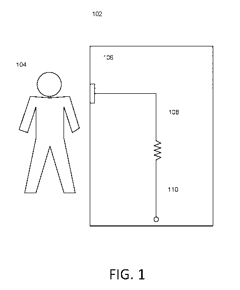
[0038] Figure 1 is a perspective view illustrating one embodiment of a DNA
protection system 102 in accordance with the present invention. In the
illustrated
embodiment, the DNA protective system 102 is remote to a biological system
104. In
the illustrated embodiment, the biological system 104 is a person. In other
embodiments, the biological system 104 is a non-human system. In the
illustrated
embodiment, the DNA protection system 102 includes a contact point 106, a
resistive
element 108, and a connection point 110.
[0039] In some embodiments, the contact point 106 is an electrical contact
point. In some embodiments, the contact point 106 is at least partially
electrically
conductive. In some embodiments, the contact point 106 is a stand-alone
component.
For example, the contact point 106 may be coupled to but separate from the
rest of the
CA 03119175 2021-05-07
WO 2020/096591
PCT/US2018/059660
DNA protection system 102. In other embodiments, the contact point 106 is
integrated
with a surface or structure of another component or system.
[0040] In some embodiments of the DNA protective system, grounded
conductive elements capable of sustaining an ESD event may be insulated to
prevent
5 untuned
discharge. For example, metal screws may be replaced with tuned shunting
screws or insulated components, facias and other body panels of different
systems may
be swapped for tuned or insulating equivalents. Some metallic components may
not be
grounded but still facilitate an ESD event (door knob, light switch plate,
etc.). DNA
protection systems may be put in place which equalize the charge across the
user and
10 environmental component without causing an ESD event.
[0041] In some cases, conductive elements may not be fully insulated. In these
situations, additional shunting considerations or calculations may be employed
as
protection. In one example, an ESD event may occur on a bedsheet as a sleeper
moves
around in the bed. A tuned charge shunt path may drain off the charge as it is
generated
and reduce the chance of an ESD event. In another example, when two people are
sleeping in a single bed, tuned shunting paths may be formed in bedding,
clothing, and
other components to constantly or periodically shunt charge to prevent a
mutual ESD
event between the sleepers and ESD events between a sleeper and other points
of
contact such as an alarm clock, bedframe, bedside lamp, light switch, and the
like.
[0042] The resistive element 108 is electrically coupled to the contact point
106.
The resistive element 108 may be a fixed or variable resistive component. For
example,
the resistive element 108 may be manually or automatically adjustable. In some
embodiments, the resistive element 108 is coupled to a sensor or other
component
which adjusts the resistivity of the resistive element 108 based on a detected
condition.
For example, a detected charge on a biological system 104 at or near the
contact point
106 may allow the resistive element 108 to be tuned to a corresponding
resistivity.
[0043] In the illustrated embodiment, the resistive element 108 is a separate
component from the contact point 106. In some embodiments, the resistive
element 108
is integrated with the contact point 106. For example, the resistive element
108 may be
a material that makes up at least a portion of the contact point 106 or a
component
integrated into or coupled to the contact point 106.
[0044] In some embodiments, the resistive element 108 has a bulk resistance in
the giga-ohm range. In other embodiments, the resistive element 108 has a bulk
resistance that is magnitudes higher or lower than the giga-ohm range. The
resistance
CA 03119175 2021-05-07
WO 2020/096591
PCT/US2018/059660
11
value of the resistive element 108 may be tuned to correspond to a time of
contact
between the biological system 104 and the contact point 106.
[0045] The resistive element 108 may also be tuned based on the intrinsic
material properties of the materials involved in the charge path. For example,
the
resistance of the DNA protection system 102 may be tuned based on an expected
contact time. The contact time may be less than five seconds, less than one
second, or
a few milliseconds. In some embodiments, the resistive element 108 is tuned to
correspond to five time-constants. Other embodiments may be tuned to few or
more
than five time-constants.
[0046] In some embodiments, the resistive value of the resistive element 108
is
determined based on a factor applied to a time-constant for the material or
object
involved as well as the desired percentage or amount of charge to shunt or
drain during
the period of contact between the biological system 104 and the electrical
contact point
106.
[0047] In some embodiments, the resistive element 108 is coupled to the
connection point 110. The connection point 110 may be a fixed or mobile
ground. The
connection point 110 may form a circuit ground or earth ground. The connection
point
110 may be part of an energy storage system or a true ground.
[0048] In some embodiments, the connection point 110 is not a true ground but
representative of the other side of a potential ESD event. For example, if a
person is
exiting an automobile after building up a significant amount of charge with
respect to
the automobile, a tuned DNA protective system 102 may shunt the charge between
the
person and the automobile during the exit at a rate that is slow enough, and
to a voltage
level low enough, to avoid an ESD event. Because the automobile is on
insulating
rubber tires, no true ground is present in the system. As described above, the
rate of the
charge transfer should be tuned such that the transfer does not reach a rate
which could
potential damage DNA.
[0049] Figure 2 is an enlarged view illustrating one embodiment of a DNA
protective apparatus 200 local to a biological system 104 in accordance with
the present
disclosure. In the illustrated embodiment, the DNA protective apparatus 200 is
proximal the biological system 104. In some embodiments, the DNA protective
apparatus 200 is small relative to the biological system 104. The DNA
protective
apparatus 200 may be contained, as shown, in a single unit or separated into
two or
more units.
CA 03119175 2021-05-07
WO 2020/096591
PCT/US2018/059660
12
[0050] One or more of the components of the DNA protective apparatus 200
may be as described above with respect to Figure 1. For example, one or more
of the
contact point 106 and the resistive element 108 may be configured or tuned for
an
expected duration of contact, by the biological system 104, at the contact
point 106. In
some embodiments, the DNA protective apparatus 200 is in frequent contact with
the
biological system 104.
[0051] In other embodiments, the DNA protective apparatus 200 is in
infrequent contact with the biological system 104. In some embodiments, the
DNA
protective apparatus 200 initiates a charge drain or shunting. The shunting
may be
initiated via actuation of some component of the DNA protective apparatus 200
to cause
contact or complete a circuit with the biological system. Shunting may also be
initiated
by providing a notification or alert to provide contact with the DNA
protective
apparatus 200. In other embodiment, the DNA protective apparatus 200 is
passive in
that the DNA protective apparatus 200 may shunt charge in response to contact
or other
input from the biological system 104 without the DNA protective apparatus 200
executing processes to initiate the shunting.
[0052] In some embodiments, the DNA protective apparatus 200 is associated
with a single biological system 104. In other embodiments, the DNA protective
apparatus 200 is associated with a plurality of biological systems 104. For
example, the
DNA protective apparatus 200 may be a personal device or a public or common
device.
In some embodiments, the DNA protective apparatus 200 is a satellite unit that
is
associated with a base unit. In other embodiments, the DNA protective
apparatus 200
is a stand-alone unit.
[0053] Figure 3 is a diagram illustrating different environments in which
embodiments of DNA protection may be implemented in accordance with the
present
disclosure. The illustrated embodiment includes a domicile environment 300.
The
domicile environment 300 may include a home, hotel, dormitory, or other
residential
or commercial domicile. The illustrated embodiment also includes an
occupational
environment 302. The occupational environment 302 may include an office, shop,
meeting place, restaurant, store, or the like.
[0054] Each of the domicile environment 300 and the occupational
environment 302 may DNA protective systems 102 or apparatuses 200. In these
environments 300 and 302, the DNA protective systems 102 may be placed or
integrated into human interfaces or other systems which are contacted by a
biological
CA 03119175 2021-05-07
WO 2020/096591
PCT/US2018/059660
13
system 104. For example, the protective systems 102 may include one or more of
carpeting, rugs, tile, laminate, wood, and other flooring or floor coverings,
light
switches, doors, door plates, door handles, hand rails, faucets, toilets,
furniture such as
beds and bedding/sheets, tables, chairs, desks, elevators, elevator call
buttons, stairs and
stair coverings, shopping carts and bags, registers, shelves, displays,
keypads, pens,
styluses, keyboards (and keyboard keys), mice, touchpads, computers such as
laptops,
tablets, and desktops, and other known systems, structures, and the like.
[0055] Figure 3 also includes a transportation environment 304. The
transportation environment 304 may include a can, bus, train, boat, plane, and
the like.
Embodiments described herein may be incorporated into human interfaces or
other
systems and structures of the transportation environment 304 which comes into
contact
with a biological system 104. For example, the DNA protective system 104 may
include
one or more of doors, door handles, door knobs, door panels, keypads, key
slots,
kickplates, vehicle body panels, vehicle interior panels, steering wheels or
other control
interfaces such as parking breaks, shift handles, pedals, stereo and other
entertainment
controls, and climate controls, and the like, seats, flooring, consoles,
dashes, seatbelts,
seatbelt receivers, and other known systems, structures, and the like.
[0056] The illustrated embodiment of Figure 3 also includes a personal
environment 306. The personal environment 306 may include clothing. For
example,
socks, shoes, and other footwear may be effective. The personal environment
306 may
also include accessories such as jewelry, belts, hats, purses, wallets,
keychains, glasses,
and the like. The personal environment 306 may also include personal devices
such as
phones, tablets, watches, music players, headphones, and the like.
[0057] In some embodiments, the personal devices may track electrostatic
buildup on the biological system 104 and provide a warning or alert in
response to the
electrostatic buildup reaching unsafe levels. The personal device may prompt a
discharge or provide other instructions to facilitate safe and non-damaging
charge
shunting. Additionally, the personal device or other systems may track charge
levels,
ESD events, and the like and provide records or data in a feedback loop to the
user to
modify behavior, address potential hazards, or the like.
[0058] In some embodiments, one or more of the components of the
environments 300, 302, 304, and 306 cooperate to drain or shunt electrostatic
charge
from a biological system 104 at a rate that reduces the chance of damage to
DNA of the
biological system 104 due to electrostatic discharge events. For example,
shoes may be
CA 03119175 2021-05-07
WO 2020/096591
PCT/US2018/059660
14
tuned to work in tandem, as a system, with tuned carpets or other flooring
surfaces/materials.
[0059] While some embodiments incorporate DNA protective systems 102 and
apparatuses 104 into existing components, other embodiments provide DNA
protective
systems 102 and apparatuses 104 as standalone components which may be hidden
or
openly identifiable. In some embodiments, a presence of the DNA protective
systems
102 and apparatuses 104 may be masked or hidden to preserve aesthetic
characteristic
of the corresponding structure. In other embodiments, the presence of the DNA
protective systems 102 and apparatuses 104 may be emphasized or highlighted to
prompts contact or use of the DNA protective systems 102 and apparatuses 104.
[0060] Figure 4 is a flowchart diagram illustrating one embodiment of a method
400 for protecting DNA from electrostatic discharge damage in accordance with
the
present disclosure. In the illustrated embodiment, the method 400 includes
determining
402 a contact time for a biological system at an electrical contact point. The
method
400 also includes coupling 404 a resistive element to the electrical contact
point, the
resistive element having a resistive value tuned, based on the contact time,
to drain
electrostatic charge from the biological system. The method 400 also includes
coupling
406 a connection point to the resistive element to create an electrical
potential
difference across the resistive element in response to contact of the
biological system
with the electrical contact point.
[0061] The present invention may be embodied in other specific forms without
departing from its spirit or essential characteristics. The described
embodiments are to
be considered in all respects only as illustrative and not restrictive. The
scope of the
invention is, therefore, indicated by the appended claims rather than by the
foregoing
description. All changes which come within the meaning and range of
equivalency of
the claims are to be embraced within their scope.