Note : Les descriptions sont présentées dans la langue officielle dans laquelle elles ont été soumises.
CA 03120784 2021-05-20
WO 2020/106855 PCT/US2019/062433
1
ELECTRO MAGNETIC REFRESHABLE BRAILLE READER
CROSS-REFERENCE TO RELATED APPLICATIONS
This application claims the benefit of U.S. Provisional Application No.
62/769,680 filed on November 20, 2018, which is hereby incorporated by
reference in its entirety.
BACKGROUND
Although several different technologies have been explored for the
creation of tactile displays, none have been suitable to produce a full page
tactile
display. Such a display requires high-density and power efficient actuation
devices. Therefore, there remains a need for improvement in this field.
SUMMARY
Various embodiments of tactile displays are disclosed. In certain
embodiments an electromagnetic actuator may be used to control raising and
lowering of tactile elements, such as dots, and/or braille characters.
In one embodiment the present disclosure, a tactile display can be
manufactured with two enclosures removably joined together-one housing the
tactile elements will be second houses the actuation mechanisms, so that the
top
enclosure can be removed and cleaned by the user.
In one embodiment, the circuitry of a tactile display of the present
disclosure can be made to minimize the number of signals required to actuate
the high density array, minimizing leakage current and the thermal output of
the components. The circuitry can be made physically compact and relatively
inexpensive.
In some embodiments, input may be obtained by a user using tactile
displays of the present disclosure. In certain embodiments, buttons, switches,
keys, or other input devices may be used to interact with tactile displays.
Additional embodiments of the invention, as well as features and
advantages thereof, will be apparent from the descriptions herein.
CA 03120784 2021-05-20
WO 2020/106855 PCT/US2019/062433
2
BRIEF DESCRIPTION OF THE DRAWINGS
Fig. 1 shows a digital image of one example of a conventional piezoelectric
braille cell.
Fig. 2 shows a digital image of a rendering of an engineering diagram mid-
sized EMBR prototype.
Fig. 3 shows the midsize EMBR prototype of figure 2 with a touchscreen.
Fig. 4 shows a digital image of a small EMBR prototype.
Fig. 5 shows a close-up digital image of the small EMBR prototype of Fig.
4.
Fig. 6 shows a digital image of a rendering of an engineering diagram of a
large EMBR device.
Fig. 7 shows a side view digital image of a rendering of an engineering
diagram of a large EMBR device.
Fig. 8 shows an overview drawing of the side view of an EMBR cell.
Fig. 9 shows a drawing of a side view of an EMBR bottom assembly.
Fig. 10 shows a drawing of a side view of an EMBR middle assembly.
Fig. 11 shows a drawing of a side view of an EMBR middle assembly.
Fig. 12 shows a drawing of an EMBR top assembly.
Fig. 13 shows a drawing of a Braille display actuator with energetics.
Fig. 14 shows a diagram of a Braille display actuator energetics.
Fig. 15 shows a drawing of a Braille display middle assembly.
Fig. 16 shows a side view cutout digital image of a rendering of an EMBR
display.
Fig. 17 shows a drawing of a coil used in embodiments of the present
disclosure.
Fig. 18 shows a digital image of a fully wound coil around a bobbin with
leads attached to metal posts.
Fig. 19 shows a drawing of a coil cup used in embodiments of the present
disclosure.
CA 03120784 2021-05-20
WO 2020/106855 PCT/US2019/062433
3
Fig. 20 shows a digital image of a coil cup used in embodiments of the
present disclosure.
Fig. 2 1shows a drawing of a coil pack assembly as used to form one unit of
a Braille cell.
Fig. 22 shows a digital image of the front view of an open coil assembly
machine.
Fig. 23 shows a digital image of the front view of a closed coil assembly
machine.
Fig. 24 shows a digital imaging of a simulation of a shielding assembly
coupled to a coil magnetic assembly as viewed from the side.
Fig. 25 shows an underside of a top core plate comprising four Braille cells
as used in some embodiments of the present disclosure.
Fig. 26 shows a top surface of a top core plate comprising four Braille cells
as used in some embodiments of the present disclosure showing chamfered holes.
Fig. 27 shows a drawing of the top front view of a bottom core plate.
Fig. 28 shows a drawing of the top view of a plastic spacer with magnet
and coil wire holes.
Fig. 29 shows a drawing of the bottom view of a plastic spacer with
magnet, coil wire, colloidal lead, and bottom core plate holes.
Fig. 30 shows a digital image of the top view of an assembled plastic
spacer and bottom core plate.
Fig. 31 shows a digital image of the bottom view of an assembled plastic
spacer and bottom core plate.
Fig. 32 shows a digital image of the side view of an assembled plastic
spacer and bottom core plate.
Fig. 33 shows a digital image of an exploded view of a rendering of one
embodiment of the present disclosure showing the top and bottom capture plate
with pins.
Fig. 34 shows a drawing of a Braille dot pin as used in some embodiments
of the present disclosure.
CA 03120784 2021-05-20
WO 2020/106855 PCT/US2019/062433
4
Fig. 35 shows a drawing of the side view of one embodiment of the present
disclosure including a removable top half of a braille dot assembly, which can
be
removed for cleaning.
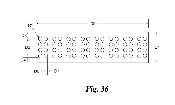
Fig. 36 shows a drawing of one embodiment of the present disclosure
including the spacing dimensions of one line of one row of cells of Braille
characters.
Fig. 37 shows one embodiment of the present disclosure using hexagonal
closest packed dots.
Fig. 38 shows a digital image of a oscilloscope with data showing the
velocity of a magnet versus time with when no sound dampening is used.
Fig. 39 shows a digital image of oscilloscope data showing the velocity of a
magnet versus time at top impact with sound dampening used.
Fig. 40 shows a digital image of oscilloscope data showing the velocity of a
magnet versus time at bottom impact with sound dampening used.
Fig. 41 shows just a digital image of the wave form obtained during audio
testing of sound dampening in one embodiment of the present disclosure.
Fig. 42 shows a drawing showing the use of sound dampening material
inside the shaft of a braille dot pin of one embodiment of the present
disclosure.
Fig. 43 shows a summary of the sound testing before sound dampening
material was added.
Fig. 44 shows a summary of the sound testing after sound dampening
material was added.
Fig. 45 shows a drawing of one embodiment of the present disclosure
which uses a PCP as the top plate which allows for touch sensitive traces as
used
in some embodiments of the present disclosure.
Fig. 46 shows a drawing of the side view of one embodiment of the present
disclosure.
Fig. 47 shows a drawing of the side view of one embodiment of the present
disclosure.
Fig. 48 shows a digital image of a rendering of one embodiment of the
present disclosure with control buttons.
CA 03120784 2021-05-20
WO 2020/106855 PCT/US2019/062433
DETAILED DESCRIPTION
For the purposes of promoting an understanding of the principles of the
invention, reference will now be made to certain embodiments and specific
language will be used to describe the same. It will nevertheless be understood
5 that no limitation of the scope of the invention is thereby intended, such
alterations and further modifications, and such further applications of the
principles of the invention as described herein being contemplated as would
normally occur to one skilled in the art to which the invention relates.
Additionally, in the detailed description below, numerous alternatives are
given
for various features. It will be understood that each such disclosed
alternative,
or combinations of such alternatives, can be combined with the more
generalized
features discussed in the Summary above, or set forth in the embodiments
described below to provide additional disclosed embodiments herein.
The electromagnetic braille readers (EMBR) of the present disclosure
represents an improvement and a new innovation in the field of tactile and
braille displays. Several variations of the disclosed embodiments has been
developed. Braille readers of the past often used piezoelectric actuators to
move
the tactile elements. These piezoelectric actuators are relatively expensive,
fragile, slow to change states, require unsafe voltages to actuate, and are
relatively large. These disadvantages severely limit the number of movable
tactile elements that can be displayed on a device using piezoelectric
technology.
Additionally these devices which use piezoelectric technology require
maintenance in the form of regular cleaning of the display elements to
maintain
the functionality of the units. Such cleaning is often performed by
technicians in
the field and is therefore time-consuming and expensive.
Although several different technologies have been explored for the
creation of tactile displays there remains a need for improvement in the art
these such displays require high density and power efficient actuating
devices.
Furthermore, to be commercially successful, the mechanism may preferentially
be relatively inexpensive.
CA 03120784 2021-05-20
WO 2020/106855 PCT/US2019/062433
6
The actuation mechanisms used in embodiments of the present disclosure
include a permanent magnet for latching. The mechanisms also include a coil
adjacent to the permanent magnet. When a current flows through the coil, the
position of the permanent magnet can be altered between two positions. In this
way, the permanent magnet can be associated with a tactile element or a
braille
dot. This position can be altered depending on the position of the permanent
magnet. When a permanent magnet is stationary in either of the two positions,
no current need be applied to the coil to maintain the position of the magnet,
substantially illuminating idle power draw. Utilizing this unique actuation
mechanism, a high-density tactile display can be made inexpensively and of
virtually unlimited size, with minimum power use.
In some embodiments of the present disclosure a tactile display can be
manufactured with two enclosures that can be removably joined together to form
the tactical display. One of these enclosures can house the tactile elements
while
the second enclosure can hold the actuation mechanism. The first enclosure can
be made suitably to be cleaned by the user themselves when removed from the
second enclosure and rejoined to the second enclosure when the cleaning is
complete.
The circuitry for the operation of the actuation mechanism can support a
high-density array of actuating devices. For example, the circuitry can be
made
to minimize the number of signals required to actuate the array, to minimize
the
leakage current of the circuitry components, and/or to minimize the thermal
output of the circuitry components. Additionally, the circuitry can be made
physically compacts to support the high-density array and can be made
relatively inexpensively.
Devices of the present disclosure may be interactive. Devices of the
present disclosure may allow a users to input content and to manipulate
displayed information. Therefore, the user can interact with the displayed
information. These devices and can include both tactile output and input in
the
form of buttons, controls, and user interface.
CA 03120784 2021-05-20
WO 2020/106855 PCT/US2019/062433
7
Devices of the present disclosure are interoperable. The devices can
interoperate with other information and communications technology (ICT)
devices, including other assistive technologies available on the market. For
example, devices of the present disclosure VFO-compatible, and can work
seamlessly with JAWS (Job Access With Speech).
Devices of the present disclosure support back translation. This allows for
the back translation of braille or tactile graphics into text or images.
Devices of the present disclosure are ready. Devices have met technology
readiness level (TRL) seven (TRL-7), meaning that system prototypes have been
demonstrated in an operational environment.
There is a need among braille literature users for display that is
affordable, and capable of displaying both text and graphics in real time.
Such
displays may preferably be of significant size, such as the size of a consumer
tablet or greater. Further, displays may preferably be able to interconnect
with
consumer computers and electronics to show graphical and braille text
representations of content. Braille literacy requires full access to content,
much
of which is graphical or two-dimensional in nature, such as tables or
formatted
braille. Existing one line displays currently on the market cannot act purely
capture such content.
Figure 1 shows a digital image of the conventional piezoelectric braille cell
technology. The basic mechanism of the piezoelectric actuator is a bimorph
which requires a long, lever like horizontal component in order to accomplish
the
correct vertical motion of an individual dot. Hence, the full actuator is much
longer than the dot itself. Although some improvements in size and packaging
have been made over the past 20+ years, the basic technology and size
limitation
remains the same. This prevents dots from being closely packed together. The
best that could previously be accomplished is two lines of braille, with a
significant bezel around them to allow for the horizontal levers. To overcome
this
size limitation and actuator which is the physical size of the dot itself is
most
desirable.
CA 03120784 2021-05-20
WO 2020/106855 PCT/US2019/062433
8
The cost factor is also a major limitation of piezoelectric technology. Again,
improvements have been made, but the basic cost is on the order of
approximately $15 US per braille cell. This is a fundamental limitation for
making larger displays. A "full-page" display may be composed of 32 cells
arranged in 16 closely packed lines similar to a braille page. Such a page
represents 512 cells, or a cost of $7680 just for the cells alone when made
with
piezoelectric technology cells. To be feasible, a new technology should cost
roughly an order of magnitude less; for example, a cost of approximately $1.50
US per braille cell may be desirable and may allow for full-page displays to
be
sold at roughly the same price as current conventional one line displays.
Devices of the present disclosure overcome many of these limitations as
well as affording multiple other improvements over conventional technologies.
The actuation mechanism used in embodiments of the present disclosure
includes a permanent magnet for latching. The mechanism also includes a coil
adjacent to the permanent magnet. When current flows through the coil, the
position of the permanent magnet can be altered between two positions. In this
way, the permanent magnet can be associated with a tactile element or a
braille
dot whose position can be altered depending on the position of the permanent
magnet. When the permanent magnet is stationary in either of the two
positions,
no current need he applied to the coil to maintain the position of the magnet,
substantially eliminating idle power draw. Utilizing this unique actuation
mechanism, a high-density tactile display can be made inexpensively of
virtually
unlimited size, with minimum power use.
One feature of tactile displays of the present disclosure includes the
feature that such tactile displays can be manufactured with two enclosures
that
can be removably joined together to form the tactile display. One of these
enclosures can house the tactile elements, while the second enclosure can
house
the actuation mechanism. The first enclosure can be made suitably to be
cleaned
by the user themselves when removed from the second enclosure and can be
rejoined to the second enclosure when the cleaning is complete.
CA 03120784 2021-05-20
WO 2020/106855 PCT/US2019/062433
9
Figure 2 shows a digital image of an engineering diagram of one mid sized
prototype of the present disclosure. Figure 3 shows a digital image of an
engineering drawing of one mid sized prototype of the present disclosure with
a
touchscreen. Figure 4 shows a digital image of one embodiment of a prototype
of
the present disclosure. Figure 5 shows a digital image of one embodiment of a
prototype of the present disclosure. Figure 6 shows a digital image of one
embodiment of a larger device of the present disclosure. Figure 7 shows a
digital
image of a side view of a larger device of the present disclosure.
Devices of the present disclosure exist in an arena that is not common for
conventional manufacturing. Many technologies exist for the manufacture of
large parts, or parts that exist on the centimeter scale or larger. Further,
modern
manufacturing technique for microelectromechanical systems (MEMS) are
becoming more common as well. However the problem of displaying braille dots
exists in the realm of millielectromechanical systems (MiMEMS), which is an
area that very few conventional manufacturers have been able to work in. In
recent years, the ability of manufacturers such as injection molding
companies,
sheet metal companies, soldering and/or printed circuit boards (PCB) has
improved.
The sheer number of parts involved in a full-page braille display is
significant. A full-page braille display can consist of tens of thousands of
individual parts on the bill of materials, similar in magnitude to a luxury
automobile. In order for manufacturing to be practical at a cost less than
that of
a luxury automobile, significant attention must be given to the use of the
conventional, well understood, and inexpensive manufacturing techniques along
with the use of inexpensive materials.
Table 1 shows a comparison between the use of a conventional piezo cell
and the electromagnetic actuators of the present disclosure.
CA 03120784 2021-05-20
WO 2020/106855 PCT/US2019/062433
Comparison Point Convention Piezo Cell EMBR Actuator
Footprint Single line only due to Supports full-page and
geometry of actuator graphic array
Cost Upwards of $15 US per Target cost $2-$4 US per
cell cell
Response time 30 ms entire display (1 200 to 800 ms for entire
line) display (page)
Dot Height 0.787 mm 0.787 mm with tighter
tolerance. Can be set
higher.
Dot Force 14-23 g 20-25 g, but with
resistance to feel firmer.
Can be set much higher
or somewhat lower.
Manufacturability Dedicated supplier Manufacturable
dependencies; high anywhere; uses tried and
production maintenance true methods
Reliability Requires regular Extremely robust
maintenance
Noise level Low to acceptable Similar in tests;
acceptable at the very
least
Power requirements 98 mj to change state for 10 - 20 mj per dot state
40 cells, plus leakage change but no holding
when holding state. Does power required. Entire
not hold state when display is very power
powered off. efficient.
Tactile displays of the present disclosure are preferably easy to read,
understand, perceive, and/or operate. The displays of the present disclosure
are
also usable, allowing users to access digital information in an effective and
CA 03120784 2021-05-20
WO 2020/106855 PCT/US2019/062433
11
timely way. The time it takes for the displays of the present disclosure to
update
and present new content do not represent a significant disruption to the user.
The adequacy of the refresh speed may depend on the chosen application for the
tactile device, with some applications requiring a higher refresh speed than
.. others. The displays of the present disclosure allow for a quiet operation
of the
display and may help to avoid discrimination when using the device in public
spaces. It enables people with visual impairments to meet their goals with
effectiveness, efficiency, and satisfaction. The devices of the present
disclosure
are also affordable and portable. Displays of the present disclosure have a
considerate design, are reliable, robust, and/or safe. They take into account
the
needs and preferences of visually impaired people. The designs of tactile
displays
of the present disclosure are aesthetically pleasing, and include practical
details
such as the format and location of navigation buttons, but also the look and
feel
of the materials used and the overall appeal of the final device. Devices of
the
present disclosure are preferably easy to maintain, clean, and/or repair. The
devices of the present disclosure allow users to input content and to
manipulate
the displayed information, hence the user can interact with the displayed
information. Displays of the present disclosure are also operable with other
ICT
devices, including other assistive technologies available to the market.
Displays
of the present disclosure also allow for the back translation of braille
and/or
tactile graphics into text or images. They are able to display and switch
between
text, graphics, and/or braille characters to enable cooperation between
visually
impaired and unimpaired people. This feature is particularly relevant for
solutions that aim to support collaborative work between people with and
without fissionable impairments. Devices of the present disclosure allow for
communication in both directions, perceiving information and uploading
information.
The basic mechanics of the actuation mechanism used in some
embodiments of the present disclosure are based on the well understood physics
of electromagnetism. For example, Figure 8 shows a drawing of one embodiment
of the present disclosure, 800, comprising a bottom assembly 801, middle
CA 03120784 2021-05-20
WO 2020/106855 PCT/US2019/062433
12
assembly 802, and top assembly 803. This embodiment includes a circuit board
804, bottom insulator plate 805, steel core or stator 806, wire coil 807,
steel
honeycomb 808, magnet or actuator 809, insulating spacer 810, steel top plate
or
stator 811, braille dot or actuator 812, insulator top plate 813.
Figure 9 shows a drawing of the side view of a bottom assembly used in
embodiments of the present disclosure comprising circuit board 901, bottom
insulator plate 902, steel core or stator 903, insulator sheath 904, solder
joint
905, plate/sheath joint 906, coil 907, honeycomb 908, coil leads 909, and
magnetic gap 910. The circuit board 901 must be insulated from the steel core
903 in some fashion or components may short electrically. This can be achieved
via an air gap, insulator material, or other means. Insulator assembly 902 and
904 can be molded or machined as one piece, two pieces, and/or many separate
pieces which are connected mechanically or simply rest on top of each other.
Further, steel core 903 can be machined together with sheath 904 and plate 902
as one entire metal piece, as long as an insulator or air gap is placed
between
plate 902 and circuit board 901. The coil 907 may be composed of a wire that
is
electrically insulated with a covering. The assembly and/or the reliability of
coils
may be greatly assisted by the use of a separate insulator sheath 904 made of
a
smooth material such as a plastic covering the steel core 903. Coil leads 909
may
pass through the insulator plate 902 and circuit board 903 before exiting
inside
smaller holds with pads for solder. Leads may be soldered to circuit board 903
via solder joints 905. Solder joints 905 may be mechanically isolated from
motion
to prevent wear and lead breakage because leads may be small and/or delicate.
The assembly of a coil system may be aided mechanically by the geometry of the
system. Insulator plate 902 may be attached to circuit board 901 then, steel
core
903 can be inserted into insulator sheath 904, and insulator sheath 904 may be
attached to plate 902. Wire coil 907 may be placed onto sheath 904; the fit
may
be snug so as to mechanically hold the coil in place during assembly, to help
align the coil for later assembly stages, and/or to also prevent movement of
the
coil during actuation. During this process, coil leads may be fed through
holes in
plate 902 and circuit board 903, which can be assisted by vacuum or mechanical
CA 03120784 2021-05-20
WO 2020/106855 PCT/US2019/062433
13
methods and jigs. Soldering can be done individually or all at once via solder
bath, wave soldering, or other methods. One lead may be longer in length than
another to aid in alignment so that all coils are assembled with the same
clarity,
although this can be corrected for after assembly by reprogramming of the
circuit
board. When a magnet actuator is latched to the steel core 903 in the bottom
position, the holding force is critically dependent on the size of the magnet
gap
910, along with other geometrical factors in the actuator system. The
stability of
the bottom stable position of the bistable latch system can be adjusted by
increasing or decreasing this. At one extreme, the magnet actuator can touch
the
stator 903 directly. This results in the largest latching or holding force in
the
down latched position. At the other extreme, the magnet actuator can be
separated from the stateor 903 by a magnet gap 910 using an insulator sheath
904, or an insulating spacer on the end of the stator 903, or an air gap
created by
the geometry of the magnet actuator coil 907, and stator 903 system, or other
similar techniques. This separation can be increased to a maximum were no
stator 903 exist at all, and the magnet is weakly held down in the latched
position by attraction to a metal plate 902, or, by the walls of the honeycomb
only, or in the most extreme, by gravity alone. As the strength of the
holddown
force is directly related to the energy needed to actuate the magnet actuator
up,
the system is designed with a carefully chosen magnet gap 910 to minimize this
energy while still providing a bistable latching system and preventing
accidental
actuation. When the polarity of the current through the coil is in one
direction,
the coil will push up, and when it is reversed, the coil will push down. In
this
manner, the polarity orientation of coil leads can be corrected for post-
assembly.
When the coil circuit is open, the magnetic force of the stator will latch the
magnet actuator in the up or down position, with a varying amount of force
depending on the geometry and other factors as described above or which would
be apparent to one of ordinary skill in the art.
Figure 10 shows a side view drawing of one embodiment of the middle
assembly used in certain embodiments of the present disclosure. This
embodiment comprises steel core or stator 1001, wire coil 1002, steel
honeycomb
CA 03120784 2021-05-20
WO 2020/106855 PCT/US2019/062433
14
1003, magnet or actuator 1004, coil spacer joint 1005, insulating spacer 1006,
honeycomb plate joint 1007, steel top plate or stator 1008, plate-magnet gap
1009, magnet friction gap 1010. The middle assembly may provide a smooth and
precise channel for the magnet actuator 1004 to move back and forth between
bottom stator 1001 and top stator 1008. When the wire coil 1002 circuit is
open,
the magnet can rest in one of two bistable latched positions: the down latched
position, near the bottom stator 1001, or the top latched position, near the
top
stator 1008. When the wire coil 1002 is energized with an electric current, it
quickly builds a magnetic field. The strength of the magnetic field is related
to
the number of turns in the coil and the current applied, among other things.
In
order to minimize power consumption of the actuator, the number of coils may
be
increased by multiple layers of windings has allowed by the constraining
geometry of the honeycomb 1003 on the outer diameter and the magnet actuator
1004 on the inner diameter. The electrical current may be applied in a short
pulse, the intensity of which can be controlled by pulse-with modulation. The
electrical current pulse, or package of charge, is delivered to the coil 1002
and a
powerful magnetic field begins to build. After the current pulse passes and
the
circuit is open, the field continues to build to a maximum, then wanes. The
magnet actuator 1004 is pulled by this field away from the stator it is near
and
out of the bistable position into an intermediate position between the two
stators. At this point momentum carries the actuator 1004 to the opposing
stator, even if the magnetic field is absent. Once near the opposing stator,
the
magnetic again latches into the other bistable state. If too little current is
applied, the actuator 1004 will not actuate, and if too much current is
applied
the actuator 1004 may carry enough momentum to "bounce" off of the opposing
stat over and return to the originating stator. This occurrence applies not
just to
current level, but may also be observed in other situations, for example
involving
small changes to the design or geometry of the overall system, any of which
may
cause the actuation mechanism to fail or become unreliable. Actuator 1004 may
be a rare earth magnet, which has several desirable characteristics for this
particular application, including a high remanence, and very high coercivity
and
CA 03120784 2021-05-20
WO 2020/106855 PCT/US2019/062433
energy product. The high remanence means that the actuator will have a strong
permanent magnetic field, making it easy to actuate between stators and latch
to
stators in either bistable position. The high energy product means that the
actuator may have dense magnetic field that can be more easily shielded from
5 neighboring actuators. In addition, the high coercivity may allow the
actuator to
be actuated many times without degrading performance as would be required in
a braille display. Other magnets or non-magnetic metals may be used for
actuator 1004.
Figure 11 shows a drawing of the side view of the middle assembly of one
10 embodiment of the present disclosure. In this embodiment, the middle
assembly
comprises steel core or stator 1101, wire core 1102, steel honeycomb 1103,
magnet or actuator 1104, coil-space joint 1105, insulating spacer 1106,
honeycomb-plate joint 1007, steel top plate or stator 1108, plate-magnet gap
1109, and magnet friction gap 1110. In this embodiment, the use of a steel
15 honeycomb 1103 may be critical to the performance of the display as a
whole, as
individual actuators are nearby neighboring actuators in an array. The purpose
of the honeycomb 1103 is to shield actuators 1104 from each other, by coupling
the magnetic fields from each actuator to the large field of the honeycomb as
a
whole. Various materials can be used for the honeycomb, including but not
limited to, ferrous and/or non-ferrous metals, or even nonmetals, although if
the
material exhibits little ferromagnetic, diamagnetic, and/or paramagnetic
properties, then the shielding may cause actuator performance to suffer. The
geometry of the honeycomb can comprise cylindrical openings through which the
actuator 1104 travels, or hexagonal openings, or openings of other regular
shapes. Further, the honeycomb can alternatively comprise posts spaced
between the actuators as opposed to a solid block with openings. Performance
of
the device may be related to honeycomb composition and geometry. Further, the
arrangement of the magnet actuators 1104 is ideally done with alternating
polarities, as in a "checkerboard" pattern, so as to further prevent
neighboring
actuators from interfering with each other, although any arrangement of
polarities including random or all the same may be operable. During actuation,
CA 03120784 2021-05-20
WO 2020/106855 PCT/US2019/062433
16
the magnet actuator 1104 may be self centered inside the coil 1102 due to the
magnetic fields involved, resulting in a small air gap 1110 which may be
preferred due to lack of friction. If the geometry of the system requires the
magnet actuator 1104 to protrude out of the coil 1102, and additional
insulating
spacer 1106 may be added to prevent the magnet actuator 1104 from moving off
axis and sliding against the wall of the honeycomb 1103, which the actuator
may
be attracted to depending on the material used. In a preferred embodiment, the
magnet retains a small air gap 1110 during all phases of operation, completely
eliminating or reducing friction and/or wear, which can be done with careful
design of the overall system. As mentioned above, the starting and/or stopping
position of the actuator 1104 in relation to the coil 1102 may be critical as
the
actuator may preferentially be able to move in and out of the coil on one side
of
the coil only without becoming centered or trapped inside the coil. Therefore,
the
geometry of the actuator-coil position in either bistable state may be
critical.
This may be done by adjusting the length of the stators and the gap between
actuator 1104 and stator 1108 as shown by gap 1109. This may be achieved by
air due to mechanical constraints of the system, in some embodiments, or by
the
braille dot, or by an insulating cap the actuator, or by a spacer, or by other
similar methods. Finally, the geometry of the small hole in the top stator
1108
which may be axially aligned with the actuator 1104 may be crucial to
performance, as the stator 1108 must hold the magnet actuator 1104 in one of
the bistable latched positions without moving the magnet off-axis and with a
precise amount of force. This holding force may be crucial, as it allows a
user to
feel dots pushing against their fingers, as opposed to simply moving away as
finger pressure is applied. In some embodiments, this holding force can be
varied, for example to exhibit a holding force of 5 g -50 g, 10 g - 45 g, 15 g
- 40 g,
20 g - 35 g, 20 g - 30 g, and/or 20 g - 25 g.
Figure 12 shows a drawing of one embodiment of a top assembly used in
embodiments of the present disclosure comprising top plate or stator 1201,
plastic dot 1202, dot capture assembly 1203, depressed braille dot 1204,
raised
braille dot 1205, protruding linkage dot 1206, retracted linkage dot 1207,
CA 03120784 2021-05-20
WO 2020/106855 PCT/US2019/062433
17
mechanical constraint collar 1208, braille dot 1209, and linkage dot 1210. In
some embodiments, the purpose of the top assembly is to mechanically isolate
the movement of the braille dots from the actuation system, and to provide the
user with a safe interface to interact with the braille dots. Plastic dots
1202 can
be molded or machined as one piece, as more than one piece, for example but
not
limited to as three separate pieces. Plastic dots may comprise a mechanical
constraint collar 1208, the braille dot 1209, and/or the linkage dot 1210 dots
may
be assembled inside a dot capture assembly 1203 which can be made in two or
more pieces to allow for the dots to be placed into the assembly before
assembly
and/or sealing. The dot capture assembly 1203 may be connected to or rest on
the
top plate 1201 which may serve to electrically insulate the user from the
actuation system in the event of a short. Motion of plastic dot 1202 may be
mechanically isolated, but directly influenced by the motion of the actuator,
for
example by being in mechanical communication with the actuator. Mechanical
constraint collar 1208 and dot capture assembly 1203 may have a geometry such
that on the top side, the user can experience or observe a dot in the raised
position, as shown by 1205, were in a depressed position, as shown in 1204.
Generally, the distance in height between 1204 and 1205 positions may be
preferentially kept to a minimum for power consumption reasons, although a
larger stroke length is possible. The user cannot see press the braille dot
1209
below position 1204 due to the geometry, which prevents the user from
accidentally actuating the magnet from a top latched position to the bottom
latched position. Furthermore, the dot 1209 may be prevented from raising too
high or following out of the display by the geometry constraining the maximal
height to position 1205. On the bottom side, the linkage dot 1210 is in
mechanical contact with the magnet actuator. In the lowest position 1206, 1210
cannot push the actuator patched the latching point; however, when the
actuator
is moved up from the bottom stator to the top stator it latches with
sufficient
force to move the entire dot 1202 into the raised position 1205 and hold it
there
with sufficient holding force for reading. In the raised position 1207 the
linkage
dot may be designed to provide a small air gap between the magnet actuator and
CA 03120784 2021-05-20
WO 2020/106855 PCT/US2019/062433
18
the top plate 1201. This may be adjusted to provide a certain holding force.
The
entire top assembly can be removed separately from the rest of the display,
which may be important for purposes of cleaning and/or maintenance. Heavy use
of braille displays may result in buildup of finer oil and dirt in the small
parts,
which may cause performance issues. Therefore, a method of quick and easily
cleaning may be of significant benefit. In some embodiments, a membrane can be
used to physically separate the user's finger oils and dirt from the rest of
the
assembly.
The arrangement of dots, for example braille dots, in an array is of
significant concern to making braille symbols and/or graphics. Braille symbols
follow a precise dot pattern composed of clusters of 6-dots or 8-dots in an
irregularly spaced, but repeating array. This may prevent and/or discourage
the
use of perfectly regularly spaced dots, such as in a square-packed array, from
providing both graphics and braille to perfect specifications. Many
tessellation
patterns may be used for the full array of dots.
Figure 13 shows a drawing of a side view of one embodiment of braille
display actuators 1300 and energies comprising steel core or stator 1301, wire
coil 1302, steel honeycomb 1303, magnet or actuator 1304, coil-spacer joint
1305,
insulating spacer 1306, honeycomb-plate joint 1307, steel top plate 1308,
plate-
magnet interaction 1309, and magnet friction gap 1310 in various states.
For example, figure 13 shows four states, state 1 in the latched down
state, state two in the pulling up state, state three in the latched up state,
and
state four in the pulling down state. State 1 comprises a state where the
actuator
1304 is near the bottom stator 1301, and is in a stable state due to the
magnetic
attraction between stator and actuator. This state comprises a local minimum
for
potential energy for the actuator. State 2 comprises a state where the coil
1302 is
energized with a positive polarity, and the induced magnetic field rapidly
accelerates the actuator 1304 upwards towards the top stator 1308 and away
from the bottom stator 1301. In the State 2, the actuator 1304 is in a highly
unstable state, at a global maximum of potential energy. In state 2, momentum
will carry the actuator 1304 through a complete stroke even if the magnetic
field
CA 03120784 2021-05-20
WO 2020/106855 PCT/US2019/062433
19
from coil 1302 is removed prematurely. If not enough magnetic field is built
up
by coil 1302, for example due to not enough current being applied, or system
geometry, the actuator 1304 will not move or may move up slightly and fall
back
down. If too much magnetic field is built up by coil 1302 than the actuator
1304
may collide with the top stator 1308 with such force that it bounces back down
to
the bottom latched position shown in state 1. However, this occurrence may be
less likely with the upward motion as the linkage dot serves as a "bumper
cushion" to absorb the actuator 1304 impact and may prevent it from actually
touching the top stator 1308. Stage 3 comprises a state where actuator 1304 is
near the top stator 1308, and is in a stable state due to magnetic attraction
between stator and actuator. This state comprises a local minimum for
potential
energy for the actuator. In most designs for a braille display, state 3 would
also
be a global minimum for potential energy as the system will be unbalanced to
have a large force in the top latched position and a small force in the bottom
latched position. This is done to conserve power for the DOWN -> UP transition
which only needs to overcome the small gravitational attraction on the
actuator
dot mechanism. However, for the reverse UP -> DOWN transitioned the actuator
must overcome a much larger force as the system is designed with a significant
"hold-up" force to provide a force for the dot assembly to push against the
user's
finger when reading. State 4 comprises a state where the coil 1302 is
energized
with a negative polarity, and the induced magnetic field is rapidly
accelerating
the actuator 1304 downwards towards the bottom stator 1301) and away from
the top stator 1308. In all other ways, this is similar to state 2. It may be
more
likely in this case, that the actuator will strike the bottom stator and
bounce
back to the top position.
Figure 14 shows a graph of braille display actuator energies 1400 of
various stages and forces including "hold down" force 1401, "pull up" force
1402,
"hold up force" 1402, and "pull down" force, 1404. The hold down force
comprises
the attractive force between the bottom stator and actuator when latched, the
pull up force comprises the attractive force between the top stator and the
actuator when the actuator is in the middle of a stroke, the hold up force
CA 03120784 2021-05-20
WO 2020/106855 PCT/US2019/062433
comprises the attractive force between the top stator and actuator when
latched,
and the pulldown force comprises the attractive force between the bottom
stator
and the actuator when the actuator is in the middle of a stroke. Figure 14
shows
a cycle of the actuator stature system whereby the actuator starts in stage 1,
5 progresses through stages 2 to 4, and returns back to stage 1. Embodiments
of
the present disclosure are designed such that the hold up force is
significantly
larger than the hold down force; this is done in order to provide the best
performance, while conserving as much power as possible. Power conservation
may be critical in large displays such as full-page braille displays that can
10 require 12,000 individual actuators. A large hold up force provides
significant
resistance to a user's finger, making the braille human readable, or similar
to
paper braille. Typically, this force is on the order of 30 g. A small hold
down force
must simply prevent the actuator from detaching the stator due to the weight
of
the actuator, which may be less than a gram, shock, shaking, or other
15 mechanical disruption. Typically this needs to be only a few grams in
magnitude.
Additional force may be wasted as it requires extra energy to transition from
stage 1 to stage 2, therefore this force is typically kept as small as
practicable.
In some embodiments of the present disclosure the pull up and pulldown
forces may be similar in magnitude, but they need not be the same. The pull up
20 and pulldown forces are forces that act on the actuator as it travels past
the
midpoint of the stroke, leaving the influence of one stator and enters the
influence of another. For example, this may occur between stage 1 and stage 2,
wherein the coil pulse provides sufficient force to overcome the hold down
force
and moves the actuator upwards, past the point of no return and out of the
influence of the bottom stager. A magnet may continue to move up from the
momentum and/or continued magnetic effect from the coil Paul's. A magnet may
then enter the area and of influence of the top stator, which pulls it towards
the
latched position with a pull up force. Such a force may be created by the
geometry of the system. Similarly, the pulldown force is the force by which
the
bottom stator poles on and captures the actuator when it is moving down
between stage 3 and stage 4.
CA 03120784 2021-05-20
WO 2020/106855 PCT/US2019/062433
21
Many factors, such as for example geometric factors, affect the four forces
as described above, including but not limited to the size, shape, and location
of
stators, the size and shape of actuators, the materials used for state doors
and
actuators, the size, shape, location, and material type of the honeycomb, coil
electrodynamics, and the overall environment of the system (for example but
not
limited to temperature, outside magnetic effects, etc.). In designing devices
such
as the types of devices described herein, small physical changes may cause
significant degradation of performance and reliability.
One feature of the tactile displays disclosed in certain embodiments
described herein include, for example, that due to the potential energy
inherent
in the latch mechanism, the display may retain the last displayed text on the
page indefinitely, even when power is off.
Figure 15 shows a drawing of one embodiment of a braille display middle
assembly 1500 comprising steel core or stator 1501, wire coil 1502, steel
honeycomb 1503, magnet 1504, coil-spacer joint 1505, insulating spacer 1506,
honeycomb-plate joint 1507, steel top plate 1508, plate-magnetic gap 1509,
magnet friction gap 1510. In some embodiments, the bottom assembly may have
already been assembled with a circuit board, bottom insulator plate and posts,
and coils. In certain embodiments, the top assembly may be assembled
separately and in parallel with the middle assembly. Any suitable method may
be used to assemble the middle assembly, however if the steel top plate 1508
is
one piece with the steel honeycomb 1503 then the following procedure is used:
magnets 1504 are placed inside the coils 1502 with alternating polarities,
such
that the magnet sticks out of the top of the coil partly, as shown by
reference
numeral 1511. The magnet may be attracted to stator 1501 and may rest on top
of it, or on top of a plastic sheet, during assembly. Next, the insulating
spacer
1506 is placed over the magnet and slid down into contact with the coil, such
that the spacer sticks out past the top of the magnet as shown by reference
numeral 1511. At this point in the assembly, the integrated honeycomb/top
plate
structure piece 1503, 1508 can be carefully lowered onto the assembly until
the
honeycomb 1503 comes to rest on top of the bottom plate, and components 1502,
CA 03120784 2021-05-20
WO 2020/106855 PCT/US2019/062433
22
1504, and 1506 are captured inside the honeycomb/top plate assembly. To lower
the honeycomb onto the coils during assembly any suitable method of assistance
and/or jigs may be used. However, if the top plate 1508 and honeycomb 1503 are
not one piece, but are instead separate pieces, then the assembly process may
be
different, and the following procedure may be used, for example: first,
honeycomb 1503 may be carefully lowered onto the coils 1502. Next, magnets
1504 may be placed into each coil with alternating polarities. This method may
comprise certain advantages as the magnets 1504 are shielded from each other
by the honeycomb 1503 next, spacers 1506 are placed over the magnets 1502.
Finally, the top plate 1508 may be lowered onto the honeycomb 1503 and
attached, capturing components 1502, 1504, 1506 inside the honeycomb/plate
assembly.
Figure 16 is a digital image of the side view of a rendering of one
embodiment of the present disclosure. In this embodiment, the display is
contained or sandwiched between two constraining printed circuit boards (PCB)
with the top PCB defining holes for the braille dots to pass through. In one
embodiment the total height of the sandwich is under 1 inch. In some
embodiments, braille cells may be manufactured in small modules consisting of
1
to 4 cells each, however modules may be made in larger groups as understood by
one of ordinary skill in the art. For examples, modules comprising 6, 8, 10,
12,
14, 16, 18, 20, 22, and/or 24 cells may be manufactured. Electrical components
may be generally placed on or near the bottom PCB and the mechanical
components oriented upwards towards the top PCB so as to separate them from
the user. In embodiments of the present disclosure dangerous voltages and/or
currents are not used, and in some embodiments devices of the present
disclosure are fully CE and RoHS compliant. In some embodiments mechanical
support elements and/or adhesives may be used to prevent bowing or distortion
of the top surface which may act as a touch-sensitive surface.
One component of the electromagnetic braille readers of the present
disclosure include the coil assembly which is used to move the dots up and
down.
In a full-page device, there could be thousands of coils, and it would be
therefore
CA 03120784 2021-05-20
WO 2020/106855 PCT/US2019/062433
23
desirable that they can be made quickly and inexpensively. In some
embodiments of the present disclosure a machine may be used to wind the coil
around a mandrell and coil cup or plastic component may be used to house the
motive magnet. Figure 17 shows one embodiment of a coil 1700 which may be
used in embodiments of the present disclosure and comprises leads 1701, coils
1702 and 1704, and core 1703. In some embodiments, the geometry of the coil
cup may represent it energetics savings. In preferred embodiments, the design
of
the actuator is such that the forces applied are symmetric, and wherein the
bottom latch must only sustain the weight of the magnet, but the top latch
must
also sustain the weight of a finger reading the dot. Such forces may be
significantly different. By creating a coil with a complex geometry, for
example
one with partial layers, the coil can produce an asymmetric force when
actuated
in opposite directions due to the relationships between electricity and
magnetism. Figure 17 shows one region 1704 with two layers of coils, and
another region 1702 with four layers of coils. In a coil with four total
layers, for
example, the actuation force is proportional to the number of turns of the
coil,
and the subsequent powers used is also proportional to this number.
Conventional coils are manufactured such that the wire layers are always full
and consistent. Additionally, there are generally an even number of layers (2,
4,
6, etc.) so that the coil winding machine can start at one and, wind to the
left of
the Mandrell, then to the right, and terminate. This is generally done as an
even
number of layers so that the leads to the wires are on the same side of the
coil. In
certain embodiments of the present disclosure any smaller number of turns or
windings are used at one side of the coil, as a plastic cup insert may take up
space normally taken by the coil windings. This configuration allows the
machine to do an even number of layers, but to also have only partial layers.
In
some embodiments and innermost silver coil layer may extend only part way
through a coil and terminate at a plastic cup insert. In some embodiments and
outermost silver coil layer may extend all the way through the coil. In these
embodiments, the bottom side of the coil may have fewer total windings than
are
found at the top of the coil. Such an orientation of coils may provide
significant
CA 03120784 2021-05-20
WO 2020/106855 PCT/US2019/062433
24
energy savings when actuating. For example with a magnet in the down
position, a smaller number of turns/windings may be used because the latching
force may be smaller-only the weight of a magnet must be overcome. With a
magnet in the up position, a larger number of turns/windings may be used to
overcome the larger latching force needed to hold against finger pressure. In
this
manner, the system may be designed to provide an electrical power benefits.
Testing has shown that an overall power savings of 30% to 40% may be achieved
using this manufacturing method, and such a power savings may be significant
when multiplied over thousands of individual actuators per display.
The leads of the coil must be attached to posts of some sort in order to
allow for connection to a PCB. Any suitable method may be used, however in
preferred embodiments certain advantages may be realized by having the coil
machine wind the wire around metal posts which are integrated into the coil
bobbin or coil cup, and then solder those leads to the post using dip
soldering or
other suitable technique. Figure 18 shows a digital image of one embodiment
with coil fully wound around a bobbin and leads attached to metal posts. In
some
embodiments a custom device may be developed for coil manufacture. Such
machines may produce fully assembled coils, soldered and attached to leads, at
a
rate of thousands per day. In some embodiments of the present disclosure the
cost per coil may be low, for example on the order of $0.01 US per coil., The
coil
may be attached to a coil cup so that other components of the display can fit
mechanically as well as have proper electrical shielding and connections. In
some embodiments, the coil cup is composed of high temperature plastic,
including for example but not limited to PEEK or liquid crystal polymer (LCP),
so as to survive the soldering process intact. In some embodiments, the coil
cup
may also have a sheet metal clip surrounding it to provide shielding to the
motive magnet and coil as well as to create the metal post to which the leads
may be soldered.
Figure 19 shows one example of a coil cup 1900 which may be used in
embodiments of the present disclosure. In this embodiment, a coil wraps around
the tube-like or cylindrical protrusion at the top of the cup 1905. In this
CA 03120784 2021-05-20
WO 2020/106855 PCT/US2019/062433
embodiment, the coil may only be wrapped partly around the cup, and some of
the coil will have an "air core". Additionally, in this embodiment the metal
posts
1903 and 1904 are staggered so as to allow for easy Z axis placement onto a
PCB
using a pick and place machine. In this geometry the individual leaves do not
5 overlap with each other when being placed. Further, the individual leaves
are
placed far apart from each other when packed closely so that no shortening
between the leads can occur. Additionally, in this embodiment the metal pads
1901 and 1902 at the bottom of the cup may be used to provide for a surface
mount (SMT) solder to the main PCB, this allows for the entire device to be
10 assembled using conventional pick and place machines and PCB techniques.
The coil cup of figure 19 may provide several advantages when used in the
devices of the present disclosure. For example, the coil may be carefully
positioned so that the geometry of the coil cup, coil, and magnets will allow
for
the magnet stroke to occur properly. In preferred embodiments the magnet does
15 not leave the boundaries of the coil; it is preferred that the magnet
remains with
a certain percentage constrained within the coil at all times. Additionally, a
magnet may be mechanically constrained on the down stroke in preferred
embodiments, so that when actuated down it will stop and latch at the
downward position. In preferred embodiments the magnet is constrained on the
20 up stroke by the top braille dot assembly and post plates. Furthermore,
when
used, a sheet metal clip may provide sufficient magnetic shielding to protect
the
energetics of the coil-magnet assembly, and to prevent unwanted actuations
when neighboring magnets are actuated. Figure 20 shows a digital image of a
coil cup after manufacture. In some preferred embodiments, the coils and/or
coil
25 cups may be produced in packs, preferably in packs of eight coils or six
coils,
which would represent one braille cell 2100 as shown in the drawing of Figure
21.
Figure 21 shows one embodiment of a braille cell 2100 comprising eight
coils in a coil pack assembly which form one unit braille cell. Braille cell
2100
comprises leads 2101, 2102, 2103, 2104, 2105, 2106, 2107, 2108, 2109, 2110,
2111, 2112, 2113, 2114, 2115, and 2116 which may be used to solder the braille
CA 03120784 2021-05-20
WO 2020/106855 PCT/US2019/062433
26
cell to a PCB. Coil assemblies, such as those used in the braille cell 2100 of
figure 21 may be mass produced using conventional machining and automation
techniques, for example a machine has been developed that creates the coil
from
wire, bonds it to the coil cup assembly, winds the coil around the metal
leads,
and solder the leads. This results in a complete package that is surface mount
ready for automated assembly on a PCB, for example as shown in the drawing of
figure 21. Figure 22 and Figure 23 shows a digital image of one such machine
used to manufacture coil assemblies for production. These such coil assembly
machines are designed to run that closed to eliminate issues with exposure to
chemicals used in conventional clip soldering. Such machines start with
specialized insulated copper coil wire, and winds the individual coils. Coils
may
be wound around a plastic coil cup insert, so that the finished product is
preassembled. Each coil may take several feet of wire to wind due to the
multiple
layers of wire packed tightly together. The ends of a coil wire may be wound
around the metal leads of the coil cup assembly. Coils may be then heat bonded
so that they retain shape and the leaves remained mechanically fixed.
Furthermore such machines may solder clipped the leads, which penetrates the
wire insulation, so that the coil wires are electrically connected to the
leads. At
this point the entire package can be utilized on a PCB, for example using a
surface mount soldering although through hole pins may also be utilized.
In other embodiments, a larger combination of coils may also be used. For
example a pack comprising 32 coils may be used to form a four ¨ cell module.
These larger coil packs have the advantage of being easier to assemble and
place
when integrating them into a final device. Furthermore, in such embodiments
assembly time may be reduced by soldering multiple leads en masse as opposed
to soldering individual leads. In some embodiments dip soldering may be used,
and in other embodiments wave soldering techniques can be used. One
additional feature that larger coil packs may provide includes better
structural
support which may reduce problems due to individual coils bending or breaking
during assembly. Depending on the specifics of the cell module, assembly may
be
completed by hand, or be completely automated.
CA 03120784 2021-05-20
WO 2020/106855 PCT/US2019/062433
27
In additional aspects of the present disclosure shielding may be used
between parts. For example, in order to ensure proper magnetic shielding
between dots, a shielding assembly may be used. In certain embodiments, the
shielding assembly can be divided into two parts, the so-called a honeycomb,
which exists between coils and an array and the core plates, which exist only
on
one side or the other (i.e. above or below) of the coils in an array. In
certain
embodiments, the purpose of the shield is to couple the magnetic fields coming
out of the coils and the magnets in such a way as to effectively isolate each
magnet ¨ coil assembly from any nearby assemblies. This prevents power loss,
inadvertent actuation, and may also help to reduce the overall net magnetic
field
of a device to near zero, which may be an important requirement for CE and/or
other consumer certifications. In some embodiments, magnets are placed in our
array with alternating polarities to cancel each other out as a net effect;
when
such a geometry is taken together with proper shielding, the overall magnetic
forces may be reduced to zero or near zero. Figure 24 shows a digital image of
a
magnetic simulation of shielding assembly coupled to a coil magnetic assembly
as viewed from the side. Figure 24 shows a strong coupling of the field lines
to
the shielding components, which prevents straight magnetic lines from
accidentally coupling to undesired components or in general, causing
interference with coil ¨ magnetic performance. An additional aspect to a
shielding assembly, when used, is to provide the bistable latching mechanism
for
the magnetic actuator so that it can remain secure in the up or down position.
This may be accomplished by the use of core plates (top and bottom) which
provide an asymmetric latching force; the top latching force is significantly
higher than the bottom latching force (approximately 25 g versus 8 g in one
embodiment). This is partly because, at small distances such as those
experienced in a braille display, the electromagnetic forces are about 1035
times
stronger than the gravitational force. Hence, in the top latched position, the
magnet may resist the finger pressure of reading it out; however, in the
bottom
latched position, the magnet may only resist the force of its own weight due
to
gravity.
CA 03120784 2021-05-20
WO 2020/106855 PCT/US2019/062433
28
As used herein, honeycomb generally for refers to a matrix of shielding
material, preferably non-ferrous metal in nature, that is situated between the
coil ¨ magnet assemblies such that the magnetic fields of adjacent coil ¨
magnet
assemblies coupled to the honeycomb shield, as opposed to each other. The
geometry of the honeycomb can be similar to that of a beehive, and the purpose
of the honeycomb is to provide the majority of the magnetic shielding between
adjacent magnets and coils. However, other geometries and/or materials may be
used in the honeycomb, for example but not limited to, noncontiguous,
regularly
spaced metal posts may be used in lieu of a solid honeycomb matrix in certain
embodiments. Simulation and testing has shown that noncontiguous honeycomb
assemblies may be useful for shielding as the equivalent contiguous matrix. In
certain aspects noncontiguous honeycomb assemblies may be preferred for
several reasons. First, a noncontiguous approach results in the use of much
less
material. The use of less material saves weight for the overall device, which
may
be a consideration for portable versions of devices of the present disclosure.
Second, the use of less material may reduce cost, which is an important factor
for
larger displays of the present disclosure. Additionally, noncontiguous
honeycomb
assemblies may be easier and quicker to manufacture; for example, post
assemblies may be completely automated using conventional manufacturing
techniques and do not require slow, expensive milling of larger blocks of
metal.
Milling of a large metal block for the honeycomb may also result in an
increase of
wasted material, which may have cost. This milling must generally be done
slowly and with care, as some of the center walls of a contiguous honeycomb
can
be as thin as 0.002 inches in certain embodiments which requires precision and
care to successfully machine in quantity.
As used herein, core plate or core plates refer to metal plates located on
either side of a coil, either above or below, which allows the magnets in a
magnetic core to attach or latch to in either state of the bistable latched
assembly.
As used herein, a top core plate is used on the top side of an array of coils,
and a core plate is designed such that the magnet will latch with a higher
CA 03120784 2021-05-20
WO 2020/106855 PCT/US2019/062433
29
magnetic force such that the braille dots (which is slidably located above a
magnet, and mechanically connected to it or in mechanical communication with
it) will resist the finger pressure of reading. In preferred embodiments, and
for
latching effect, a magnet may be able to pass partially through the core plate
such that it can coupled to the flat portion of a plate, closer to flush with
a
surface of the plate. The top surface of the top core plate may also be
chamfered
such that, when combined with the braille dot assembly, the magnet will be
mechanically stopped such that it comes to rest slightly below the top surface
of
the plate. Figure 25 shows a drawing of the underside of a top core plate 2500
of
one embodiment of the present disclosure comprising a module of four braille
cells. In other embodiments, the top core plate may comprise all of the
modules
of braille cells in a display. Top core plate 2500 defines one or more
openings
2501 where a magnet can reside or pass. Figure 26 shows the top surface of a
top
core plate 2600 of one embodiment of the present disclosure defining an
opening
2601 where a magnet can reside or pass, including a chamfer 2602 used in some
embodiments of the present disclosure.
In some embodiments, on the bottom side of an array, the core plate is
designed such that a magnet will latch with a lower magnetic force and such
that the magnet will remain latched against the weight of the magnet itself,
and
be resistant to mechanical shaking or external forces. In certain embodiments,
for the best latching effect, a magnet may be able to pass partially through
the
top of the bottom core plate, part way through, but not in contact with the
bottom of a core plate. This is accomplished by the use of a plastic spacer
which
also serves as a structural element and affords a smooth channel for a magnet
to
pass through. Figure 27 chose one embodiment of a bottom core plate 2700 used
in certain devices of the present disclosure comprising structural element
2701.
In certain embodiments of tactile devices of the present disclosure, a
plastic spacer may be used to provide a cuplike structure for a magnet to
couple
into the bottom latched position. In certain embodiments, the plastic spacer
provides an important structural and mechanical component to the shielding
assembly. The plastic spacer may be comprised of individual coil cups, as
CA 03120784 2021-05-20
WO 2020/106855 PCT/US2019/062433
described above, or as one continuous piece as shown in figure 28. Figure 28
shows one embodiment of plastic spacer 2800 defining one or more openings
2801 for a magnet to pass through. Opening 2801 provides a space for a magnet
to pass through, and in preferred embodiments opening 2801 provides a smooth
5 channel for the magnet to pass through when moving and/or latching although
a
magnet will self centered when electric current is applied to a coil, some
mechanical contact with the side of the channel may occur, therefore making it
desirable to use a smooth plastic part for this role. Plastic spacer 2800 also
defines openings for wires of coils, which may rest on the top surface of the
10 plastic spacer in order to attach metal leads which are inserted into a
PCB.
Plastic spacer 2800 also defines an opening 2802 where the bottom core plate
may be inserted, providing shielding and latching needed on the bottom side of
the assembly. Figure 29 shows the bottom side of a plastic spacer 2900
defining
one or more openings 2901, 2902, 2903, 2904. Opening 2901 may define a space
15 for a magnet to pass through, opening 2902 may provide an opening for coil
wires to pass through, opening 2904 may provide an opening for metal leads,
such as small metal pins, to be inserted, and opening 2903 may provide a slit
like hole for the bottom core plate to be inserted into, which provides
shielding
and/or latching for the bottom side of the assembly. Plastic pin 2905 may be
used
20 to mechanically align certain components, including, but not limited to
a PCB for
assembly. Figure 30 and 31 show digital images of an assembled plastic spacer
and bottom core plates together, which are used in certain embodiments of the
present disclosure. Figure 32 shows a digital image of unassembled plastic
spacer and bottom core plates along the side view showing alignment pins
useful
25 for mechanically aligning certain components for assembly.
Any suitable manufacturing technique may be used to manufacture and/or
assemble elements of the present disclosure including the shielding parts, for
example the honeycomb and/or core plates. In one preferred embodiment,
machining of a proper material using a conventional CNC mill or equivalent
30 machine may be used. In certain embodiments 1018 steel has been used for
the
honeycomb and core plate components. However, alternative methods of
CA 03120784 2021-05-20
WO 2020/106855 PCT/US2019/062433
31
manufacturing may be utilized to create the complex parts which could save
time, cost, and were additional assembly steps. One example of an alternative
manufacturing method includes, but is not limited to metal injection molding
with centering. Metal injection molding with centering allows for a complex
part
to be molded as one continuous piece. Other examples of suitable manufacturing
techniques include laser cutting, laser jet cutting, and/or 3-D metal
printing.
In one embodiment use of a plastic binder/metal slurry mix (metal filled
polymer) without centering may be used. Binder is typically removed in the
sintering process and is typically provided only to hold the shape of a part
before
centering. However, there is no reason that a binder cannot be left in place,
and
used as a permanent structural element. This would allow the part to be
injection molded, which may be preferable when manufacturing a large quantity
of parts, but also to retain the shielding qualities needed from a
conventionally
machined metal part.
Plastic spacer parts, and/or plastic cups, may be manufactured out of high
temperature plastics, so that soldering and other later assembly techniques
will
not deform or damage the part. For example in one embodiment, PEEK plastic
was used. In some embodiments, for the individual coil cups, liquid crystal
polymer (LCP) was used . LCP exhibits a highly ordered structure in both the
mouth and solid states. LCP may replace such materials as ceramics metals
composites, and/or other plastics because of its outstanding strength and
extreme temperatures and resistance to virtually all chemicals, weathering,
radiation, and burning.
The braille dot assembly used in devices of the present disclosure may
comprise a braille dot pin, a top braille dot capture plate, and/or a bottom
braille
dot capture plate. In certain embodiments, the braille dot assembly may
optionally comprise a separate layer for easy removal and maintenance to
remove finger debris, dander, dirt, or other undesired material. Braille dot
assemblies used in embodiments of the present disclosure may also optionally
include one or more sound dampening components. In certain embodiments, the
primary purpose of the braille dot assembly is to mechanically capture and
CA 03120784 2021-05-20
WO 2020/106855 PCT/US2019/062433
32
constrain the braille dots, and/or other parts it is mechanically connected to
(such as, but not limited to, a magnet). Additional uses of the braille dot
assembly may also include support for touch sensitivity, touch control, and/or
sound dampening.
Devices of the present disclosure may comprise one or more braille dot
capture plates. The top and bottom braille dot capture plates may be used to
mechanically constrained the motion of a braille dot to allow for a smooth
actuation and prevent movement of other parts passed critical dimensions in
certain embodiments. The geometry of the dot capture plates, along with the
shielding assembly geometry, may be crucial to determining the dot stroke
length, and the latching forces on the top and bottom sides of an actuator. In
one
embodiment, the bottom braille dot capture plate is situated adjacent to the
top
core plates and is used to mechanically stop braille dot pin on the down
stroke.
In some embodiments, optionally, the bottom braille dot capture plates may
also
be the top core plate itself. In other embodiments, sound dampening material
or
agents such as foam or rubber may be used in various locations around the
bottom capture plate to provide sound dampening on either side of dot motion.
A top Braille dot capture plate may be the last component of a braille
display before the user's finger in certain embodiments. In some embodiments,
the top capture plate constrains the dots from falling out of the display or
from
actuating too far past the stable magnetic latching point and the stroke
length of
a dot is carefully set by the gap between the top and bottom capture plates.
The
bottom motion of a dot is constrained, such that the tip of a dot disappears
just
below the surface of a display. The top motion of the dot is likewise
constrained
so that the dot height is the desired height. Certain Braille specification
may
specify the desired dot height, for example, 0.018 inches to 0.025 inches. The
top
braille dot capture plate may optionally include components for touch
sensitivity,
or sound dampening. Figure 33 shows a digital images of an exploded view of an
engineering render of the top and bottom dot capture plates with dot pins.
The top mechanical stop is also important in that the motion of the
magnet at the top latching position is constrained by downward pressure of the
CA 03120784 2021-05-20
WO 2020/106855 PCT/US2019/062433
33
dot pin, which protrudes through the top core plate. In this way, the final
resting
position of a magnet in the top latched state can be precisely set, which
controls
the latching force to some degree.
In certain embodiments of the present disclosure, typical capture plate
gap sizes, and subsequent stroke lengths can range from 0.010 inches to 0.050
inches or more depending on the desired height. In preferred embodiments a
gap length of 0.025 inches was used. Conventional braille displays using the
piezoelectric actuation do not constrain dot motion on both sides, rather,
they
constrain only the upward motion of the dot to prevent dots from falling out
of
the display. The downward motion of the dots using these piezoelectric
actuators
is resisted by pressure of the piezoelectric bimorph lever, which is fragile
and
creates a leakage power draw when resisted by finger pressure.
The braille dot pin used in embodiments of the present disclosure may be
designed with a rounded top, similar in size and shape to a braille dot. The
braille dot pins used in embodiments of the present disclosure also has a
collar,
which can be of varying diameter, but which must be larger than the holes in
the
capture plates. The length of the shaft of the braille dot pin can also vary,
but
must be long enough to pastor the top capture plate and be in mechanical
communication and/or contact with the magnet during actuation. Figure 34
shows one embodiment of a braille dot pin 3400 of the present disclosure,
comprising a rounded top 3401, collar 3402, and shaft 3403. The dimensions of
the braille dot pin can vary based upon the braille specification used, and
the
geometry of other components of the system it. In preferred embodiments, the
pin has a shaft/dot diameter of 0.050 inches, a collar diameter of 0.080
inches, a
shaft length of 0.250 inches, and is designed to support a stroke length of
0.020
inches. However, alternative versions of the braille dot pin may be used for
displays of the present disclosure. For example, in the current prototypes,
the
pin shaft is straight and centered within the dot and dot collar, however, in
order
to accomplish other dot arrays geometries, alternative pin shapes could be
used.
For example, without limitation, the dot shaft could be offset with regard to
the
dot collar and/or dot such that the dots could be packed more closely together
in
CA 03120784 2021-05-20
WO 2020/106855 PCT/US2019/062433
34
one area, resulting in a high definition or high resolution component of the
displayed matrix. Such a high definition display could have dots packed closer
together, for example touching each other for purposes of very finely detailed
graphics.
In some embodiments, the tactile displays of the present disclosure can be
designed to accommodate for the gradual buildup of finger debris, etc., which
can
degrade the performance of the tactile display and result in sticky dots that
do
not readily actually this is a problem that all conventional braille displays
on the
market must deal with. For example, in one embodiment the tactile displays of
the present disclosure may incorporate an electronic cleaning mode. Such an
electronic cleaning mode may involve the over driving of the magnet actuators,
energizing them with excess current beyond that which is typically needed for
actuation, and further actuating the magnet many times in succession. These
steps mechanically force some of the built up debris to move up and out of the
holes in the top rail capture plate via mechanical conduction with the braille
dot
pin. The debris may then simply be wiped off the top surface of the display.
In
additional embodiments, for more persistent debris, the entire braille dot
assembly may be designed with a removable top for cleaning. This top may be
physically separate from the actuation mechanism of the display by a thin
membrane, which may be impermeable to debris. For cleaning, the top half of
the assembly may be removed and cleaned, and then reassembled using
alignment pins and/or clips. During testing, this method of cleaning can be
completed in a few minutes. Figure 35 shows one embodiment of a tactile
display
of the present disclosure 3500 with a removable top half of braille dot
assembly
3501, which may be removed for cleaning. This embodiment includes a
membrane 3502 between the removable top half of the braille dot assembly 3501
and the remainder of the actuating mechanism 3503, 3504.
In certain embodiments, the braille dots, or graphic dots, may be spaced in
any suitable spacing. In one embodiment, the mechanical actuators used in
embodiments of the present disclosure are close in size to the braille dots
which
may be observed by a user, and do not have any protruding parts that result in
CA 03120784 2021-05-20
WO 2020/106855 PCT/US2019/062433
the need for additional space. In one embodiment tactile displays of the
present
disclosure use conventional braille spacing for each line, as shown in figure
36.
For example, figure 36 shows a collection of eight braille cells having a
total
width D5 of the 50 mm, and height the D1 13.333 mm; each braille cell
5 comprises eight braille dots having a diameter R1 of 1.6 mm. In the
embodiment
of figure 36, the distance separating each braille cell D7 is 3.125 mm, and
the
distance between the two columns of four braille dots which comprise a braille
cell D6 is 2.5 mm. In this embodiment, the distance between a dot to the side,
and a dot above or below within a braille cell is 2.5 mm. In the embodiment of
10 Figure 36, the space D3 above the braille cell is 2.917 mm, and the space
below
the braille cell D4 is 2.916 mm. Additionally, in the embodiment of figure 36,
the
distance between the center of the topmost dot of the braille cell and the
center
of the bottom most dot of the braille cell D2 is 7.5 mm. Furthermore, in the
embodiment of figure 36, the distance between the center of a braille dot in
the
15 top leftmost column of the braille cell and the center of a braille dot in
the top
leftmost column of an adjacent braille cell is 6.25 mm. Figure 36 shows the
spacing, where individual lines are spaced closely together, at typical inter
dot
distances, such that the display can accomplish graphics which are evenly
spaced.
20 However, spacing other than that described in figure 36 may be used.
For
example, some embodiments of the tactical displays of the present disclosure
have used regular spacing of 0.100 inches between all dots in a regular,
repeating array. This allows for the display to create perfectly regular
graphics.
However, the braille symbol spacing may be slightly different from
25 specifications. Braille cells effectively have interstitial dots in between
cells
which can be used to produce graphics in certain embodiments. When
interstitial
dots are not used, the display functions very similarly to a conventional
braille
display with only a slight difference between the inter-dot spacing. In
certain
embodiments, it may be possible to use differently spaced tactile elements in
the
30 tactile displays of the present disclosure which could, for example be sold
to
different markets, for example but not limited to markets where reading of
CA 03120784 2021-05-20
WO 2020/106855 PCT/US2019/062433
36
braille is the focus, markets which use graphics extensively, drawings, and/or
displays adapted to display science and/or math content, etc. Figure 37 shows
a
drawing of one embodiment of a tactile display of the present disclosure which
uses a hexagonal close packed array. In this embodiment, the tactile display
3700 chose a combination of shaded raised dots 3701 and unshaded unraised
dots 3702 that can be raised in this embodiment to show braille characters, or
to
visually show characters such as "A" 3707, "B" 3704, and/or "C" 3705, or
graphics
such as lines 3706. The use of a hexagonal close packed array used in the
embodiment of figure 37 may be particularly effective for the display of
graphics.
However, in various other embodiments different packing geometries of the dots
may be used. For example, in some embodiments square close packing of the
array of dots may be used.
The tactile displays of the present disclosure may provide acceptable
levels of sound, however large or excessive sound is not desirable in tactile
displays for many reasons. For example, it is undesirable from a user's
standpoint, where a user may need to use the display in a quiet environment,
such as in a library. Additionally excess sound may present a problem because
it
may be a symptom of wasted energy. By reducing excess sound, the resulting
design may also exhibit a reduction in power usage and provide for increased
refresh rate of the tactile display. Generally speaking, and without being
confined by theory, there may be two primary sources of sound produced by
tactile displays of the present disclosure. One source of sound may be
symptomatic of the elastic collision of the magnet and/or parts moving in
concert
with the magnet and the static parts of the display, such as the dot capture
plate. Another potential source of sound produced by the tactile displays of
the
present disclosure include air displacement or air movement due to the rapid
movement of the magnet of the actuator of the present disclosure.
Early in the development process, some embodiments in the original
prototype design were much louder than needed because it was significantly
over
energizing the actuation mechanism to ensure reliability. In that embodiments,
noise was believed to be caused by excess energy being converted into waste
heat
CA 03120784 2021-05-20
WO 2020/106855 PCT/US2019/062433
37
and/or motion. It is believed that reducing this excess energy may be the
largest
single factor that can be controlled to reduce noise of the tactile displays
of the
present disclosure. In some embodiments excess energy was used to drive the
actuation mechanisms to ensure that the actuation mechanism was well over the
activation barrier for the motion of the magnet from one state to another.
Another reason that excess energy might be used was to prevent magnet bounce
by locking and holding the magnet into position until excess kinetic energy
dissipates, mostly through sound. Therefore, in some embodiments reducing
and/or eliminating the magnet bounce, and reducing some over energizing of the
magnet may significantly reduce the sound of actuation. Reducing the amount of
excess energy may also reduce the power consumption of the tactile displays of
the present disclosure, and/or may allow for an increased refresh rate.
Sound dampening may be observed or affected in many ways in the
displays of the present disclosure. Generally speaking, the motion of the
magnet
during actuation is such that it undergoes a rapid acceleration, followed by a
coasting. At a relatively stable velocity, followed by an impact and rapid
deceleration. Figure 38 shows a digital image of oscilloscope data showing the
velocity of a magnet versus time in a tactile display of the present
disclosure
which uses no sound dampening. These data show and x-axis which represents
the time passing during actuation, and the Y axis representing data that is
directly proportional to the loss of the of the magnet. The timescale shown in
figure 38 is very short, 500 microseconds ( s) per division, and the voltages
involved are also small, in this embodiment 50 millivolts (mV) per division.
During this experiment, the total actuation time of the magnet was on the
order
of 2 ms, or four divisions. On the left side of the graph of figure 38, the
magnet
first undergoes a rapid acceleration, as the initial current is applied to the
coil.
This current pulse ends, and the magnet then coasts at a relatively constant
velocity, represented by a slightly convex curve on the left half of the graph
of
figure 38. Around the midpoint of the graph the magnet impacts the endpoint,
and decelerates rapidly, for example in less than 50 its, to near zero
velocity.
Some ringing is observed for about a millisecond after impact, shown in the
CA 03120784 2021-05-20
WO 2020/106855 PCT/US2019/062433
38
slightly right of center portion in the graph of figure 38, as the magnet
bounces
due to the intensity of the impact involved. In order to reduce the sound
generated by this heavy impact, two approaches may be used in certain
embodiments of the present disclosure. First, the magnet impact itself can be
drawn out over a longer period of time, so that the slope of the velocity
graph is
more gradual. Second, in some embodiments the bounce or ringing feature of the
magnet after impact may be reduced, by distributing the forces more evenly,
and
therefore reducing excess energy and noise.
Figure 39 shows a digital image of oscilloscope data showing the velocity
of a magnet versus time at top impact with sound dampening in one embodiment
of the tactile displays of the present disclosure. As shown in figure 39, the
impact
of the magnet is much more gradual than shown in figure 38, around 500 s, or
an order of magnitude more than without sound dampening. The data of figure
39 show a gradually sloped line of the magnet velocity in the left center
portion
of the graph. This reduction is magnet impact force will subsequently reduce
excess energy, and the sound, by an equivalent factor of 10 or more. Further,
in
this embodiment the ringing of the magnet bounce is almost entirely absent,
and
the magnet appears to strike, sink a bit into the sound dampening material,
and
slowly recover to equilibrium in about 500 s after impact. This may reduce
the
excess sound significantly in certain embodiments.
Figure 40 shows a digital image of oscilloscope data showing the velocity
of a magnet versus time at bottom impact in one embodiment of the tactile
displays of the present disclosure. The graph of figure 40 shows and x-axis of
250
s per division, and the scale of the Y axis has been increased to 50 mV. As
shown in figure 40, the velocity curve is negative or upside down because the
magnet is moving in the reverse direction. In this embodiment, the shape of
the
impact curve, to the right of center, shows a gradual, sloped decrease in
velocity
followed by a gentle bounce back to equilibrium. These data show the absence
of
any sharp, sudden changes or ringing features, which may result in
significantly
reduced sound in some embodiments of the present disclosure.
CA 03120784 2021-05-20
WO 2020/106855 PCT/US2019/062433
39
Figure 41 shows a digital image of the waveform obtained during audio
testing of a display of the present disclosure utilizing sound dampening
material.
The wave form of figure 41 shows two actuations, on the left of figure 41 and
on
dampened impact is shown in the waveform, and a dampened impact is shown
towards the right of figure 41. The x-axis of the figure 41 represents time
and the
Y axis represents the intensity or amplitude of the sound generated. The data
used to generate figure 41 was taken during a test that simulated the users
here
at a distance of a bout 2 feet from the device of the present disclosure. No
casing
or other physical some barriers were present, and the test was taken with a
naked actuator. In some embodiments the intensity of the dampened impact is
significantly less than the on dampened impact, and in some embodiments with
proper dampening of the sound of the actuator, it is difficult to distinguish
the
dampened sound from background noise.
In some embodiments, electronic magnet bounce control may be used to
control the bounce of a magnet after impact, and reduce sound observed. In
particular, in one embodiment additional driving current can be provided to
the
coil after actuation around the time of the magnets impact. This current, if
precisely applied using techniques such as pulse width modulation and polarity
reversal can be calibrated so that it captures and holds a magnet tightly
against
the impact surface while excess energy is dissipated. In one embodiment Lenz's
law is used to control the motion of the magnet. Lenz's Law states that the
direction of the current induced in a conductor by a changing magnetic field
is
such that the magnetic field created by the induced current opposes the
initial
changing magnetic field. The magnitude of the induced force is directly
proportional to the rate of change (the derivative) of the magnetic flux, and
in
the opposite (negative) direction, as shown by Faraday's law of induction
shown
below.
t=j1,x,
CIWD
Amoabs
et,
at
CA 03120784 2021-05-20
WO 2020/106855 PCT/US2019/062433
In practical terms, this means that the motion of the magnet itself
through the coil will generate an induced force that will resist its progress.
This
induced force can be accounted for and engineered for by adjusting the
geometry
of the coil magnet system, and the physical properties of the magnet and wire
5 material. This induced force will serve to naturally slow the magnet out as
it
approaches the point of impact. In fact, after the initial current pulse is
delivered
to the coil, the magnet breaks free of the near core plate and is accelerated
towards the far core plate. After passing the point of no return, the magnet
will
continue to the far core plate even if no additional current is sent to the
coil.
10 During this freefall phase, any amount of induced resistive force is
welcomed, as
it reduces the eventual impact of the magnet against the far core plate. In
some
embodiments, using an asymmetric coil design may be useful for this approach
as the greater amount of coil windings near the end of the coil will serve to
naturally slow the magnet at it as it nears the point of impact. One advantage
to
15 this method of sound control is that it is free in terms of energy usage,
the
magnet itself induces the resistive force and no extra power is needed.
In some embodiments, it may be possible to create a resistive
electromotive force in a coil, which resists the motion of a magnet towards
the
point of impact. With careful timing, a reverse polarity current pulse of
lesser
20 magnitude and/or duration can be sent while the magnet is in its freefall
phase.
This will generate a resistive force and slow the magnet dramatically prior to
impact. This force is ideal because it will slow the magnet without any
friction or
sound generation, and the only lost energy will be in the form of heat. In
these
embodiments, the use of an active voltage can be held on a rail which will
resist
25 the magnets impact whenever a magnet is actuated. This method of sound
reduction may require additional power drop but may significantly control
sound
and magnet bounce in embodiments of the present disclosure.
Additionally, in certain embodiments the use of conventional sound
dampening materials to absorb the impact of the magnet may be used. Many
30 different materials and many different options for placement of these
materials
exist. Materials which may be used in embodiments of the present disclosure
CA 03120784 2021-05-20
WO 2020/106855 PCT/US2019/062433
41
include neoprene, various types of foam including, but not limited to
urethanes,
sorbothane, poron, rubber cement, or other materials ranging from plastics to
rubbers.
To measure sound generated during actuation, and experimental test jig
was developed for measuring sound precisely and repeatedly, using different
materials and electrical driving conditions. This jig measures the sound
output
from a device in decibels (dB) at a distance of about 2 feet from the device,
which
simulates the distance to a user's year in a typical use case, for example
seated
at a desk. Both peak and average dB readings are recorded. Experiments were
performed, including tests designed to simulate a cleaning mode which involves
over driving the magnet in both directions to show a worst-case scenario as
well
as to allow the material to settle during the first few actuations of the
actuation
mechanism. For these experiments, a timing of 2000 1.ts was used for both the
up
and down motion. Experiments were also performed in a test designed to use a
lower power mode but which still afforded it reliable actuation of the
actuation
mechanism. In these tests, and asymmetric actuation motion was used where a
different up timing was used then down timing. In these experiments the
typical
driving values range from 200 1.ts to 500 gs. Control experiments were also
performed for example to simulate a quiet room where the device of the present
disclosure was turned off, and experiments were also performed on one
embodiment of the tactical displays of the present disclosure were no sound
dampening was used.
During these tests, it was observed that foam-based products were the
best at dampening sound but may suffer from materials fatigue, and also
require
the most physical space. Rubber-based products were observed to be not as good
at dampening sound but appeared to be more durable and require less space.
Other materials such as solid plastic did not appear to dampen the sound. Of
the
rubbers that were tested, a hybrid material such as sorbothane performed
excellently at reducing sound. The testing performed with sorbothane showed
improvement in several characteristics that were measured. For example when
0.020 inch think sorbothane was used on both sides of the magnet, the
actuation
CA 03120784 2021-05-20
WO 2020/106855 PCT/US2019/062433
42
time was reduced to 200 lis up and 500 lis down, and the sound rating was
about
60 dB peak and about 33 dB average. When no sound dampening material was
used as a comparison, and actuation time of 200 lis up in 200 lis down was
observed with a sound reading of about 92 dB peak and about 60 dB average.
Other aspects of the tactile displays of the present disclosure include, but
are not limited to, a refresh rate of the entire display increase of
approximately
400% to 500%. For a full page device of 8000 dots with four banks, the total
page
refresh speed is 700 ms. In some embodiments, a power reduction of
approximately 570% was observed. In these such embodiments, the power
requirement is on the order of 10 millijules (mJ) per actuation with no
holding
energy required. For typical battery, this may represent a total of 2000 to
3000
total page refreshes of all dots on a page, before the battery needs to be
recharged. During real world usage, this may represent about a 10,000 page
refreshes as many dots don't change states between pages, and power is only
drawn when a dot changes state. In other embodiments, a sound reduction factor
of approximately 1000, which equates to a factor of 30 in amplitude, roughly
equivalent to a quiet rural area.
In still further embodiments, 70 durometer sorbothane, may provide 44%
deflection at impact with 0.040 inch thick material. And still in other
embodiments, 70 durometer sorbothane, may provide 38% deflection at impact
with 0.060 inch thick material. In one embodiment, a plastic separator/spacer
was removed and was replaced with sorbothane material. The sorbothane
material may also be placed between a magnet and impact surfaces in some
embodiments. In certain embodiments, 50% dynamic deflection is around 40% or
less, then the expected fatigue lifetime of sorbothane material may be in
excess
of 1 million cycles. Extensive testing of sorbothane material used in displays
of
the present disclosure, where the display was left on a continuous actuation
mode for long periods of time has shown no degradation in performance of the
sound dampening. In some embodiments, it may be desirable that the percent
static deflection does not exceed 20%.
CA 03120784 2021-05-20
WO 2020/106855 PCT/US2019/062433
43
Sound dampening material may be used in embodiments of the present
disclosure at a variety of locations. For example sound dampening materials
may
be used to reduce the sound generated due to top impact by placement of
material between a magnet and a braille dot pin, and/or between a braille dot
pin and eight top dot capture plate. In other embodiments sound dampening
materials may be used to reduce the sound generated due to bottom impact by
placing materials between a magnet and a bottom dot plate. It sounded
dampening materials may also be placed in the braille dot assembly itself. For
example figure 42 shows a drawing with the placement of sound dampening
material in a braille dot assembly 4200 of one embodiment of the present
disclosure. In this embodiment, top plate 4207 and capture plate 4201 hold a
dot
assembly 4208 comprising a portion which can be observed by a user 4209 and
collar 4205 and bottom plunger 4203 and shaft 4202 in place. A piece of
material
such as sorbothane 4204 can be placed between collar 4205 and bottom plunger
4203 to reduce sound during actuation. The new collar 4206 comprised of collar
4205, bottom plunger 4203 and sorbothane 4204 reduced sound observed during
actuation and prevents holds the assembly in place after manufacture.
As shown in figure 42, a material such as foam or rubber can be
incorporated as part of a braille dot assembly used in embodiments of the
present disclosure in such embodiments, material may be placed inside
the.shaft,
such that the shaft itself absorbs impact of actuation. After extensive
testing, for
the bottom side impact, some embodiments may use a small disc shaped insert
between the bottom side of a magnet and the base of a plastic cup to control
sound. For example in one embodiment a 0.040 inch, 70 durometer sorbothane
disc may be inserted into the coil cup. The thickness of the sound dampening
material may be important, for example in certain embodiments a 0.060 inch
disk was too thick for the magnet to stay down, and in some embodiments a
sound dampening material with a thickness of less than 0.040 inches resulted
in
a material that deforms too much to be reliable for long term durability. In
some
embodiments, the geometry of the system supports the use of a disk insert by
removing some or all of the plastic in the bottom of a coil cup. After
insertion, the
CA 03120784 2021-05-20
WO 2020/106855 PCT/US2019/062433
44
sound reduction in the downstroke may be significant, and may be acceptable as
determined by testing. Additionally, in some embodiments for the top side of a
magnet, sound dampening material may be used on the bottom side of the top of
most dot capture plate. However, when the material is placed here it could
affect
the holdup latch force.
In certain embodiments, when sound dampening material is not used, a
magnet may require 25 g of holdup force, and therefore the top plate provides
25
g of downforce against a dot. For every gram of pressure put on the.by finger,
this removes a gram of force from the top plate, up to 25 g because the plate
is
rigid.
When an elastomer is used as a sound dampening material, it has a force
curve, so the material will take up some of this force. For example, in some
embodiments if the system starts with 25 g of stress of force inside the
elastomer, pressing on the dot will reduce the stress force inside the
elastomer,
but will also reduce the magnet hold force.
Figures 43 and 44 show digital images summarizing sound testing and
noise measurement reports obtained by testing some embodiments of the present
disclosure. Figure 43 summarizes sound testing before addition of sound
dampening material, and figure 44 summarizes sound testing done after sound
dampening material was added.
Generally speaking, a top plate as used in embodiments of the present
disclosure provides a substrate for tactile dots to protrude from, and to
allow a
user a place to rest their fingers when reading the device. In some
embodiments
the top plate can be made of a plastic, metal, or other substance as part of
the
overall case of the tactile display. In some embodiments, a capacitive touch
subsystem may be used on the top plate. For example, if a top plate is made of
a
PCB with regularly spaced holes drilled in it, the traces on the PCB can be
used
as a conventional touch display. This may allow the user to take advantage of
touch sensitive features such as cursor routing, gesture controls, and/or the
drawing mode. Generally speaking, capacitive sensing is a technology, based on
capacitive coupling, that can detect and measure anything that is conductive
or
CA 03120784 2021-05-20
WO 2020/106855 PCT/US2019/062433
has a dielectric different from air. Human interface devices based on
capacitive
sensing, such as digital audio players, mobile phones, and/or tablet computers
use capacitive sensing touchscreens as input devices. Figure 46 and 47 show
one
embodiment of a PCB used as a capactitive touch board as used in some
5 embodiments of the present disclosure.
Projected capacitive touch (PCT) technology is a capacitive technology
which allows for a more accurate and flexible operation, eye-catching a
conductive layer. An X-Y grid is formed either by etching one layer to form a
grid
pattern of electrodes, or by etching to separate, parallel layers of
conductive
10 material with perpendicular lines or tracks to form the grid, comparable to
the
pixel grid found in many liquid crystal displays (LCD). PCT may allow for a
greater resolution, and may allow for operation with no direct contact, such
that
the conducting layers can be coated with further protective insulating layers,
and operate even under screen protectors, or behind weather and/or vandal
proof
15 glass.
Mutual capacitive sensors have a capacitor at each intersection of each
row and each column. A 32 x 16 array may be used in some embodiments of the
present disclosure, and would have 512 independent capacitors. If each
tactile.in
a tactile display was sensed, in one embodiment this would need 4096
capacitors,
20 however in practice this number of capacitors is not always needed. For
example,
interpolation techniques may be used by measuring the intensity of activation
of
neighboring cells and using and an algorithm to determine exact finger
position.
In some embodiments a voltage is applied to the rows and/or columns of a
capacitive touch system. Bringing a finger or conductive stylus near the
surface
25 of a sensor changes the local electric field which reduces the mutual
capacitance.
The capacitance change it every individual point on the grid can be measured
to
accurately determine the touch location by measuring the voltage in the other
axis. Mutual capacitance allows multitouch operation where multiple fingers,
palms, or styli can be accurately tracked at the same time. In certain
30 embodiments of the present disclosure the tactile devices may include
multitouch operation, which may provide a feature to the user as multiple
CA 03120784 2021-05-20
WO 2020/106855 PCT/US2019/062433
46
fingers may be in contact with the display of display while reading. Figure 45
shows a drawing of one embodiment of the present disclosure which uses a PCB
as the top plate of the tactile display to allow for touch sensitive traces.
In certain embodiments, when a touch sensitive top surface is used, tactile
displays of the present disclosure can be controlled using gestures by the
user.
Displays of the present disclosure can take advantage of gesture commands,
including but not limited to the following: using one finger to swipe right to
control an individual line of text; using multiple fingers to swipe right or
swipe
left may be used to go forward and/or back one page of text; swiping up or
down
may control the display up or down; double tapping a finger on a cell may be
used to route the cursor to that cell; holding or toggling a control button
and
moving a finger on the display may be used to draw, or raise dots along the
path
of a finger.
In some embodiments, the actuation mechanism used in tactile displays of
the present disclosure may also provide a method to detect depression of a.by
a
finger. The dot assembly is connected mechanically to the magnet itself, via
the
shaft of the dot pin assembly. Therefore, for example, when a user presses on
a.,
such as by reading it, the magnet is also depressed, or moves within a coil.
Due
to the electromagnetical laws such as Faraday's law of induction, the motion
of
the magnet through the coil may induce a small eddy currents in the coil
itself.
Eddy currents are loops of electrical current induced within conductors by a
changing magnetic field in the conductor. Eddy currents flow in closed loops
within conductors, in planes perpendicular to the magnetic field. The
magnitude
of the current in a given loop is proportional to the strength of the magnetic
field,
the area of the loop, and the rate of change of flux, and inversely
proportional to
the resistivity of the material. This eddy current can in turn be measured and
use as a detection mechanism for dot depression in some embodiments. For
example, in one embodiment and eddy current array (ECA) may be used. ECA
technology may provide the ability to electronically drive an array of coils,
or
multiple coils, a ranged in a specific pattern called a topology that
generates a
sensitivity profile suited to the target. Data acquisition may be achieved by
CA 03120784 2021-05-20
WO 2020/106855 PCT/US2019/062433
47
multiplex in the coils in a special pattern to avoid mutual inductance between
the individual coils.
Tactical displays of the present disclosure may include a master control
board, along with a microcontroller. When used, a master control board may
receive data from an attached computer, phone, tablet, appliance, or other
device
that is in electrical communication with a tactile display of the present
disclosure. A master control board may convert data and/or signals from other
devices into signals which actually dots in a specific pattern. For example,
in
some embodiments the microcontroller works with conventional screen readers
such as JAWS via software drivers, plug-ins, or by the use of an abstraction
layer such as FS BRAILLE. Microcontrollers may include firmware, or other
software used to control the tactile displays of the present disclosure. Some
embodiments of the present disclosure may comprise a dot driver board. In
these embodiments, a dot driver board may act as a daughter board that is used
.. to drive the dots of the tactile display by, for example by sending current
pulses
to the coils. In some embodiments, the dot drivers may be divided into row and
column drivers which send pulses to the rows and columns of a display. In some
embodiments, one, or more than one dot driver board may be used. For example,
when more than one dot driver board is used, they can be banked, enabling the
tactile display to be divided into sections such that each bank is controlled
by its
own banked dot driver circuit board. This may, for example have the advantage
of greatly increasing the refresh speed of the tactile display. In one
embodiment,
the tactile display may be divided into four quadrants, each quadrant having
its
own driver board. This may, for example increase the refresh spree of the
tactile
display by a factor of four, while not causing any issues with the geometry of
the
system.
In some embodiments, a metal oxide semiconductor field effect transistor
(MOSSET) may be used to reduce and/or eliminate current leakage. For
example, in some embodiments due to the geometry of an array, Karen may leak
on a complex path of adjacent rows and columns until it finds a path to
ground,
whereby the current can no longer be used to actuate a target coil. To prevent
CA 03120784 2021-05-20
WO 2020/106855 PCT/US2019/062433
48
this, in some embodiments a MOSFET may be used to switch a dot on or off. In
some embodiments, one MOSFET per dot may be used, however in other
embodiments, the number of MOSFETs may be reduced.
In some embodiments, a case may be used to house the components used
in the tactile displays of the present disclosure. In some embodiments, such a
case may provide additional sound dampening, by use of materials used to
absorb or muffle sounds. In other aspects, a case for the tactile displays
used in
embodiments of the present disclosure may provide electrical insulation and/or
protection to a user, and/or protection from receipt and/or sound. In one
embodiment, tactile displays of the present disclosure use a material that is
magnetically neutral for the case, and/or materials that magnetically
insulates
the actuation mechanisms used. In other aspects, cases used for the tactile
displays of the present disclosure may also provide shock reduction, for
example
in the case of a fall. In some embodiments, a case may comprise rubber feet,
to
provide a stable surface and/or vibration insulation from a desk or surface on
which the tactile display is placed.
Embodiments of the present disclosure may include one or more switches,
buttons, or other elements suitable for input by the user or control of the
tactile
display. In some embodiments, the controls may be generally located in the
bezel
of the display, along the sides, top, or bottom of the display. Some
embodiments
of the present disclosure also comprise one or more jacks for input/output
devices
(I/O), power, communication, such as a serial, or parallel connector. In one
embodiment, the tactile display also comprises one or more cursor display dots
along the rows or columns of braille text, or along the sides of the device.
Figure
48 shows a digital image of an engineering rendering comprising control
buttons.
In certain embodiments, tactile displays of the present disclosure may
comprise firmware, or onboard software that controls how the display converts
information from a computer, mobile phone, tablet, or other device into dots
on
the display. Additionally, in some embodiments, remote software, such as
software that exists or resides on a computer, mobile phone, tablet, or other
device attached to the tactile display which allows the user to take advantage
of
CA 03120784 2021-05-20
WO 2020/106855 PCT/US2019/062433
49
many of the features of the tactile display, and/or to manipulate or store
content
to or from the tactile display.
In some embodiments, tactile devices present disclosure include basic
driver support for a host computer, mobile phone, tablet, or other device,
and/or
JAWS compatibility. Additional features may be implemented in software and
include, for example but are not limited to features such as drawing, mouse
emulation, games, text user interface control, and/or navigation.
Tactile displays of the present disclosure may display braille characters,
graphics, or other content. For example, webpages, e-books, software
applications such as e-mail clients, office productivity software, and/or
content
from Web browsers or custom applications may be displayed. In one
embodiment, books or textbooks in ePub format may be displayed on tactile
displays of the present disclosure.
The uses of the terms "a" and "an" and "the" and similar references in the
context of describing the invention (especially in the context of the
following
claims) are to be construed to cover both the singular and the plural unless
otherwise indicated herein or clearly contradicted by context. Recitation of
ranges of values herein are merely intended to serve as a shorthand method of
referring individually to each separate value falling within the range, unless
otherwise indicated herein, and each separate value is incorporated into the
specification as if it were individually recited herein. All methods described
herein can be performed in any suitable order unless otherwise indicated
herein
or otherwise clearly contradicted by context. The use of any and all examples,
or
exemplary language (e.g., "such as") provided herein, is intended merely to
better illuminate the invention and does not pose a limitation on the scope of
the
invention unless otherwise claimed. No language in the specification should be
construed as indicating any non-claimed element as essential to the practice
of
the invention.
Tactile displays of the present disclosure may comprise one or more
buttons, keys, or other input mechanisms so that a user may input data or
navigates any user interface, such as a text based user interface or graphics
CA 03120784 2021-05-20
WO 2020/106855 PCT/US2019/062433
based user interface. In some embodiments buttons may be arranged to emulate
a keyboard, braille keyboard, numerical keypad, and/or navigation keypad
comprising up, down, left, and/or right buttons. In some embodiments, if an
eight dot braille cell is used, the top most six dots may be used to display
braille
5 characters and the lower most two dots may be used to indicate a cursor or
location by, for example, raising and lowering the bottom two most dots of the
cell. Such raising and/or lowering of the two bottom most dots in an 8-dot
braille
cell may be at a regular interval, so as to emulate a cursor blinking or at an
irregular or random interval.
10 While the invention has been illustrated and described in detail in
the
drawings and the foregoing description, the same is to be considered as
illustrative and not restrictive in character, it being understood that only
the
preferred embodiment has been shown and described and that all changes and
modifications that come within the spirit of the invention are desired to be
15 protected. In addition, all references cited herein are indicative of the
level of
skill in the art and are hereby incorporated by reference in their entirety.
CA 03120784 2021-05-20
WO 2020/106855 PCT/US2019/062433
51
EMBODIMENTS
1. A tactile display comprising:
one or more electromagnetic actuating elements;
2. The tactile display of embodiment 1 further comprising one or more
tactile elements.
3. The tactile display of embodiment 2, wherein the one or more tactile
elements comprises Braille dots.
4. The tactile display of any one prior embodiment further comprising a
capacitive touch surface.
5. The tactile display of embodiment 4, wherein the surface on which the
tactile elements are observed on comprises the capacitive touch surface.
6. The tactile display of any one prior embodiment further comprising a
dot driver board, wherein the dot driver board controls the one or more
tactile
elements.
7. The tactile display of any one prior embodiment further comprising a
communication port for data input or data output from the tactile display.
8. The tactile display of embodiment 7, wherein the communication port
is a universal serial bus communication port.
9. The tactile display of embodiment 8, wherein the universal serial bus
communication port is a USB-A port, a USB-B port, a mini-USB port, a micro-
USB port, a USB-C port.
10. The tactile display of embodiments 7-9 wherein the communication
protocol for data input or data output is USB 1, USB 1.1, USB 2, USB 3, USB
3.1, or USB 3.2.
11. The tactile display of one of embodiment 7-9 wherein the tactile
display is in electrical communication with a computer.
12. The tactile display of embodiment 11, wherein the computer provides
input to the tactile display.
13. The tactile display of embodiment 11, wherein the tactile display
provides input to the computer.
CA 03120784 2021-05-20
WO 2020/106855 PCT/US2019/062433
52
14. The tactile display of any one prior embodiment further comprising
one or more buttons or switches.
15. The tactile display of embodiment 14, wherein one or more buttons or
switches control the operation of the tactile display.
16. The tactile display of embodiment 14 or 15, wherein one or more
buttons are used for data input by the user to the tactile display.
17. The tactile display of embodiment 16, wherein the data input by the
user to the tactile display includes text input, navigation of a user
interface,
control of software, or control of the tactile display.
18. The tactile display of embodiment 17, wherein the user interface is a
graphical user interface or a text-based user interface.
19. The tactile display of any one prior embodiment wherein the one or
more electromagnetic actuating elements have a response time of between 200
ms and 2500 ms.
20. The tactile display of embodiment 19, wherein the one or more
electromagnetic actuating elements have a response time of between 200 ms and
1500 ms.
21. The tactile display of embodiment 20, wherein the one or more
electromagnetic actuating elements have a response time of between 200 ms and
1000 ms.
22. The tactile display of embodiment 21, wherein the one or more
electromagnetic actuating elements have a response time of between 200 and
700 ms.
23. The tactile display of embodiment 22, wherein the one or more
electromagnetic actuating elements have a response time of between 200 and
600 ms.
24. The tactile display of embodiment 23, wherein the one or more
electromagnetic actuating elements have a response time of between 200 and
500 ms.
CA 03120784 2021-05-20
WO 2020/106855 PCT/US2019/062433
53
25. The tactile display of embodiment 24, wherein the one or more
electromagnetic actuating elements have a response time of between 200 and
400 ms.
26. The tactile display of embodiment 25, wherein the one or more
electromagnetic actuating elements have a response time of between 200 and
300 ms.
27. The tactile display of any one prior embodiment wherein the
electromagnetic actuating element produces a Braille dot height of between
0.38
mm and 3 mm.
28. The tactile display of embodiment 27 wherein the electromagnetic
actuating element produces a Braille dot height of between 0.38 mm and 2.54
mm.
29. The tactile display of embodiment 28, wherein the electromagnetic
actuating element produces a Braille dot height of between 0.5 mm and 2 mm.
30. The tactile display of embodiment 29, wherein the electromagnetic
actuating element produces a Braille dot height of between 0.5 mm and 1 mm.
31. The tactile display of embodiment 23, wherein the electromagnetic
actuating element produces a Braille dot height of between 0.6 and 0.9 mm.
32. The tactile display of embodiment 31, wherein the electromagnetic
actuating element produces a Braille dot height of between 0.7 and 0.8 mm.
33. The tactile display of embodiment 32 wherein the electromagnetic
actuating element produces a Braille dot height of 0.787 mm.
34. The tactile display of embodiment 27, wherein the electromagnetic
actuating element produces a Braille dot height of about 0.787 mm.
35. The tactile display of embodiment 27 or 34, wherein the
electromagnetic actuating element produces a Braille dot height of 0.787 mm
0.03 mm.
36. The tactile display of embodiment 27 or 34, wherein the
electromagnetic actuating element produces a Braille dot height of 0.787 mm
0.02 mm.
CA 03120784 2021-05-20
WO 2020/106855 PCT/US2019/062433
54
37. The tactile display of embodiment 27 or 34, wherein the
electromagnetic actuating element produces a Braille dot height of 0.787 mm
0.01 mm.
38. The tactile display of any one prior embodiment wherein the
electromagnetic actuating element produces a Braille dot force of 5 g - 50 g.
39. The tactile display of embodiment 38, wherein the electromagnetic
actuating element produces a Braille dot force of between 10 g - 45 g.
40. The tactile display of embodiment 39, wherein the electromagnetic
actuating element produces a Braille dot force of between 15 g - 40 g.
41. The tactile display of embodiment 40, wherein the electromagnetic
actuating element produces a Braille dot force of between 20 g - 35 g.
42. The tactile display of embodiment 41, wherein the electromagnetic
actuating element produces a Braille dot force of between 20 g - 30 g.
43. The tactile display of embodiment 42 wherein the electromagnetic
actuating element produces a Braille dot force of 20 - 25 g.
44. The tactile display of embodiment 2, wherein the one or more tactile
elements are housed in a unit that is separable from the one or more
electromagnetic actuating elements.
45. The tactile display of embodiment 44, wherein the unit housing the
one or more tactile elements can be cleaned.
46. The tactile display of embodiment 44 or 45, wherein the unit housing
the one or more tactile elements further comprises a membrane.
47. The tactile display of any one prior embodiment, wherein the tactile
display further comprises a sound dampening material.
48. The tactile display of embodiment 47, wherein the sound dampening
material is neoprene, a foam, sorbothane, poron, rubber cement, a plastic, or
a
rubber.
49. The tactile display of embodiment 48, wherein the foam is a urethane
foam.
50. The tactile display of any one prior embodiment, wherein the tactile
display comprises a printed circuit board.
CA 03120784 2021-05-20
WO 2020/106855 PCT/US2019/062433
51. The tactile display of any one prior embodiment, wherein the tactile
display comprises a controller for the one or more electromagnetic actuating
elements.
52. The tactile display of embodiment 51, wherein the controller for the
5 one or more electromagnetic actuating elements comprises firmware.
53. The tactile display of any one prior embodiment, wherein the tactile
display further comprises a radio.
54. The tactile display of embodiment 53, wherein the radio can send or
receive Wi-Fi wireless communication or Bluetooth communication.
10 55. The tactile display of any one prior embodiment, further
comprising a
speaker.
56. The tactile display of embodiment 55, wherein the speaker provides
audible feedback to a user.
57. The tactile display of embodiment 56, wherein the audible feedback
15 provided to the user comprises a beep.
58. The tactile display of embodiment 56, wherein the audible feedback
provided to the user comprises spoken word.
59. The tactile display of embodiment 58, wherein the spoken word is
computer generated.