Note : Les descriptions sont présentées dans la langue officielle dans laquelle elles ont été soumises.
CA 03125544 2021-06-30
1
[DESCRIPTION]
[Invention Title]
LIGHT EMITTING DIODE PACKAGE
[Technical Field]
[1] Embodiments of the present disclosure relate to a light emitting diode
package.
[Background Art]
[2] A light emitting diode emits light having various wavelengths through
recombination of holes and electrons in a junction region of p-type and n-type
semiconductors upon application of electric current thereto. Due to various
advantages, such as longer lifespan, lower power consumption, and better
operation
characteristics than filaments used in a conventional light emitting
apparatus, there
is increasing demand for light emitting diodes.
[3] A light emitting diode package adopting the light emitting diode is
used as
a light source in various fields, such as a backlight unit of a display device
and the
like.
[4] The light emitting diode package employs a light transmissive resin
covering a light emitting diode chip in order to protect the light emitting
diode chip.
Alternatively, the light emitting diode package may employ a light
transmissive
resin including a wavelength conversion material dispersed therein in order to
convert wavelengths of light emitted from the light emitting diode chip.
[5] In general, an epoxy resin or a silicone resin is used as the light
transmissive resin. However, the light transmissive resin has a higher
coefficient of
thermal expansion than the light emitting diode chip.
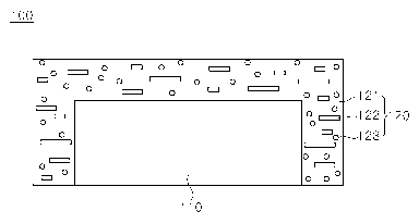
[6] Accordingly, the light transmissive resin undergoes significant
expansion or
Date Recue/Date Received 2021-06-30
CA 03125544 2021-06-30
2
contraction due to temperature variation of the light emitting diode chip or
for other
reasons. Since there is a significant difference in the degree of contraction
or
expansion due to temperature variation between the light emitting diode chip
and the
light transmissive resin, cracks are generated in the light transmissive
resin. When
the cracks are generated in the light transmissive resin, the light emitting
diode
package and a display device including the light emitting diode package suffer
from
deterioration in reliability.
[Disclosure]
[Technical Problem]
[7] Embodiments of the present disclosure provide a light emitting diode
package that has improved reliability by preventing generation of cracks.
[8] Embodiments of the present disclosure provide a light emitting diode
package that minimizes deterioration in luminous efficacy while improving
reliability.
[Technical Solution]
[9] In accordance with embodiments of the present disclosure, a light
emitting
diode package includes: a light emitting diode chip emitting light and a light
transmissive member. The light transmissive member covers at least an upper
surface of the light emitting diode chip and includes a light transmissive
resin and
reinforcing fillers. The reinforcing fillers have at least two side surfaces
having
different lengths and are dispersed in the light transmissive resin.
[Advantageous Effects]
[10] According to embodiments of the present disclosure, a light emitting
diode
package employs reinforcing fillers having a low coefficient of thermal
expansion to
Date Recue/Date Received 2021-06-30
CA 03125544 2021-06-30
3
prevent cracking in a light transmissive resin while improving reliability.
[11] According to embodiments of the present disclosure, the light emitting
diode package employs light transmissive reinforcing fillers to improve
reliability
while minimizing deterioration in luminous efficacy.
[Description of Drawings]
[12] FIG. 1 is a view of a light emitting diode package according to a
first
embodiment of the present disclosure.
[13] FIG. 2 and FIG. 3 are scanning electron microscope (SEM) images of a
conventional light emitting diode package.
[14] FIG. 4 is an SEM image of the light emitting diode package according
to
the first embodiment of the present disclosure.
[15] FIG. 5 is an SEM image of a light emitting diode package according to
a
second embodiment of the present disclosure.
[16] FIG. 6 is an SEM image of a light emitting diode package according to
a
third embodiment of the present disclosure.
[17] FIG. 7 is an SEM image of a light emitting diode package according to
a
fourth embodiment of the present disclosure.
[Best Mode]
[18] Hereinafter, embodiments of the present disclosure will be described
in
detail with reference to the accompanying drawings. The following embodiments
are
provided by way of example so as to fully convey the spirit of the present
disclosure
to those skilled in the art to which the present disclosure pertains.
Accordingly, the
present disclosure is not limited to the embodiments disclosed herein and can
also be
implemented in different forms. In the drawings, widths, lengths, thicknesses,
and
the like of elements can be exaggerated for clarity and descriptive purposes.
Throughout the specification, like reference numerals denote like elements
having
the same or similar functions.
Date Recue/Date Received 2021-06-30
CA 03125544 2021-06-30
4
[19] In accordance with embodiments of the present disclosure, a light
emitting
diode package includes: a light emitting diode chip emitting light and a light
transmissive member. The light transmissive member covers at least an upper
surface of the light emitting diode chip and includes a light transmissive
resin and
reinforcing fillers. The reinforcing fillers have at least two side surfaces
having
different lengths and are dispersed in the light transmissive resin.
[20] The reinforcing fillers may include at least one selected from the
group of
glass fibers formed of Si, Al, Fe, Ba, Ca, Mg and Na.
[21] Further, the reinforcing fillers may include at least one selected
from the
group of glass fibers formed of 5i02, A1203, MgO, CaO, Na2O, K20 and B203.
[22] The reinforcing fillers may be present in an amount of 10% by weight
(wt%)
to 200 wt% relative to the light transmissive resin.
[23] The reinforcing fillers may be present in an amount of 50 wt% to 100
wt%
relative to the light transmissive resin.
[24] According to one embodiment, the light transmissive member may cover
upper and side surfaces of the light emitting diode chip.
[25] The light emitting diode package may further include a barrier member
covering a side surface of the light transmissive member and reflecting light
emitted
through the side surface of the light emitting diode chip.
[26] The barrier member may further include the reinforcing fillers.
[27] According to another embodiment, the light transmissive member may
cover an upper surface of the light emitting diode chip.
[28] The light emitting diode package may further include a barrier member
covering a side surface of the light emitting diode chip.
[29] The barrier member may further include the reinforcing fillers.
[30] The light transmissive member may further cover an upper surface of
the
barrier member.
[31] The barrier member may further cover a side surface of the light
transmissive member.
[32] The light transmissive member may further include a wavelength
conversion material dispersed in the light transmissive resin.
Date Recue/Date Received 2021-06-30
CA 03125544 2021-06-30
[33] Hereinafter, light emitting diode packages according to embodiments of
the
present disclosure will be described in detail with reference to the
accompanying
drawings.
[34] FIG. 1 is a view of a light emitting diode package according to a
first
embodiment of the present disclosure.
[35] The light emitting diode package 100 according to the first embodiment
includes a light emitting diode chip 110 and a light transmissive member 120.
[36] The light emitting diode chip 110 includes a GaN-based semiconductor
stack grown on a growth substrate for growth of semiconductor layers. The
light
emitting diode chip 110 emits UV light or visible light.
[37] The light emitting diode chip 110 may include electrodes (not shown)
on at
least one of upper and lower portions thereof. For example, the electrodes may
be
formed at the upper portion of the light emitting diode chip 110 to be
electrically
connected to an external component by wire bonding. Alternatively, the
electrodes
may be formed at the lower portion of the light emitting diode chip 110 to be
electrically connected to an external component by flip chip bonding.
Alternatively,
the electrodes of the light emitting diode chip 110 may be formed at the upper
and
lower portions thereof, respectively, in which the electrode formed at the
lower
portion of the light emitting diode chip 110 is electrically connected to the
external
component by flip chip bonding and the electrode formed at the upper portion
thereof is electrically connected to the external component by wire bonding.
[38] The light transmissive member 120 covers a light emitting surface of
the
light emitting diode chip 110. For example, the light transmissive member 120
covers upper and side surfaces of the light emitting diode chip 110. With this
structure, the light transmissive member 120 can protect the light emitting
diode
chip 110 from an external environment.
[39] In addition, the transmissive member 120 may be formed a portion
covering the side surfaces of the light emitting diode chip 110 thicker than a
portion
covering the upper surface of the light emitting diode chip 110. That is, a
thickness
from the side surface of the light emitting diode chip 110 to the side surface
of the
transmissive member 120 is thicker than a thickness from the upper surface of
the
Date Recue/Date Received 2021-06-30
CA 03125544 2021-06-30
6
light emitting diode chip 110 to the upper surface of the transmissive member
120.
[40] The light transmissive member 120 includes a light transmissive resin
121,
reinforcing fillers 122, and a wavelength conversion material 123. The
reinforcing
fillers 122 and the wavelength conversion material 123 are formed of light
transmissive materials and dispersed in the light transmissive resin 121. If
non-
transmissive materials, such as typical metal fillers or carbon fillers, are
dispersed in
the light transmissive resin 121, luminous efficacy of the light emitting
diode
package can be deteriorated. Thus, the light emitting diode package 100
according to
this embodiment can prevent or minimize deterioration in luminous efficacy
using
the reinforcing fillers 122, which are light transmissive.
[41] For example, the light transmissive resin 121 may include at least one
selected from the group of a silicone resin, an epoxy resin, and a polyimide
resin.
However, it should be understood that these materials are provided by way of
example and the materials for the light transmissive resin 121 are not limited
thereto.
The light transmissive resin 121 may be a resin selected from any materials
that
allow transmission of light therethrough.
[42] The light transmissive resin 121 may have a higher coefficient of
thermal
expansion than the light emitting diode chip 110. Further, since the light
transmissive resin 121 contacts the light emitting diode chip 110, light and
heat
emitted from the light emitting diode chip 110 are directly transferred to the
light
transmissive resin 121.
[43] Accordingly, in a conventional light emitting diode package, the light
transmissive resin is degraded by light and heat emitted from the light
emitting diode
chip and suffers from cracking. Reliability of the light emitting diode
package is
deteriorated due to intrusion of foreign matter, such as moisture, air, dust,
and the
like, into the light emitting diode package through cracks or due to discharge
of light
not subjected to wavelength conversion through the cracks.
[44] The light emitting diode package 100 according to this embodiment
includes the reinforcing fillers 122 dispersed in the light transmissive resin
121. The
reinforcing fillers 122 prevent deterioration in reliability of the light
emitting diode
package due to difference in coefficient of thermal expansion between the
light
Date Recue/Date Received 2021-06-30
CA 03125544 2021-06-30
7
transmissive resin 121 and the light emitting diode chip 110.
[45] The reinforcing fillers 122 has at least two side surfaces having
different
lengths. For example, the reinforcing fillers 122 may have an elongated rod
structure
having a major axis and a minor axis.
[46] The reinforcing fillers 122 may include at least one selected from the
group
of glass fibers formed of Si, Al, Fe, Ba, Ca, Mg and Na. For example, the
reinforcing fillers 122 may include at least one selected from the group of
glass
fibers formed of SiO2, A1203, MgO, CaO, Na2O, K20 and B203.
[47] In the light transmissive member 120, the reinforcing fillers 122 may
be
present in an amount of 10 wt% to 200 wt% relative to the light transmissive
resin
121. Alternatively, in the light transmissive member 120, the reinforcing
fillers 122
may be present in an amount of 50 wt% to 100 wt% relative to the light
transmissive
resin 121.
[48] Glass fibers are resistant to heat and have a low coefficient of
thermal
expansion. In addition, the glass fibers are not affected by light and have
good
chemical resistance. Thus, the reinforcing fillers 122 formed of the glass
fibers also
have a low coefficient of thermal coefficient and exhibit good properties in
terms of
heat resistance and chemical resistance.
[49] Since the reinforcing fillers 122 have a low coefficient of thermal
expansion, it is possible to reduce the degree of expansion or contraction of
the light
transmissive resin 121 due to temperature variation. Accordingly, the
reinforcing
fillers 122 can prevent generation of cracks in the light transmissive resin
121.
Further, the reinforcing fillers 122 can prevent foreign matter from entering
the light
transmissive resin 121 through cracks by preventing cracking of the light
transmissive resin 121.
[50] Further, since the reinforcing fillers 122 have an elongated rod
structure,
the reinforcing fillers 122 block a progression route of the cracks to prevent
progression of the cracks. Furthermore, the reinforcing fillers 122 having an
elongated rod structure can obstruct foreign matter from entering the light
transmissive resin 121. Furthermore, even when foreign matter enters the light
transmissive resin 121, the elongated rod structure of the reinforcing fillers
122
Date Recue/Date Received 2021-06-30
CA 03125544 2021-06-30
8
extends an infiltration route of the foreign matter.
[51] As such, the light emitting diode package 100 according to this
embodiment includes the reinforcing fillers 122 to improve heat resistance and
chemical resistance of the light transmissive member 120, thereby improving
reliability.
[52] The wavelength conversion material 123 converts wavelengths of light
emitted from the light emitting diode chip 110 such that the light emitting
diode
package 100 can emit light having a predetermined color. For example, the
wavelength conversion material 123 may include at least one selected from
among
phosphors and quantum dots (QD).
[53] Although the light transmissive member 120 is illustrated as including
the
wavelength conversion material 123 in this embodiment, it should be understood
that the light transmissive member 120 is not required to include the
wavelength
conversion material 123. If light emitted from the light emitting diode
package 100
has the same wavelength band as light emitted from the light emitting diode
chip
110, the wavelength conversion material 123 can be omitted.
[54] When the light transmissive member 120 is not required to convert the
wavelengths of light emitted from the light emitting diode chip 110, the light
transmissive member 120 may not include the wavelength conversion material
123.
[55] Tables 1 and 2 show experimental results comparing reliability of
conventional light emitting diode packages 10, 20 with reliability of the
light
emitting diode package 100 according to this embodiment.
[56] A first experimental group and a second experimental group are
conventional light emitting diode packages 10, 20, respectively.
[57] FIG. 2 is an SEM image of the conventional light emitting diode
package
corresponding to the first experimental group and FIG. 3 is an SEM image of
the
conventional light emitting diode package 20 corresponding to the second
experimental group. The SEM images are pictures photographed by a scanning
electron microscope.
[58] Referring to FIG. 2, in the conventional light emitting diode package
10
corresponding to the first experimental group, a light transmissive member 11
Date Recue/Date Received 2021-06-30
CA 03125544 2021-06-30
9
includes a light transmissive resin 121 and a wavelength conversion material
123
dispersed in the light transmissive resin 121, and does not include fillers.
[59] Referring to FIG. 3, in the conventional light emitting diode package
20
corresponding to the second experimental group, a light transmissive member 21
includes a light transmissive resin 121, a wavelength conversion material 123,
and
fillers 22. In the second experimental group, the fillers 22 have a general
structure
instead of the elongated rod structure of the reinforcing fillers 122
according to this
embodiment and are present in an amount of 80 wt%. For example, the fillers 22
may be silica fillers.
[60] Third to seventh experimental groups are the light emitting diode
packages
100 according to this embodiment.
[61] FIG. 4 is an SEM image of the light emitting diode package according
to
this embodiment corresponding to the third to seventh experimental groups.
[62] In the light emitting diode package 100 according to this embodiment
corresponding to the third to seventh experimental groups, the light
transmissive
member 120 includes the light transmissive resin 121, the wavelength
conversion
material 123, and the reinforcing fillers 122. The reinforcing fillers 122
have an
elongated rod structure, as shown in FIG. 4.
[63] The reinforcing fillers 122 are present in an amount of 5 wt% in the
third
experimental group, in an amount of 10 wt% in the fourth experimental group,
in an
amount of 50 wt% in the fifth experimental group, in an amount of 100 wt% in
the
sixth experimental group, and in an amount of 150 wt% in the seventh
experimental
group.
[64] Table 1 shows experimental results comparing points of times at which
cracks are generated in the light transmissive members 11, 21, 120 of the
conventional light emitting diode packages 10, 20 and the light emitting diode
package 100 according to this embodiment.
[65] The experiment was performed while supplying an electric current of
1,000
mA to the light emitting diode chip 110 at 100 C in each of the experimental
groups.
[66] Table 1
Kind Experimental time (hour)
Date Recue/Date Received 2021-06-30
CA 03125544 2021-06-30
500 1000 1500 2000 2500 3000 3500
First experimental group Pass Crack - - - -
Second experimental group Pass Crack - - - - -
Third experimental group Pass Crack - - - -
Fourth experimental group Pass Pass Crack - - - -
Fifth experimental group Pass Pass Pass Pass Crack - -
Sixth experimental group Pass Pass Pass Pass Pass Pass
Crack
Seventh experimental group Pass Pass Pass Pass Pass Pass
Crack
[67] Referring to Table 1, in all of the first experimental group, the
second
experimental group and the third experimental group, cracks were generated in
the
light transmissive members 11, 21, 120 when the experiment was performed for
1,000 hours. From this result, it can be seen that the general fillers 22 not
having an
elongated rod shape failed to prevent cracking of the light transmissive
member 21
and to improve reliability of the light emitting diode package 20. Further, it
can be
seen that the light emitting diode package containing 5 wt% or less of the
reinforcing fillers 122 did not exhibit a significant difference in
reliability with the
conventional light emitting diode packages.
[68] However, in all of the fourth to seventh experimental groups, cracks
were
generated when the experiment was performed for 1,500 hours or more.
Accordingly,
it can be seen that the light emitting diode package 100 including the light
transmissive member 120 containing 10 wt% or more of the reinforcing fillers
122
had better reliability than the conventional light emitting diode packages 10,
20.
[69] Further, in the fifth experimental group, cracks were generated when
the
experiment was performed for 2,500 hours, indicating a significant difference
from
the fourth experimental group in which cracks were generated when the
experiment
was performed for 1,500 hours. Further, in the sixth and seventh experimental
groups, cracks were generated when the experiment was performed for 3,500
hours,
indicating a significant difference from the fifth experimental group in which
cracks
were generated when the experiment was performed for 2,500 hours.
[70] It should be noted that, when the content of the reinforcing fillers
122
exceeds 200 wt%, it is difficult to apply the reinforcing fillers 122 to
experiments
and packages due to increase in viscosity of the light transmissive member,
which
makes it difficult to form the light transmissive member.
[71] From these experiments, it can be seen that reliability of the light
emitting
Date Recue/Date Received 2021-06-30
CA 03125544 2021-06-30
11
diode package 100 is improved when the reinforcing fillers 122 are present in
an
amount of 10 wt% to 200 wt% in the light transmissive member 120. In addition,
it
can be seen that reliability of the light emitting diode package 100 is
improved to a
significant level when the reinforcing fillers 122 are present in an amount of
50 wt%
or more in the light transmissive member 120. Further, it can be seen that
reliability
of the light emitting diode package 100 is improved to a significant level
when the
reinforcing fillers 122 are present in an amount of 100 wt% or more in the
light
transmissive member 120.
[72] That is, the light emitting diode package 100 according to this
embodiment
has improved reliability when the light transmissive member 120 includes 10
wt% to
200 wt% of the reinforcing fillers 122.
[73] Furthermore, the light emitting diode package 100 has further improved
reliability when the light transmissive member 120 includes 50 wt% to 200 wt%
or
100 wt% to 200 wt% of the reinforcing fillers 122.
[74] Table 2 shows luminous flux depending upon the content of the
reinforcing
fillers 122 in the light emitting diode package 100 according to this
embodiment
upon application of an electric current of 350 mA to the light emitting diode
chip
110.
[75] Table 2
Kind Luminous Flux (1m) Remark
First experimental group 102.82 100%
Third experimental group 102.61 99.8%
Fourth experimental group 101.90 99.3%
Fifth experimental group 100.57 98.7%
Sixth experimental group 98.56 98.0%
Seventh experimental group 95.41 96.8%
[76] Referring to Table 2, with reference to the luminous flux of the first
experimental group not including the fillers, the luminous flux of the third
to seventh
experimental groups each including the reinforcing fillers 122 was decreased.
The
third experimental group has a difference in luminous flux of 0.2% with the
first
experimental group. The fourth experimental group has a difference in luminous
flux of 0.7% with the first experimental group and a difference in luminous
flux of
0.5% with the third experimental group. The fifth experimental group has a
difference in luminous flux of 1.3% with the first experimental group and a
Date Recue/Date Received 2021-06-30
CA 03125544 2021-06-30
12
difference in luminous flux of 0.6% with the fourth experimental group. The
sixth
experimental group has a difference in luminous flux of 2% with the first
experimental group and a difference in luminous flux of 0.7% with the fifth
experimental group. The seventh experimental group has a difference in
luminous
flux of 3.2% with the first experimental group and a difference in luminous
flux of
1.2% with the sixth experimental group. The third to sixth experimental groups
having a difference in luminous flux of 2% or less with the first experimental
group
have a luminous flux reduction rate of 0.7% or less as the content of the
reinforcing
fillers 122 increases. However, the seventh experimental group has a
difference in
luminous flux of 1.2% with the sixth experimental group and exhibits rapid
increase
in luminous flux reduction rate.
[77] From this experiment, it can be seen that the reinforcing fillers 122
are
present in an amount of 100 wt% of less in the light transmissive member 120
in
order to minimize deterioration in luminous efficacy of the light emitting
diode
package 100.
[78] That is, the light emitting diode package 100 according to this
embodiment
has improved reliability when the light transmissive member 120 includes 10
wt% to
200 wt% of the reinforcing fillers 122.
[79] Furthermore, the light emitting diode package 100 according to this
embodiment has further improved reliability when the light transmissive member
120 includes 50 wt% to 200 wt% of the reinforcing fillers 122 than when the
light
transmissive member 120 includes less than 50 wt% of the reinforcing fillers
122.
[80] Furthermore, the light emitting diode package 100 according to this
embodiment has significantly improved reliability while minimizing
deterioration in
luminous efficacy when the light transmissive member 120 includes 50 wt% to
100
wt% of the reinforcing fillers 122.
[81] The light emitting diode package 100 may be manufactured by a method
including: preparing a support substrate (not shown); placing light emitting
diode
chips 110 on the support substrate; forming a light transmissive member 120;
polishing an upper surface of the light transmissive member 120; performing a
singulation process; and removing the support substrate.
Date Recue/Date Received 2021-06-30
CA 03125544 2021-06-30
13
[82] First, multiple light emitting diode chips 110 may be placed on the
support
substrate. Here, the multiple light emitting diode chips 110 may be placed to
be
separated from each other.
[83] Then, the light transmissive member 120 may be formed on the support
substrate to cover the multiple light emitting diode chips 110.
[84] Next, the upper surface of the light transmissive member 120 may be
polished. During polishing of the upper surface of the light transmissive
member
120, the reinforcing fillers 122 may be exposed through the upper surface of
the
light transmissive member 120.
[85] Next, the singulation process is performed by dicing the light
transmissive
member 120 between the light emitting diode chips 110 to provide individual
light
emitting diode packages 100. Here, during dicing of the light transmissive
member
120, the reinforcing fillers 122 may be exposed through the side surface of
the light
transmissive member 120.
[86] Next, the support substrate is removed, thereby providing the
individual
light emitting diode packages 100, as shown in FIG. 1.
[87] In the following description of light emitting diode packages
according to
other embodiments, the same components as those of the light emitting diode
package according to the above embodiment will be omitted or briefly
described.
For details of the omitted or briefly described components, refer to the
descriptions
of the above embodiment.
[88] FIG. 5 is an SEM image of a light emitting diode package according to
a
second embodiment of the present disclosure.
[89] The light emitting diode package 200 according to the second
embodiment
includes a light emitting diode chip 110, a light transmissive member 120, and
a
barrier member 210.
[90] The light transmissive member 120 covers upper and side surfaces of
the
light emitting diode chip 110. In addition, the light transmissive member 120
includes a light transmissive resin 121, reinforcing fillers 122, and a
wavelength
conversion material 123. The reinforcing fillers 122 and the wavelength
conversion
material 123 are dispersed in the light transmissive resin 121. Here, the
wavelength
Date Recue/Date Received 2021-06-30
CA 03125544 2021-06-30
14
conversion material 123 may be omitted depending upon wavelengths of light
emitted from the light emitting diode chip 110.
[91] The barrier member 210 is formed of a material capable of reflecting
light
and reflects light emitted from the light emitting diode chip 110. For
example, the
barrier member 210 may include at least one selected from the group of a
silicone
resin, an epoxy resin, and a mixture thereof. Further, the barrier member 210
may
include a reflective material, such as TiO2, SiO2, and A1203, in order to
improve
light transmittance.
[92] According to this embodiment, the barrier member 210 covers a side
surface of the light transmissive member 120 and exposes an upper surface of
the
light transmissive member 120. That is, the barrier member 210 reflects light
emitted through the side surface of the light emitting diode chip 110 such
that the
light can be emitted through the upper surface of the light transmissive
member 120.
Accordingly, the barrier member 210 may improve luminous efficacy of the light
emitting diode package 200 by preventing light loss through the side surface
of the
light emitting diode package 200.
[93] Further, the barrier member 210 prevents foreign matter from entering
the
light transmissive member 120 and the light emitting diode chip 110 through
the
side surface of the light emitting diode package 200, thereby improving
reliability of
the light emitting diode package 200.
[94] The barrier member 210 may include the reinforcing fillers 122.
[95] The reinforcing fillers 122 have a low coefficient of thermal
expansion to
suppress expansion or contraction of the barrier member 210 due to temperature
variation. Accordingly, the barrier member 210 can secure the light
transmissive
member 120 such that the light transmissive member 120 does not suffer from
variation in length or volume due to temperature variation. Further, the
barrier
member 210 can prevent the light transmissive member 120 from being peeled off
of
the light emitting diode chip 110.
[96] In addition, the reinforcing fillers 122 having an elongated rod
structure can
prevent foreign matter from entering the light emitting diode package 200
through
the barrier member 210. Further, even when foreign matter enters the barrier
Date Recue/Date Received 2021-06-30
CA 03125544 2021-06-30
member 210, the reinforcing fillers 122 having an elongated rod structure can
prevent the foreign matter from reaching the light transmissive member 120 by
blocking or extending an intrusion route of the foreign matter.
[97] Accordingly, the barrier member 210 including the reinforcing fillers
122
can prevent components of the light emitting diode package 200 from being
degraded due to effects of foreign matter.
[98] Although the barrier member 210 is illustrated as including the
reinforcing
fillers 122, it should be understood that the reinforcing fillers 122 can be
omitted so
long as it is possible to prevent deterioration in reliability of the light
emitting diode
package 200 while sufficiently preventing foreign matter from entering the
light
emitting diode package 200 even without the reinforcing fillers 122.
[99] FIG. 6 is an SEM image of a light emitting diode package according to
a
third embodiment of the present disclosure.
[100] FIG. 7 is an SEM image of a light emitting diode package according to a
fourth embodiment of the present disclosure.
[101] Each of the light emitting diode packages 300, 400 according to the
third
and fourth embodiments includes a light emitting diode chip 110, a light
transmissive member 120, and a barrier member 210.
[102] The light transmissive member 120 covers an upper surface of the light
emitting diode chip 110. In addition, the light transmissive member 120
includes a
light transmissive resin 121, reinforcing fillers 122, and a wavelength
conversion
material 123. The reinforcing fillers 122 and the wavelength conversion
material
123 are dispersed in the light transmissive resin 121. Here, the wavelength
conversion material 123 may be omitted depending upon wavelengths of light
emitted from the light emitting diode chip 110.
[103] Referring to FIG. 6, in the light emitting diode package 300 according
to
the third embodiment, the barrier member 210 covers a side surface of the
light
emitting diode chip 110 and a side surface of the light transmissive member
120.
[104] Referring to FIG. 7, in the light emitting diode package 400 according
to
the fourth embodiment, the barrier member 210 is disposed at a lower side of
the
light transmissive member 120 and covers a side surface of the light emitting
diode
Date Recue/Date Received 2021-06-30
CA 03125544 2021-06-30
16
chip 110. That is, in the light emitting diode package 400 according to the
fourth
embodiment, the light transmissive member 120 covers an upper surface of the
light
emitting diode chip 110 and an upper surface of the barrier member 210.
[105] The barrier member 210 is formed of a material capable of reflecting
light
and reflects light emitted from the light emitting diode chip 110. For
example, the
barrier member 210 may include at least one selected from the group of a
silicone
resin, an epoxy resin, and a mixture thereof. Further, the barrier member 210
may
include a reflective material, such as TiO2, SiO2, and A1203, in order to
improve
light transmittance.
[106] The barrier member 210 may include the reinforcing fillers 122 dispersed
therein. The barrier member 210 including the reinforcing fillers 122 can
secure the
light transmissive member 120 such that the light transmissive member 120 does
not
suffer from variation in length or volume due to temperature variation. In
addition,
the reinforcing fillers 122 of the barrier member 210 can prevent foreign
matter from
entering the light emitting diode packages 300, 400 through the barrier member
210.
[107] According to the third and fourth embodiments, the barrier member 210
covers the side surface of the light emitting diode chip 110 to reflect light
emitted
through the side surface of the light emitting diode chip 110. Light emitted
through
the side surface of the light emitting diode chip 110 is reflected by the
barrier
member 210 to travel towards the light transmissive member 120 disposed at an
upper side of the light emitting diode chip 110.
[108] Therefore, in the light emitting diode packages 300, 400 according to
the
third and fourth embodiments, the barrier member 210 can prevent light loss
through
the side surface of each of the light emitting diode packages 300, 400,
thereby
improving luminous efficacy.
[109] Although some embodiments have been described herein with reference to
the accompanying drawings, it should be understood that these embodiments are
provided for illustration only and are not to be construed in any way as
limiting the
present disclosure. Therefore, it should be understood that the scope of the
present
disclosure should be defined by the appended claims and equivalents thereto.
[110] <Reference Numerals>
Date Recue/Date Received 2021-06-30
CA 03125544 2021-06-30
17
10, 20, 100, 200, 300, 400: Light emitting diode package
22: Fillers
110: Light emitting diode chip
11, 21, 120: Light transmissive member
121: Light transmissive resin
122: Reinforcing fillers
123: Wavelength conversion material
210: Barrier member
Date Recue/Date Received 2021-06-30