Note : Les descriptions sont présentées dans la langue officielle dans laquelle elles ont été soumises.
CA 03133605 2021-09-14
P15-0010-CA
ARRANGEMENT OF A WAVEGUIDE ASSEMBLY AND ITS MANUFACTURING PROCESS
Technical field
[0001] The present invention relates to an arrangement for
telecommunication
satellites, comprising an assembly of waveguides for radio frequency signals.
The present
invention also relates to a method of designing and manufacturing this
arrangement.
State of the art
[0002] Waveguides are widely used in telecommunication satellites,
notably to
interconnect electronic components and equipment.
[0003] Conventional systems contain a large number of electronic
components and
equipment and therefore require a large number of waveguides, which are
typically
interconnected by assembling standard length elements, such as straight or
curved tubes,
with flanges screwed together to connect these electronic components and
equipment.
[0004] The use of waveguides made with standardized tubes imposes sub-
optimal paths
and complex interconnection layouts. This implies the use of long waveguides
which have the
disadvantages of degrading or attenuating signals transmitted in these guides
and increasing
the weight and footprint of the system.
[0005] Furthermore, the fixation of waveguides in the payload bay of a
communication
satellite requires stands or fixation systems screwed on the waveguides, which
implies
additional weight and complicates the assembly of conventional systems.
[0006] In order to ensure the necessary rigidity and stability of the
waveguides to
withstand the important mechanical constraints, in particular during the take-
off of the rocket
carrying the telecommunications satellite, it is known to oversize the
waveguides so that they
have a significant thickness and to fix them in the payload bay thanks to
numerous fixing
stands.
1
Date Recue/Date Received 2021-09-14
CA 03133605 2021-09-14
P15-0010-CA
[0007] Furthermore, in order to ensure that the waveguides and the
electronic
components and equipment operate in an optimal temperature range, it is
necessary to
integrate fins, radiators, dissipation elements, heat dissipation pipes, etc.
into the
conventional systems, which makes the assembly even more complex.
[0008] This can make the design of the system particularly complex to
ensure that all
waveguides and electronic components and equipment required by the system can
be
arranged within a predetermined footprint.
[0009] Conventional manufacturing processes impose constraints on the
freedom of the
designer of the system because complex waveguides have tight mechanical
tolerances in
.. order to achieve the desired RF performance. Therefore, care must be taken
to ensure that
waveguides can be constructed to achieve this performance.
[0010] Conventionally, waveguides are designed, manufactured and supplied
individually, and are manually assembled into a waveguide assembly using
fixation tools. This
approach allows optimizing the design of each waveguide based on its
performance and the
transmission characteristics presented to the RF signals passing through that
waveguide.
However, this implies significant assembly costs and completion times.
[0011] As system requirements evolve, requiring an increasingly complex
design, due to
the need for increased signal bandwidth and improved performance, the spatial
and weight
constraints for accommodating waveguides become increasingly important.
[0012] Conventional means of reducing the size and manufacturing time
associated with
waveguides include simplifying waveguide assembly, by reducing the size,
length, and/or
diameter of the waveguides. It is also possible to design more complex signal
processing
layouts so that information can be multiplexed onto a smaller number of
signals, requiring
fewer waveguides, for example, but at the expense of increasing the processing
load of a
demultiplexer.
[0013] W02018029455 discloses a waveguide assembly constructed such that
two or
more, and in some cases all, of the waveguides in the assembly are integrally
formed with
2
Date Recue/Date Received 2021-09-14
CA 03133605 2021-09-14
P15-0010-CA
one another. In the case of using waveguide connectors to enable interfacing
with other
waveguide assemblies, the waveguides of the assembly and one or more interface
flanges of
one or more respective waveguide connectors may be integrally formed. Such
integral
formation may be achieved using an additive manufacturing (AM) technique.
[0014] EP3439099 discloses a spacecraft comprising a power network that
includes a
plurality of unit modules. Each module includes a plurality of radio frequency
(RF) waveguides
structurally coupled together with at least one connecting element. For each
unit module, the
connection element and a wall structure defining the plurality of waveguides
are co-
fabricated using an additive manufacturing process. The power supply array may
also include
a cooling system such as a radiator
[0015] The power supply array according to EP3439099 is not, however,
suitable for
heating elements that might be arranged in locations in or outside the
spacecraft's payload
bay to ensure optimal operation of such elements.
[0016] The present invention therefore aims at providing an arrangement
of a waveguide
assembly, for telecommunication satellites, optimized according to the
complexity of the
arrangement, the spatial and weight constraints and which addresses the
drawbacks of the
prior art.
[0017] Another aim of the present invention is to provide an arrangement
of a waveguide
assembly optimized as a function of the number and type of electronic
equipment and/or
components to be integrated according to the constraints of a predetermined
specification
of a designer.
[0018] Another aim of the present invention is to provide an arrangement
of a waveguide
assembly that is easy to design and fast to manufacture.
[0019] Another aim of the present invention is to provide an arrangement
of a waveguide
assembly to which electronic components and/or equipment can be easily
connected.
3
Date Recue/Date Received 2021-09-14
CA 03133605 2021-09-14
P15-0010-CA
Brief summary of the invention
[0020] These aims are achieved by a satellite arrangement comprising a
payload bay. The
arrangement includes an assembly of waveguides, waveguide fixation interfaces
for fixing the
waveguides to electronic equipment and/or components, and a mechanical
structure
including a plurality of links interconnecting at least some of the waveguides
to provide
stability to the waveguide assembly. The arrangement further comprises at
least one heat
pipe that is arranged to heat or cool one or more of the waveguides. The
arrangement is
formed in one piece by 3D printing.
[0021] According to an embodiment, the mechanical structure connects the
heat pipe to
at least one waveguide.
[0022] According to an embodiment, the one-piece arrangement further
comprises at
least one antenna.
[0023] According to an embodiment, the antenna comprises an array of
multiple RF feed
chains incorporating a heat exchanger. The antenna is monolithic and further
comprises a
housing containing at least a portion of the array and comprising at least one
inlet and one
outlet in fluid communication with the heat exchanger.
[0024] According to an embodiment, the mechanical structure comprises a
multitude of
rigid links interconnecting the lateral surfaces of at least two waveguides at
different points.
[0025] According to an embodiment, the arrangement further comprises
fixation
elements for fixing the arrangement to the payload bay or to a support
connected to the
payload bay.
[0026] According to an embodiment, the arrangement further comprises one
or more
filters.
4
Date Recue/Date Received 2021-09-14
CA 03133605 2021-09-14
P15-0010-CA
[0027] Another aspect of the invention relates to a satellite assembly,
comprising the
arrangement described above and electronic equipment and/or components
connected to
the waveguide fixation interfaces.
[0028] According to an embodiment, one or more electronic equipment
and/or
components are selected from the group consisting of the following: switch,
circulator,
isolator, low noise amplifier, power amplifier, computer signal processing
unit, RF load, filter,
multiplexer, MMIC circuit and RF circuit.
[0029] According to an embodiment, the assembly further comprises
photovoltaic cell
panels that are connected to the mechanical structure.
[0030] Another aspect of the invention relates to a satellite arrangement
comprising a
payload bay. The arrangement comprises a waveguide assembly, waveguide
fixation
interfaces for fixing the waveguides to electronic equipment and/or
components, and a
mechanical structure comprising a plurality of links interconnecting at least
some of the
waveguides to provide stability to the waveguide assembly. The arrangement
further
comprises at least one antenna. The arrangement is formed in one piece by 3D
printing.
[0031] According to an embodiment, the antenna comprises an array of
multiple RF feed
chains incorporating a heat exchanger. The antenna further comprises a housing
containing
said array and comprising at least one input and one output in fluid
communication with the
heat exchanger.
[0032] Another aspect of the invention relates to a method of designing and
manufacturing the waveguide assembly arrangement as described above. In
particular, the
method includes the following steps:
- defining a footprint volume of the arrangement according to a predetermined
footprint volume;
- modelling the arrangement by computer by defining
the shape and length of each waveguide in the waveguide assembly
the shape of the mechanical structure, and
5
Date Recue/Date Received 2021-09-14
CA 03133605 2021-09-14
P15-0010-CA
the shape of the fixation interfaces required to connect the waveguide
assembly of
the arrangement to electronic equipment and/or components within the
constraints of the
predetermined footprint, and
- manufacturing the arrangement in a single piece according to the model shape
designed by computer with an additive manufacturing step.
[0033] According to an embodiment, the shape and length of each waveguide
required
for connection of the assembly of waveguides of the arrangement are further
determined
based on the number and type of electronic equipment and/or components to be
integrated
according to the constraints of a predetermined specification of a designer.
[0034] According to an embodiment, the shape and length of each waveguide
required
for the connection of the assembly of waveguides of the arrangement are
further determined
to optimize the performance of the satellite payload, and while respecting the
mechanical
and thermal constraints of the arrangement.
[0035] According to an embodiment, the shape of the mechanical structure
as well as
the shape of the heat transfer elements are determined, respecting the
constraints of the
predetermined footprint volume while optimizing the performance of the
satellite payload,
and respecting the mechanical and thermal constraints of the arrangement.
[0036] According to an embodiment, the method further comprises a step of
connecting
electronic equipment and/or components to the waveguide fixation interfaces.
[0037] According to an embodiment, the method further comprises a step of
connecting
photovoltaic cell panels to the mechanical structure of the arrangement.
Brief description of the figures
[0038] Examples of embodiments of the invention are indicated in the
description
illustrated by the appended figures in which:
6
Date Recue/Date Received 2021-09-14
CA 03133605 2021-09-14
P15-0010-CA
- Figure 1 represents a schematic view of an arrangement for
telecommunication
satellites, comprising notably an assembly of waveguides according to an
embodiment of
the invention;
- Figure 2 represents a schematic view of an arrangement for
telecommunication
satellites, comprising an assembly of waveguides connected to electronic
equipment and/or
components according to another embodiment;
- Figure 3 shows a schematic view of an arrangement for telecommunication
satellites arranged in the satellite payload bay, according to another
embodiment;
- Figures 4a, 4b, 4c illustrate different perspective views of an
arrangement for
telecommunication satellites comprising several waveguides and a heat pipe,
according to
another embodiment;
- Figure 5a illustrates a perspective view of a monolithic antenna
according to an
embodiment;
- Figure 5b illustrates a top view of Figure 5a;
- Figure Sc illustrates a cross-sectional view of Figure 5b along A-A;
- Figure 5d illustrates a perspective view of the antenna of Figure 5a
without its
housing, and
- Figure 6 illustrates a block diagram of a design and manufacturing
process
according to the different embodiments of the present invention.
Examples of embodiments of the invention
[0039] In the present invention, the term "arrangement" can be
interpreted as a
complete structure that can be fixed in the payload bay of the communications
satellite or a
7
Date Recue/Date Received 2021-09-14
CA 03133605 2021-09-14
P15-0010-CA
subassembly of the structure. In this case, the complete structure is obtained
by assembling
several subassemblies of the arrangement.
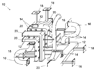
[0040] According to a first embodiment illustrated in Figure 1, the
arrangement 10, for
telecommunication satellites, comprises an assembly of waveguides 12
interconnected to
each other by a mechanical structure in order to ensure a satisfactory
rigidity/stability of the
assembly of waveguides 12 according to a predetermined configuration.
[0041] This predetermined configuration is dictated not only as a
function of a restricted
footprint volume available in the payload bay of the telecommunications
satellite, but also as
a function of the number and type of electronic equipment and components to be
integrated
into the payload bay according to the constraints of a predetermined
specification of a
designer.
[0042] The mechanical structure may include a plurality of rigid links 14
interconnecting
multiple waveguides 12 at different points along the length of the waveguides.
These rigid
links are, for example, in the form of rods made by 3D printing and arranged
so as to connect
two lateral surfaces together of at least two waveguides so that the
arrangement 10 can
withstand significant stresses, in particular during the takeoff of the rocket
carrying the
telecommunications satellite, while fulfilling the function of a damper
against the vibrations
generated, for example, during the rocket takeoff. The rods comprise each a
core, for example
made of polymer, and a metal jacket that provides rigidity.
[0043] The arrangement 10 may further comprise one or more heat dissipation
elements, for example in the form of one or more cooling fins 16a and/or one
or more heat
transport tubes 16b, for example in the form of a heat pipe for transporting
heat by means of
the principle of heat transfer by phase transition of a fluid. The arrangement
10 may also
include fixation elements, for example fixation stands 18, for fixing the
arrangement 10 to the
payload bay or to a support related to the payload bay of the communication
satellite.
[0044] Each waveguide 12 according to Figure 1 has a fixation interface
20 at both ends,
preferably in the form of a fixation flange. According to the configuration of
the arrangement
8
Date Recue/Date Received 2021-09-14
CA 03133605 2021-09-14
P15-0010-CA
10, the waveguides 12 are arranged so that they can be connected, via their
respective
fixation flanges, to different electronic equipment and/or components.
[0045] Advantageously, the arrangement 10 is formed in a single piece
made by additive
manufacturing methods, for example 3D printing. In particular, additive
manufacturing of
waveguides comprising both non-conductive materials, such as polymers or
ceramics, and
conductive metals is known. Waveguides comprising ceramic or polymer walls
manufactured
by an additive method and then covered with a metal plating have notably been
suggested.
The use of a non-conductive core allows, on the one hand, to reduce the weight
and cost of
the arrangement 10 and, on the other hand, to implement 3D printing methods
adapted to
polymers or ceramics and allowing to produce high precision parts with low
roughness.
[0046] WO 2017208153, the contents of which are incorporated by
reference, discloses
in particular a waveguide device for guiding a radio frequency signal at a
specified frequency.
The device includes a core fabricated by additive manufacturing and including
sidewalls with
inner surfaces defining a waveguide channel and a metallic conductive layer
covering the
inner surface of the core.
[0047] Additive manufacturing makes it possible to produce different
configurations of
the arrangement of waveguides 12, whose trajectory of each guide 12 is
previously calculated
and modeled by computer in order to optimize the footprint of the arrangement
10 by taking
into account a particular specification of a designer. This process allows not
only to obtain an
optimal configuration of the arrangement 10 but also and especially a fast and
easy
manufacturing with a simplified assembly compared to conventional systems.
Moreover, the
realization of the arrangement in a single piece by an additive manufacturing
step allows to
print shapes impossible to assemble by conventional assembly processes.
[0048] According to another embodiment illustrated in Figure 2, the
arrangement 110 is
not intended to be mounted on a panel or stand. This arrangement 110 is
connected only to
electronic equipment and components 122 including one or more amplifiers, and
to a
computer processing unit to obtain an assembly 50 that can be connected to the
payload bay
(not shown), directly or indirectly.
9
Date Recue/Date Received 2021-09-14
CA 03133605 2021-09-14
P15-0010-CA
[0049] Like the arrangement 10 according to the first embodiment, the
arrangement 110
of Figure 2 comprises an assembly of waveguides 112 interconnected to one
another by a
multitude of links in the form of rigid rods 114 interconnecting the
waveguides 112 at
different points along their respective lengths in order, on the one hand, to
ensure
satisfactory rigidity of the arrangement 110 and, on the other hand, to ensure
that this
arrangement 110 can withstand significant stress.
[0050] The arrangement 110 may further include one or more heat
dissipation elements
which may also be in the form of one or more cooling fins 116a and/or one or
more heat
transport tubes 116b (e.g., heat pipe). As in the first embodiment, each
waveguide 112
includes an fixation interface 120 at both ends, preferably in the form of an
fixation flange
also integrally formed with the waveguide. The fixation flanges at the
respective ends of the
waveguides 112 may, for example, be connected respectively to two pieces of
electronic
equipment to transfer radio frequency signals from one piece of electronic
equipment to the
other.
[0051] Like the arrangement 10 according to the first embodiment, the
arrangement 110
of Figure 2 is made of a single piece obtained by an additive manufacturing
process having
the advantages mentioned above. The assembly 50 of Figure 2 is obtained by an
additional
manufacturing step of connecting electronic equipment and/or components 122 to
the
fixation interfaces 120 of the waveguides 112.
[0052] According to another embodiment illustrated in Figure 3, the
arrangement 210
comprises an assembly of waveguides 212, a mechanical structure 214, one or
more heat
dissipation elements, e.g., one or more cooling fins 216a and/or one or more
cooling tubes
216b, one or more filters 240 and at least one antenna 230. The filters 240
are, for example,
connected to an amplifier 222 which is arranged to communicate with a computer
processing
unit 224. The amplifier 222 and the computer processing unit 224 are in
contact with at least
one heat dissipating element to dissipate heat generated by the amplifier and
the computer
unit. According to this configuration, a portion of the arrangement 210 may be
disposed
outside the payload bay 300.
Date Recue/Date Received 2021-09-14
CA 03133605 2021-09-14
P15-0010-CA
[0053] Waveguides 212 connect the filters to the antenna 230. The
mechanical structure
214 is configured to support the electronic equipment and components 222, 224,
the antenna
230, and a plurality of photovoltaic cell panels 250.
[0054] Like the arrangement 10, 110 according to the first two
embodiments, the
arrangement 210 of Figure 3 is in the form of a single piece made by an
additive
manufacturing process having the advantages discussed above. The assembly 50
of Figure 3
is obtained by an additional manufacturing step of connecting electronic
equipment and/or
components 222, 224 to the assembly of waveguides 212, via the waveguide
fixation flanges
220, and the photovoltaic cell panels 250 to the arrangement 210, in
particular to the
mechanical structure 214 of the arrangement.
[0055] According to another embodiment illustrated in Figures 4a to 4c,
the arrangement
310 includes an assembly of waveguides 312 interconnected together by a
mechanical
structure 314 to rigidify the assembly of waveguides, and including fixation
interfaces 320 to
attach the waveguides 312 to, for example, RF components. This arrangement has
the
particularity of further comprising a heat pipe 316 in the form of a hermetic
enclosure that
contains a fluid in a liquid-vapor equilibrium state. The heat pipe 316 has
grooves or fins along
its inner surface to ensure the return of the fluid by capillary action. All
of the aforementioned
elements of the arrangement 310 is in one piece made by 3D printing.
[0056] The advantage of the heat pipe 316 is that it not only allows for
the cooling of
certain elements, for example the cooling of one or more waveguides 312 when
they are
located in a location in the payload bay of a communication satellite where a
high
temperature prevails, but also allows for the heating of one or more
waveguides 312 or other
elements when they are situated in a location inside the payload bay where a
lower
temperature prevails, or when these waveguides or other elements are situated
outside the
payload bay. Thus, the use of a heat pipe provides adequate temperature
control of the
waveguides or other elements for their optimal operation.
[0057] According to an embodiment, the arrangement formed in one piece by
3D
printing comprises one or more monolithic antennas. The antenna may, for
example, be of
11
Date Recue/Date Received 2021-09-14
CA 03133605 2021-09-14
P15-0010-CA
the type illustrated in Figures 5a to 5d. The antenna 500 includes a housing
502 containing an
array 550 of a plurality of RF feed chains 510, for example 19 RF feed chains.
Each chain 510
includes a horn 510a, a polarizer 510b and a filter 510.
[0058] The array 550 integrates a heat exchanger 560 which can have
different structures
to promote calorific exchanges, notably of the lattice, honeycomb or cellular
type. To this end,
the housing 502 includes one or more inlets 520a and one or more outlets 520b
in fluid
communication with the heat exchanger.
[0059] The design and manufacturing process according to Figure 6 can be
adapted to
any type of arrangement according to the invention. The arrangement may
comprise, for
example, a limited number of waveguides or, on the contrary, for complex
systems, a large
number of waveguides. For these complex systems, the modelling of the optimal
waveguide
trajectories is calculated by computer according to different parameters, in
particular
according to the number and type of equipment and/or electronic components
that the
waveguides must connect and the volume of space available for its installation
in the payload
bay of a telecommunications satellite. The optimal trajectories of the
waveguides must also
be modeled to optimize the performance of the satellite payload, while
respecting the
mechanical and thermal constraints of the arrangement.
12
Date Recue/Date Received 2021-09-14