Note : Les descriptions sont présentées dans la langue officielle dans laquelle elles ont été soumises.
CA 03134609 2021-09-22
WO 2020/198480 PCT/US2020/024971
ARTICLE HAVING A HIGH VISIBLE LIGHT REFLECTANCE AND A NEUTRAL COLOR
CROSS REFERENCE TO RELATED APPLICATIONS
[0001] The present application is entitled to and claims priority to United
States Provisional
Application No. 62/976,645 filed February 14, 2020 and United States
Provisional Application No.
62/825,326 filed March 28, 2019, the disclosures of which are incorporated by
reference.
BACKGROUND OF THE INVENTION
Field of the Invention
[0002] The invention relates generally to vehicle transparencies, such as
vehicle windshields,
and in one particular embodiment, a windshield having a high visible light
reflectance and neutral
color.
Technical Considerations
[0003] In the automotive market, there is a heavy emphasis is placed on
vehicle styling. The
way a vehicle looks can be as important to vehicle sales as the vehicle's
mechanical reliability or
safety rating. Therefore, automotive manufacturers have gone to great lengths
to enhance
vehicle styling. These styling enhancements include providing more color
selections to the
consumer and also providing colors having metallic flakes to provide a vehicle
with a
"photochromic effect".
[0004] While these styling enhancements have been generally well received by
consumers, a
problem to date is that even with the new vehicle paint finishes, the
automotive transparencies
(such as but not limited to windshields, side lights, back lights, moon roofs,
and sun roofs)
continue to be generally gray or neutral colored. While providing solar
control properties, these
conventional transparencies provide little enhancement to the vehicle styling.
[0005] In the non-automotive fields, it has been known to provide coated
articles in which a
color is generated by the interference effect between a substrate and a
coating. As will be
appreciated by one skilled in the art, the term "interference effect" refers
to the variation of
electromagnetic wave amplitude with distance or time, caused by the
superposition of waves of
electromagnetic radiation (for example, visible light). These waves can be the
result of reflection
or transmission at the interfaces of one or more layers in an optical thin
film coating. For example,
U.S. Pat. No. 6,164,777 discloses a plastic contact lens having an
interference coating made of
alternating materials of different refractive indices. U.S. Pat. No. 5,923,471
discloses a "hot
mirror" for a heat lamp having alternating layers of zirconia and silica. U.S.
Pat. Appl. Publ. No.
2003/0031842 Al discloses an article with a patterned appearance provided by a
visually
1
CA 03134609 2021-09-22
WO 2020/198480 PCT/US2020/024971
observable contrast between one or more generally transparent thin film
coatings. Other
examples of interference coatings and coated articles are discussed in U.S.
Pat. Nos. 5,619,059;
4,902,581; and 5,112,693; and Swiss Pat. No. 339575.
[0006] While these disclosed coatings are suitable for their intended purpose,
numerous other
considerations must be addressed in trying to incorporate an interference
coating into an
automotive transparency. For example, in the United States, government
regulations require that
all windshields must have a luminous (visible) light transmittance (LTA) of at
least 70%. In Europe,
the required minimum LTA is 75%. The presence of an interference coating could
adversely
impact upon the light transmittance of the transparency.
[0007] It would be advantageous to provide a method of making an automotive
transparency
that is aesthetically pleasing and could be used to enhance the styling of a
vehicle. It would also
be advantageous to provide an automotive transparency that provides the
opportunity to color
coordinate or match the color of the transparency with the paint color of the
vehicle. It would
further be advantageous if such a transparency also met the mandated
government requirements
for automotive transparencies.
SUMMARY OF THE INVENTION
[0008] The invention relates to a coated article. The coated article has a
substrate, and a
functional coating over the substrate. The coating has a first dielectric
layer positioned over at
least a portion of the substrate. A first metallic layer is positioned over at
least a portion of first
dielectric layer. A first primer layer is positioned over at least a portion
of the first metallic layer.
A second dielectric layer is positioned over at least a portion of the first
primer layer. A second
metallic layer is positioned over at least a portion of the second dielectric
layer. A second primer
layer is positioned over at least a portion of the second metallic layer. A
third dielectric layer is
positioned over at least a portion of the second primer layer. An optional
outermost protective
coating is positioned over at least a portion of the third dielectric layer or
the functional coating.
The coated article has an RgL* value of at least 35 and no more than 55.
[0009] In another embodiment, the invention relates to a coated article.
The coated article has
a substrate, and a functional coating over the substrate. The coating has a
first dielectric layer
positioned over at least a portion of the substrate. A first metallic layer is
positioned over at least
a portion of first dielectric layer. A first primer layer is positioned over
at least a portion of the first
metallic layer. A second dielectric layer is positioned over at least a
portion of the first primer
layer. A second metallic layer is positioned over at least a portion of the
second dielectric layer.
A second primer layer is positioned over at least a portion of the second
metallic layer. A third
2
CA 03134609 2021-09-22
WO 2020/198480 PCT/US2020/024971
dielectric layer is positioned over at least a portion of the second primer
layer. An optional
outermost protective coating is positioned over at least a portion of the
third dielectric layer or the
functional coating. The total combined thickness of the metallic layers is at
least 10 nm and not
more than 30 nm.
BRIEF DESCRIPTION OF THE DRAWINGS
[0010] The invention will be described with reference to the following drawing
figures wherein
like reference numbers, identify like parts throughout.
[0011] Figure 1 is a cross-sectional view (not to scale) of a non-limiting
windshield.
[0012] Figure 2 is a cross-sectional view (not to scale) of a non-limiting
coating according to
the invention.
[0013] Figure 3 is a cross-sectional view (not to scale) of a non-limiting
coating according to
the invention.
DESCRIPTION OF THE INVENTION
[0014] As used herein, spatial or directional terms, such as "left",
"right", "inner", "outer",
"above", "below", and the like, relate to the invention as it is shown in the
drawing figures.
However, it is to be understood that the invention can assume various
alternative orientations
and, accordingly, such terms are not to be considered as limiting. Further, as
used herein, all
numbers expressing dimensions, physical characteristics, processing
parameters, quantities of
ingredients, reaction conditions, and the like, used in the specification and
claims are to be
understood as being modified in all instances by the term "about."
Accordingly, unless indicated
to the contrary, the numerical values set forth in the following specification
and claims may vary
depending upon the desired properties sought to be obtained by the present
invention. At the
very least, and not as an attempt to limit the application of the doctrine of
equivalents to the scope
of the claims, each numerical value should at least be construed in the light
of the number of
reported significant digits and by applying ordinary rounding techniques.
Moreover, all ranges
disclosed herein are to be understood to encompass the beginning and ending
range values and
any and all subranges subsumed therein. For example, a stated range of "1 to
10" should be
considered to include any and all subranges between (and inclusive of) the
minimum value of 1
and the maximum value of 10; that is, all subranges beginning with a minimum
value of 1 or more
and ending with a maximum value of 10 or less, e.g. 1 to 3.3, 4.7 to 7.5, 5.5
to 10, and the like.
Further, as used herein, the terms "formed over", "deposited over", or
"provided over" mean
formed, deposited, or provided on but not necessarily in contact with the
surface. For example,
a coating layer "formed over" a substrate does not preclude the presence of
one or more other
3
CA 03134609 2021-09-22
WO 2020/198480 PCT/US2020/024971
coating layers or films of the same or different composition located between
the formed coating
layer and the substrate. As used herein, the terms "polymer" or "polymeric"
include oligomers,
homopolymers, copolymers, and terpolymers, e.g., polymers formed from two or
more types of
monomers or polymers. The terms "visible region" or "visible light" refer to
electromagnetic
radiation having a wavelength in the range of 380 nanometers (nm) to 800 nm.
The terms
"infrared region" or "infrared radiation" refer to electromagnetic radiation
having a wavelength in
the range of greater than 800 nm to 100,000 nm. The terms "ultraviolet region"
or "ultraviolet
radiation" mean electromagnetic energy having a wavelength in the range of 300
nm to less than
380 nm. Visible (luminous) transmittance (LTA) values (Y, x, y) herein are
those determinable
using C.I.E. (1976) standard illuminant "A" with a 2 degree observer (in
conformance with U.S.
Federal standards) over the wavelength range of 380 nm to 770 nm using a
Lambda 9
spectrophotometer commercially available from Perkin-Elmer or TCS
spectrophotometer
commercially available from BYK-Gardner. Reflected color values L*, a*, b*
(whether R1 or R2)
were determined using an illuminant "D65" with a 10 observer (as is
conventional in the
automotive field).
[0015] As used herein, the term "film" refers to a coating region of a desired
or selected coating
composition. A "layer" can comprise one or more "films", and a "coating" or
"coating stack" can
comprise one or more "layers". The terms "metal" and "metal oxide" include
silicon and silica,
respectively, as well as traditionally recognized metals and metal oxides,
even though silicon
conventionally may not be considered a metal. Thickness values, unless
indicated to the contrary,
are geometric thickness values. Additionally, all documents, such as, but not
limited to issued
patents and patent applications, referred to herein, are to be considered
"incorporated by
reference" in their entirety.
[0016] The discussion of the invention may describe certain features as being
"particularly" or
"preferably" within certain limitations (e.g. "preferably", "more preferably",
or "most preferably",
within certain limitations). It is to be understood that the invention is not
limited to these particular
or preferred limitations but encompasses the entire scope of the disclosure.
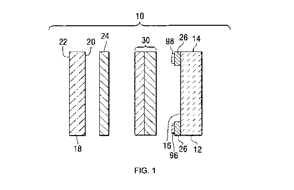
[0017] A non-limiting transparency 10 (e.g., automotive windshield)
incorporating features of
the invention is illustrated in Figure 1. The transparency 10 can have any
desired visible light,
infrared radiation, or ultraviolet radiation transmission and reflection.
For example, the
transparency 10 can have a visible light transmission of any desired amount,
e.g. greater than
0% to 100%, greater than 70%. For windshield and front sidelight areas in the
United States, the
visible light transmission is typically greater than or equal to 70%. For
privacy areas, such as rear
4
CA 03134609 2021-09-22
WO 2020/198480 PCT/US2020/024971
seat sidelights and rear windows, the visible light transmission can be less
than that for
windshields, such as less than 70%.
[0018] As seen in Figure 1, the transparency 10 includes a first ply or first
substrate 12 with a
first major surface facing the vehicle exterior, i.e. an outer major surface
14 (No. 1 surface) and
an opposed second or inner major surface 16 (No. 2 surface). The transparency
10 also includes
a second ply or second substrate 18 having an outer (first) major surface 22
(No. 4 surface) and
an inner (second) major surface 20 (No. 3 surface). This numbering of the ply
surfaces is in
keeping with conventional practice in the automotive art. The first and second
plies 12, 18 can
be bonded together in any suitable manner, such as by conventional interlayer
24. Although not
required, a conventional edge sealant can be applied to the perimeter of the
laminated
transparency 10 during and/or after lamination in any desired manner. A
decorative band, e.g.,
an opaque, translucent, or colored shade band 26, such as a ceramic band, can
be provided on
a surface of at least one of plies 12, 18, for example around the perimeter of
the inner major
surface 16 of the first ply 12. A coating 30 can be formed over at least a
portion of one of the
plies 12, 18, such as over the No. 2 surface 16 or No. 3 surface 20.
[0019] In
the non-limiting embodiment illustrated in Figure 1, the bus bar assembly
includes a
first or bottom bus bar 96 and a second or top bus bar 98 formed on the inner
surface 16 of the
outer ply 12 and separated by a bus bar to bus bar distance. The bus bars 96,
98 are in electrical
contact with the coating 30. In one non-limiting embodiment of the invention
the bus bars 96, 98
can be positioned at least partially on, or completely on, the decorative band
26, as shown in
Figure 1.
[0020] In
the broad practice of the invention, the plies 12, 18 of the transparency 10
can be of
the same or different materials. The plies 12, 18 can include any desired
material having any
desired characteristics. For example, one or more of the plies 12, 18 can be
transparent or
translucent to visible light. By "transparent" is meant having visible light
transmittance of greater
than 0% to 100%. Alternatively, one or more plies 12, 18 can be translucent.
By "translucent" is
meant allowing electromagnetic energy (e.g., visible light) to pass through
but diffusing this energy
such that objects on the side opposite the viewer are not clearly visible.
Examples of suitable
materials, but are not limited to, plastic substrates (such as acrylic
polymers, such as
polyacrylates; polyalkylmethacrylates, such as polymethylmethacrylates,
polyethylmethacrylates,
polypropylmethacrylates, and the like; polyurethanes; polycarbonates;
polyalkylterephthalates,
such as polyethyleneterephthalate (PET),
polypropyleneterephthalates,
polybutyleneterephthalate, and the like; polysiloxane-containing polymers; or
copolymers of any
monomers for preparing these, or any mixtures thereof); ceramic substrates;
glass substrates; or
CA 03134609 2021-09-22
WO 2020/198480 PCT/US2020/024971
mixtures or combinations of any of the above. For example, one or more of the
plies 12, 18 can
include conventional soda-lime-silicate glass, borosilicate glass, or leaded
glass. The glass can
be clear glass. By "clear glass" is meant non-tinted or non-colored glass.
Alternatively, the glass
can be tinted or otherwise colored glass. The glass can be annealed or heat-
treated glass. As
used herein, the term "heat- treated" means tempered or at least partially
tempered. The glass
can be of any type, such as conventional float glass, and can be of any
composition having any
optical properties, e.g., any value of visible transmission, ultraviolet
transmission, infrared
transmission, and/or total solar energy transmission. By "float glass" is
meant glass formed by a
conventional float process in which molten glass is deposited onto a molten
metal bath and
controllably cooled to form a float glass ribbon. The ribbon is then cut
and/or shaped and/or heat
treated as desired. Examples of float glass processes are disclosed in U.S.
Pat. Nos. 4,466,562
and 4,671,155. The first and second plies 12, 18 can be, for example, clear
float glass or can be
tinted or colored glass or one ply 12, 18 can be clear glass and the other ply
12, 18 colored glass.
Although not limiting to the invention, examples of glass suitable for the
first ply 12 and/or second
ply 18 are described in U.S. Pat. Nos. 4,746,347; 4,792,536; 5,030,593;
5,030,594; 5,240,886;
5,385,872; and 5,393,593. The first and second plies 12, 18 can be of any
desired dimensions,
e.g., length, width, shape, or thickness. In one exemplary automotive
transparency 10, the first
and second plies 12, 18 can each be 1 mm to 10 mm thick, e.g., 1 mm to 5 mm
thick, or 1.5 mm
to 2.5 mm, or 1.8 mm to 2.3 mm. In one non-limiting embodiment, the first ply
12 and/or the
second ply 18 can have a visible light transmittance of greater than 90%, such
as greater than
91%, at a reference wavelength of 550 nm. The glass composition for the first
ply 12 and/or
second ply 18 can have a total iron content in the range of greater than 0
weight percent (wt. %)
to 0.2 wt. % and/or a redox ratio in the range of 0.3 to 0.6.
[0021] In one non-limiting embodiment, one or both of the plies 12, 18 may
have a high visible
light transmittance at a reference wavelength of 550 nm. By "high visible
light transmittance" is
meant visible light transmittance at 550 nm greater than or equal to 85%, such
as greater than or
equal to 87%, such as greater than or equal to 90%, such as greater than or
equal to 91%, such
as greater than or equal to 92%, at 5.5 mm equivalent thickness for glass from
2 mm to 25 mm
sheet thickness. Particularly useful glass for the practice of the invention
is disclosed in U.S. Pat.
Nos. 5,030,593 and 5,030,594.
[0022] The interlayer 24 can be of any desired material and can include one or
more layers or
plies. The interlayer 24 can be a polymeric or plastic material, such as, for
example,
polyvinylbutyral (PVB), plasticized polyvinyl chloride, or multi-layered
thermoplastic materials
including polyethyleneterephthalate, etc. Suitable interlayer materials are
disclosed, for example
6
CA 03134609 2021-09-22
WO 2020/198480 PCT/US2020/024971
but not to be considered as limiting, in U.S. Pat. Nos. 4,287,107 and
3,762,988. The interlayer
24 can also be a sound absorbing or attenuating material as described, for
example, in U.S. Pat.
No. 5,796,055. The interlayer 24 can have a solar control coating provided
thereon or
incorporated therein or can include a colored material to reduce solar energy
transmission.
[0023] The coating 30 is deposited over at least a portion of a major surface
of one of the glass
plies 12, 18 such as on the inner surface 16 of the outboard glass ply 12 or
the inner surface 20
of the interior glass ply 18 (Figure 1). The coating 30 can include two
metallic films positioned
between dielectric layers applied sequentially over at least a portion of one
of the glass plies 12,
18. The coating 30 can be a heat and/or radiation reflecting coating or a
solar control coating and
can have one or more coating layers or films of the same or different
composition and/or
functionality. The coating 30 can be a multi-layer coating including two
metallic layers. Examples
of electrically conductive coatings used to make heatable windows are
disclosed in U.S. Pat. Nos.
5,653,903 and 5,028,759. Examples of solar control coatings that can be used
in the practice of
the invention are found in U.S. Pat. Nos. 4,898,789; 5,821,001; 4,716,086;
4,610,771; 4,902,580;
4,716,086; 4,806,220; 4,898,790; 4,834,857; 4,948,677; 5,059,295; and
5,028,759, and also U.S.
Pat. Appl. Publ. No. 09/058440.
[0024] Non-limiting examples of suitable coatings 30 typically include one
or more antireflective
coating films comprising dielectric or anti-reflective materials, such as
metal oxides or oxides of
metal alloys, which as transparent to visible light. The coating 30 can also
include two metallic
layers comprising a reflective metal, e.g., a noble metal such as silver or
gold, or alloys, mixtures,
or combinations thereof, and can further comprise a primer layer or barrier
film, such as titanium
or a titanium aluminum alloy, as is known in the art, located over and/or
optionally under the metal
reflective layer. The coating 30 can have one metallic layer; or can have at
least two metallic
layers. For example, the coating 30 consists of two metallic layers. In one
non-limiting
embodiment, one or more of the metallic layers can comprise silver.
[0025] Non-limiting examples of suitable materials for the primer layer
include zinc, aluminum,
vanadium, tungsten, tantalum, niobium, zirconium, manganese, chromium, tin,
nickel,
germanium, magnesium, molybdenum, silver, silicon carbon, aluminum-doped
silver, aluminum
zinc, vanadium zinc, tungsten tantalum, titanium niobium, zirconium niobium,
tungsten niobium,
aluminum niobium, aluminum titanium, tungsten titanium, tantalum titanium,
zinc titanium,
aluminum silver, zinc tin, indium zinc, silver zinc, mixtures thereof,
combinations thereof, or any
alloys thereof. The primer layer may also take the form of a metal, oxide, sub-
oxide, nitride, and/or
sub-nitride of any of the above list of materials. At least a portion of the
primer layer is an oxide
or a nitride. In certain embodiments, the primer layer is deposited in a 100%
Argon environment.
7
CA 03134609 2021-09-22
WO 2020/198480 PCT/US2020/024971
In certain embodiments, a portion of the primer layer is a nitride formed by
sputtering the metal
or metal alloy in a nitrogen (N2) atmosphere that has a specific flow rate as
to form an atmosphere
of 80% N2, with the remainder argon. The flow rate is an approximation to the
amount of N2 in
the atmosphere, but that one of ordinary skill in the art would recognize that
additional N2 may
leak into the coating chamber as the coating chamber is not hermetically
sealed from the outside
environment. In certain embodiments, a portion of the primer layer is a sub-
oxide formed by
sputtering the metal or metal alloy in an oxygen (02) atmosphere that has a
specific flow rate as
to form an atmosphere of 3% to 7% 02, with the remainder argon. The flow rate
is an
approximation to the amount of oxygen (02) in the atmosphere, but that one of
ordinary skill in
the art would recognize that additional 02 may leak into the coating chamber
as the coating
chamber is not hermetically sealed from the outside environment. The chemical
structure of the
primer material is designated by weight percent (wt. %) of an element, x. For
certain
compositions, the lower limit of one of the materials in the composition may
be "greater than 0".
When the lower limit is greater than zero (>0), the wt. % of the material is
not equal to zero but
may be any wt. % greater than 0 up to the wt. % of the upper limit. The
composition can change
before or after the layer is heated, due to reactions with atmospheric
species. These reactions
can change the wt. % distributed between the materials of the composition.
Compositions of non-
limiting examples of primer layers can be found in Table 1, where before
heating is BH and after
heating is AH. Some materials may only have only BH or AH measurements due to
that
measurement being more important for the final composition.
Table 1. Compositions of Metals for Metal Alloys Used as Primer Layers
Material Range (wt. %) Preferred Range More Preferred
Most Preferred
(wt. %) Range (wt. %)
Range (wt. %)
AlxZni_x x = >0 to 30 x = >0 to 20 x = >0 to 15 x = 1 to 12
GaxZni_x x = >0 to 20 x = >0 to 15 x = >0 to 10 x = 1 to 5
InxZni_x x = >0 to 40 x = >0 to 18 x = >0 to 15 x = 1 to 10
VxZni_x x = >0 to 20 x = >0 to 15 x = >0 to 10 x = 1 to 5
AgxZni_x x = >0 to 50 x = >0 to 40 x = >0 to 30 x = 5 to 30
x = 2 to 75 (BH) x = 2 to 60 (BH) x = 2 to 50 (BH) x = 2 to 40
(BH)
AIxTii_x x= Ito 100 (AH) x= 1 to 98 (AH) x = 2 to 95
(AH) x = 2 to 15 (AH)
x = 20 to 95 (AH)
x = 2 to 40 (BH) x = 2 to 30 (BH) x = 2 to 19 (BH) x = 2 to 13
(BH)
AlxNb1-x
x = 2 to 95 (AH) x = 2 to 80 (AH) x = 3 to 60 (AH) x = 4 to 45
(AH)
8
CA 03134609 2021-09-22
WO 2020/198480 PCT/US2020/024971
AlxNbi_x x= Ito 100 (BH) x= 1 to 98 (BH) x= 1 to 95 (BH)
x = 2 to 93 (BH)
nitride x = 1 to 100 (AH) x = 2 to 75 (AH) x = 3 to 50
(AH) x= 4 to 40 (AH)
Wxl-ii-x
sub-oxide x = 55 to 100 (BH) x = 65 to 100 (BH)
x = 75 to 100 (BH) x = 80 to 100 (BH)
(7% 02)
Wxl-ii-x
sub-oxide x = 30 to 95 (AH) x = 40 to 95 (AH)
x = 50 to 95 (AH) x = 55 to 95 (AH)
(3% 02)
x = 2 to 80 (BH) x = 2 to 60 (BH) x = 2 to 35 (BH) x= 2 to 20
TixTai_x x = 2 to 40 (AH) x = 2 to 30 (AH) x = 2 to 25
(AH) (BH and AH)
TixNbi_x x = 2 to 95 (AH) x = 2 to 93 (AH) x = 3 to 92 (AH) x = 5 to
90 (AH)
TixNbi_x x = 1 to 65 x = 1 to 50 x = 1 to 40 x = 1 to 30
nitride
x = 1 to 80 (BH) x = 1 to 70 (BH) x = 1 to 60 (BH) x = 1 to 50
(BH)
NbxZri-x
x = 60 to 100 (AH) x = 70 to 100 (AH) x = 80 to 100 (AH) x = 85 to 100
(AH)
Tax\n/i_x x = 2 to 95 (BH) x = 2 to 80 (BH) x = 3 to 60
(BH) x = 5 to 50 (BH)
x = 5 to 100 (BH) x = 6 to 90 (BH) x = 8 to 80 (BH) x = 10 to
70 (BH)
WxNbi-x
x = 2 to 50 (AH) x = 2 to 45 (AH) x = 2 to 40 (AH) x = 2 to 30
(AH)
WxNbi-x x = 2 to 90 (BH) x = 5 to 80 (BH) x = 7 to 75 (BH) x= 10 to
70 (BH)
nitride x = 2 to 70 (AH) x = 10 to 70 (AH) x = 20 to 70
(AH) x = 30 to 70 (AH)
x= 10 to 100 (BH) x =10 to 80 (BH) x= 10 to 70 (BH) x= 10 to 60
(BH)
ZnxTii-x
x = 20 to 100 (AH) x = 40 to 97 (AH) x = 50 to 94 (AH) x = 60 to 90
(AH)
[0026] The coating 30 can be deposited by any conventional method, such as but
not limited
to conventional chemical vapor deposition (CVD) and/or physical vapor
deposition (PVD)
methods. Examples of CVD processes include spray pyrolysis. Examples of PVD
processes
include electron beam evaporation and vacuum sputtering (such as magnetron
sputter vapor
deposition (MSVD)). Other coating methods could also be used, such as but not
limited to sol-
gel deposition. In one non-limiting embodiment, the coating 30 can be
deposited by MSVD.
Examples of MSVD coating devices and methods will be well understood by one of
ordinary skill
in the art and are described, for example, in U.S. Pat. Nos. 4,379,040;
4,861,669; 4,898,789;
4,898,790; 4,900,633; 4,920,006; 4,938,857; 5,328,768; and 5,492,750. In the
MSVD method,
an oxide of a metal or metal alloy can be deposited by sputtering a metal or
metal alloy containing
9
CA 03134609 2021-09-22
WO 2020/198480 PCT/US2020/024971
cathode in an oxygen containing atmosphere to deposit a metal oxide or metal
alloy oxide film on
the surface of the substrate. In one embodiment, the coating 30 is deposited
over all or
substantially all of the surface, i.e., is not deposited to form discrete
coated areas. The at least
one coating 30 can be deposited over a flat substrate and then the substrate
can be bent of
shaped in any conventional manner, such as by heating. Alternatively, the at
least one coating
30 can be deposited over a curved surface, i.e., a substrate that has already
been bent or shaped.
[0027] The invention is directed at a coating stack that has an adequately
thick total silver to
provide a visible light reflectance in the range of 8% to 50%, preferably 8%
to 30%, more
preferably 8% to 20%, most preferably 9% to 18% and an RgL* of 35 to 55,
preferably 42 to 54,
more preferably 46 to 53, or most preferably 50 to 52 to produce a neutral
color.
[0028] In one non-limiting practice of the invention, the coating provides
a visible light
reflectance of not more than 50%. For example, not more than 30%, such as not
more than 20%,
such as not more than 18%. As will be appreciated by one skilled in the art,
for laminated articles,
the reflectance is typically defined with respect to the exterior reflectance
of the laminated article.
By "exterior reflectance" is meant the reflectance of the exterior surface
(No. 1 surface 14), with
the coating 30 provided on an interior surface, such as the No. 2 surface 16
or No. 3 surface 20.
[0029] In one non-limiting practice of the invention, the coating 30
provides an exterior reflected
L* at an 8 degree angle (Rg812`) has a range of 35 to 55, preferably 40 to 54,
more preferably 46
to 53, or most preferably 50 to 52. In one non-limiting practice of the
invention, the coating 30
provides an exterior reflected color within the color space with a* at an 8
degree angle (Rg8a*) in
the range of 0 to -10. For example, in the range of-Ito -8, preferably -1.2 to
-7.0, more preferably
-1.5 to -6.8, or most preferably -1.7 to -5Ø In one non-limiting practice of
the invention, the
coating 30 provides an exterior reflected b* at an 8 degree angle (Rg8b*) in
the range of 1 to -20.
For example, in the range of 0 to -19, preferably -2.0 to -10, more preferably
-10 to -20, or most
preferably -15 to -19.
[0030] As will be appreciated by one of skill in the art, the color of an
object, and in particular
glass, is highly subjective. Observed color will depending on the lighting
conditions and
preferences of the observer. In order to evaluate color on a quantitative
basis, several color order
systems have been developed. One such method for specifying color adopted by
the
International Commission on Illumination (CIE) uses dominant wavelength (DW)
and excitation
purity (Pe). The numerical values of these two specifications for a given
color can be determined
by calculating the color coordinates x and y from the so-called tristimulus
values X, Y, Z of that
color. The color coordinates are then plotted on a 1931 CIE chromaticity
diagram and numerically
compared with the coordinates of CIE standard illuminant C, as identified in
CIE publication No.
CA 03134609 2021-09-22
WO 2020/198480 PCT/US2020/024971
15.2. This comparison provides a color space position on the diagram to
ascertain the excitation
purity and dominant wavelength of the glass color.
[0031] In another color order system, the color is specified in terms of
hue and lightness. This
system is commonly referred to as the CIELAB color system. Hue distinguishes
colors such as
red, yellow, green and blue. Lightness, or value, distinguishes the degree of
lightness or
darkness. The numerical values of these characteristics, which are identified
as L*, a* and b*,
are calculated from the tristimulus values (X, Y, Z). L* indicates the
lightness or darkness of the
color and represents the lightness plane on which the color resides. a*
indicates the position of
the color on a red (+a*) green (-a*) axis. b* indicates the color position on
a yellow (+b*) blue
(-b*) axis. When the rectangular coordinates of the CIELAB system are
converted into cylindrical
polar coordinates, the resulting color system is known as the CIELCH color
system which
specifies color in terms of lightness (L*), and hue angle (H ) and chroma
(C*). L* indicates the
lightness or darkness of the color as in the CIELAB system. Chroma, or
saturation or intensity,
distinguishes color intensity or clarity (i.e. vividness vs. dullness) and is
the vector distance from
the center of the color space to the measured color. The lower the chroma of
the color, i.e. the
less its intensity, the closer the color is to being a so-called neutral
color. With respect to the
CIELAB system, C*=(a*2+b*2)1/2. Hue angle distinguishes colors such as red,
yellow, green and
blue and is a measure of the angle of the vector extending from the a*, b*
coordinates through
the center of the CIELCH color space measured counterclockwise from the red
(+a*) axis.
[0032] It should be appreciated that color may be characterized in any of
these color systems
and one skilled in the art may calculate equivalent DW and Pe values; L*, a*,
b* values; and L*,
C*, H values from the transmittance curves of the viewed glass or composite
transparency. A
detailed discussion of color calculations is given in U.S. Pat. No. 5,792,559.
In the present
document, color is characterized using the CIELAB system (L* a* b*). However,
it is to be
understood that this is simply for ease of discussion and the disclosed colors
could be defined by
any conventional system, such as those described above.
[0033] Exemplary non-limiting coatings 30 suitable for the invention are shown
in Figures 2
and 3. This exemplary coating 30 includes two metallic layers positioned in
between dielectric
layers. It includes a base layer or a first dielectric layer 40 positioned
over or in direct contact with
at least a portion of a major surface of a substrate (e.g., the No. 2 surface
16 of the first ply 12, or
the No. 3 surface 20 of the second ply 18). A first metallic layer 48 is
positioned over or in direct
contact with at least a portion of the first dielectric layer 40. A first
primer layer 50 is positioned
over or in direct contact with at least a portion of the first metallic layer
48. A second dielectric
layer 60 is positioned over or in direct contact with the first primer layer
50. A second metallic
11
CA 03134609 2021-09-22
WO 2020/198480 PCT/US2020/024971
layer 70 is positioned over or in direct contact with at least a portion of
the second dielectric layer
60. A second primer layer 72 may be positioned over or in direct contact with
the second metallic
layer 70. A third dielectric layer 80 is positioned over or in direct contact
with the second primer
layer 72. An outermost protective layer 100 may be positioned over or in
direct contact with the
third dielectric layer 80.
[0034] The dielectric layers can comprise one or more films of antireflective
materials and/or
dielectric materials, such as, but not limited to metal oxides, oxides of
metal alloys, nitrides,
oxynitrides, or mixtures thereof. The first dielectric layer 40 can be
transparent to visible light.
Examples of suitable metal oxides for the first dielectric layer 40 include
oxides of titanium,
hafnium, zirconium, niobium, zinc, bismuth, lead, indium, tin, magnesium,
gallium, vanadium,
aluminum, silicon, alloys thereof, mixtures thereof, or combinations thereof.
These metal oxides
can have small amount of other materials, such as manganese in bismuth oxide,
tin in indium
oxide, etc. Alternatively, oxides or metal alloys or metal mixtures, such as
oxides containing zinc
and tin (e.g., zinc stannate); oxides of indium-tin alloys; silicon nitrides;
silicon aluminum nitrides;
or aluminum nitrides can be used. Further, doped metal oxides, such as
aluminum-doped zinc
oxide, antimony-doped tin oxide, nickel or boron-doped silicon oxides, gallium-
doped zinc oxide,
indium-doped zinc oxide, magnesium-doped zinc oxide, vanadium-doped zinc
oxide, indium-
doped tin oxides, or mixtures thereof can be used. In one non-limiting
embodiment, the first film
of the first dielectric layer 42 can be a zinc/tin alloy oxide formed over at
least a portion of the
substrate (e.g., the No. 2 surface 16 of the first ply 12, or the No. 3
surface 20 of the second ply
18). The zinc/tin alloy oxide can be obtained from MSVD from a cathode of zinc
and tin that can
comprise zinc and tin in proportions of 10 wt. % to 90 wt. % zinc and 90 wt. %
to 10 wt. % tin.
One suitable metal alloy oxide that can be present in the first film of the
first dielectric layer 42 is
zinc stannate. By "zinc stannate" is meant a composition of ZnxSni_x02_x
(Formula 1) where "x"
varies in the range of greater than 0 to less than 1. For instance, "x" can be
greater than 0 and
can be any fraction or decimal between greater than 0 to less than 1. For
example, where x=2/3,
Formula 1 is Zn2/3Sn1/304/3, which is more commonly described at Zn2SnO4. A
zinc stannate
containing film has one or more of the forms of Formula 1 in a predominant
amount in the film.
[0035] The second film of the first dielectric layer 44 is formed over at
least a portion of the first
film of the first dielectric layer 42 and can comprise zinc oxide, silicon
nitride, aluminum-doped
zinc oxide, gallium doped-zinc oxide, indium-doped zinc oxide, magnesium-doped
zinc oxide,
vanadium-doped zinc oxide, or indium-doped tin oxide, mixtures or combinations
thereof. In one
non-limiting embodiment, the second film of the first dielectric layer 44 can
be a zinc-containing
film, such as zinc oxide. The zinc oxide film can be deposited from a zinc
cathode that includes
12
CA 03134609 2021-09-22
WO 2020/198480 PCT/US2020/024971
other materials to improve the sputtering characteristics of the cathode. For
example, the zinc
cathode can include a small amount (e.g., less than 10 wt. %, such as greater
than 0 to 5 wt. %)
of tin to improve sputtering. In which case, the resultant zinc oxide film
would include a small
percentage of tin oxide, e.g., 0 to less than 10 wt. % tin oxide, e.g., 0 to 5
wt. % tin oxide. An
oxide layer sputtered from a zinc/tin cathode having 95 wt. % zinc and 5 wt. %
tin, or preferably
90 wt. % zinc and 10 wt. % tin, is referred to as a zinc oxide film. The small
amount of tin in the
cathode (e.g., less than 10 wt. %) is believed to form a small amount of tin
oxide in the
predominately zinc oxide-containing second film of the first dielectric layer
44.
[0036] In an exemplary non-limiting embodiment, the second film 44 is a
film consisting of at
least one of the following: aluminum-doped zinc oxide, gallium doped-zinc
oxide, indium-doped
zinc oxide, magnesium-doped zinc oxide, vanadium-doped zinc oxide, or indium-
doped tin oxide.
The aluminum-doped zinc oxide, gallium doped-zinc oxide, indium-doped zinc
oxide, magnesium-
doped zinc oxide, vanadium-doped zinc oxide, or indium-doped tin oxide film is
deposited from a
zinc cathode that includes other materials to improve the sputtering
characteristics of the cathode.
For example, the aluminum-doped zinc oxide, gallium doped-zinc oxide, indium-
doped zinc oxide,
magnesium-doped zinc oxide, vanadium-doped zinc oxide, or indium-doped tin
oxide film can
include a small amount (e.g., less than 10 wt. %, such as greater than 0 to 5
wt. %) of tin to
improve sputtering. In which case, the resultant aluminum-doped zinc oxide,
gallium doped-zinc
oxide, indium-doped zinc oxide, magnesium-doped zinc oxide, vanadium-doped
zinc oxide, or
indium-doped tin oxide film would include a small percentage of tin oxide,
e.g., 0 wt. % to less
than 10 wt. % tin oxide, e.g., 0 wt. % to 5 wt. % tin oxide.
[0037] One non-limiting embodiment is in which the first film of the first
dielectric layer 42 is
zinc stannate and the second film of the first dielectric layer 44 comprises
zinc oxide, silicon
nitride, aluminum-doped zinc oxide, gallium doped-zinc oxide, indium-doped
zinc oxide,
magnesium-doped zinc oxide, vanadium-doped zinc oxide, or indium-doped tin
oxide over at least
a portion of the first film of the first dielectric layer 42.
[0038] The first dielectric layer 40 can have a total thickness in the range
of 10 nm to 55 nm,
preferably 20 nm to 53 nm, more preferably 25 nm to 50 nm, most preferably 29
nm to 48 nm.
[0039] In one non-limiting embodiment, the first dielectric layer 40
comprises a first seed film
in direct contact with the first metallic layer 48, not depicted in the
figures. The seed film can
comprise aluminum, aluminum silver, aluminum zinc, zinc, zinc tin, germanium,
nickel,
magnesium, silicon carbide, aluminum nitride, indium zinc, vanadium zinc,
gallium zinc, indium
tin, niobium, zirconium, tantalum, molybdenum, aluminum-doped silver, silver,
silver zinc, titanium
aluminum, alloys thereof, mixtures thereof, oxides thereof, sub-oxides
thereof, nitrides thereof,
13
CA 03134609 2021-09-22
WO 2020/198480 PCT/US2020/024971
sub-nitrides thereof, or combinations thereof. In one non-limiting embodiment,
the seed film can
comprise aluminum zinc, vanadium zinc, zinc, silver zinc, metals thereof,
alloys thereof, oxides
thereof, or sub-oxides thereof. In another embodiment, the seed film can
comprise gallium zinc,
indium zinc, indium tin, metals thereof, alloys thereof, oxides thereof, or
sub-oxides thereof.
Compositions of non-limiting examples of the seed film can be found in Table
2. In certain
embodiments, a portion of the seed film is formed in an 02 atmosphere that has
a specific flow
rate as to form an atmosphere of 1% to 70% 02, with the remainder argon. The
flow rate is an
approximation to the amount of 02 in the atmosphere, but that one of ordinary
skill in the art would
recognize that additional 02 may leak into the coating chamber as the coating
chamber is not
hermetically sealed from the outside environment. In one embodiment, the seed
film comprises
VxZni_x oxide. In another embodiment, the seed film comprises AlxZni_x oxide.
In another
embodiment, the seed film comprises GaxZni_x oxide. In another embodiment, the
seed film
comprises InxZni_x oxide. In another embodiment, the seed film comprises
SnxIni_x oxide. In
another embodiment, the seed film comprises Ag deposited in an oxygen/argon
gas environment.
In another embodiment, the seed film comprises AlxAgi_x. In one non-limiting
embodiment, the
second film of the first dielectric layer 44 is the seed film. In some
embodiments, the first dielectric
layer 40 comprises a first film 42, a second film 44, and a seed film. The
seed film can have a
total thickness in the range of 0.5 nm to 10 nm, preferably 0.75 nm to 8 nm,
more preferably 0.9
nm to 6 nm.
Table 2. Compositions of Metals for Metal Alloys Used as Seed Films
Material Range (wt. %) Preferred Range More Preferred Most
Preferred
(wt. %) Range (wt. %)
Range (wt. %)
Ag x = 1 to 70 % gas x = 1 to 50 % gas x = 10 to 40 % gas x = 20 to
40 % gas
deposited in flow flow flow flow
02 gas
environment
AlxAgi_x x = Ito 35 x = 1 to 20 (BH x = Ito 18 x = Ito 15
oxide (BH and AH) and AH) (BH and AH) (BH and AH)
AlxZni_x x = 1 to 25 x = 1 to 15 x = 1 to 12 x = 1 to 10
oxide
GaxZni_x x = 1 to 20 x = 1 to 15 x = 1 to 10 x = 1 to 5
oxide
14
CA 03134609 2021-09-22
WO 2020/198480 PCT/US2020/024971
SnxIni_x x = 1 to 20 x = 2 to 18 x = 4 to 15 x = 5 to 12
oxide
VxZni-x x = 1 to 25 x = 1 to 15 x = 1 to 10 x = 1 to 8
oxide
[0040] A first metallic layer 48 can be deposited over at least a portion of
the first dielectric
layer 40. The first metallic layer 48 can include a reflective metal, such as
but not limited to
metallic gold, silver, mixtures thereof, alloys thereof, or combinations
thereof. In one embodiment,
the first metallic layer 48 comprises a metallic silver layer. The first
metallic layer 48 can have a
total thickness in the range of 5 nm to 20 nm, preferably 7.5 nm to 15 nm,
more preferably 9 nm
to 14 nm, most preferably 9.7 to 13.3 nm.
[0041] A first primer layer 50 may be deposited over at least a portion of the
first metallic layer
48. The first primer layer 50 can be an oxygen-capturing material, such as
titanium, that can be
sacrificial during the deposition process to prevent degradation or oxidation
of the first metallic
layer 48 during the sputtering process or subsequent heating processes. The
oxygen-capturing
material can be chosen to oxidize before the material of the first metallic
layer 48. Examples of
materials suitable for the primer layer include zinc, aluminum, vanadium,
tungsten, tantalum,
niobium, zirconium, manganese, chromium, tin, nickel, germanium, magnesium,
molybdenum,
silver, silicon carbon, aluminum-doped silver, aluminum zinc, vanadium zinc,
tungsten tantalum,
titanium niobium, zirconium niobium, tungsten niobium, aluminum niobium,
aluminum titanium,
tungsten titanium, tantalum titanium, zinc titanium, aluminum silver, zinc
tin, indium zinc, silver
zinc, mixtures thereof, combinations thereof, or any alloys thereof, where the
primer is deposited
as a metal and subsequently oxidized. Examples of suitable materials for the
first primer layer 50
can be found in Table 1. At least a portion of the primer layer is a nitride
or an oxide. If silver zinc,
zinc, silver zinc oxide, titanium, aluminum zinc oxide, indium zinc oxide,
gallium zinc oxide, or
vanadium zinc oxide is used as the first primer layer 50, it would preferably
oxidize before
oxidation of the underlying metallic layer. In one embodiment, the first
primer layer 50 is titanium.
In another embodiment, the first primer layer 50 comprises silver zinc. In
another embodiment,
the first primer layer 50 comprises zinc. In another embodiment, the first
primer layer 50
comprises AgxZni_x. In another embodiment, the first primer layer 50 comprises
AgxZni_x oxide.
In another embodiment, the first primer layer 50 comprises AlxZni_x oxide.
In another
embodiment the first primer layer 50 comprises InxZni_x oxide. In another
embodiment, the first
primer layer 50 comprises GaxZni_x oxide. In another embodiment, the first
primer layer 50
comprises VxZni_x oxide. In another embodiment, the first primer layer 50
comprises AIxTii_x oxide.
CA 03134609 2021-09-22
WO 2020/198480 PCT/US2020/024971
In another embodiment, the first primer layer 50 comprises AI,Nbi_x oxide. In
another
embodiment, the first primer layer 50 comprises AlxNbi_x nitride. In another
embodiment, the first
primer layer 50 comprises WxNbi_x nitride. In another embodiment, the first
primer layer 50
comprises WxTii_x oxide. In another embodiment, the first primer layer 50
comprises TixTai_x
oxide. In another embodiment, the first primer layer 50 comprises TixNbi_x
oxide. In another
embodiment, the first primer layer 50 comprises TixNbi_x nitride. In another
embodiment, the first
primer layer 50 comprises NbxZri_x oxide. In another embodiment, the first
primer layer 50
comprises TaxWi_x oxide. In another embodiment, the first primer layer 50
comprises WxNbi_x
oxide. In another embodiment, the first primer layer 50 comprises ZnxTii_x
oxide. The first primer
layer 50 has a total thickness in the range of 0.5 nm to 10 nm, preferably 1.0
nm to 5.0 nm, more
preferably 1.0 to 2.5 nm.
[0042] A second dielectric layer 60 can be deposited over at least a portion
of the first metallic
layer 48 or the optional first primer layer 50. The second dielectric layer 60
can include one or
more materials discussed above with respect to the first dielectric layer. In
the illustrated non-
limiting example of Figure 2, the second dielectric layer 60 includes a first
film of the second
dielectric layer 62 deposited over the first metallic layer 48 or the optional
first primer layer 50.
The first film of the second dielectric layer 62 comprises an oxide, a
nitride, an oxynitride, or a
mixture thereof of a metal selected from the group consisting of titanium,
hafnium, zirconium,
niobium, zinc, bismuth, lead, indium, tin, silicon, magnesium, gallium,
vanadium, aluminum, alloys
thereof, mixtures thereof, or combinations thereof. In one embodiment the
first film of the second
dielectric layer 62 comprises zinc oxide. In another embodiment, the first
film of the second
dielectric layer 62 comprises aluminum-doped zinc oxide. In another
embodiment, the first film
of the second dielectric layer 62 comprises indium-doped zinc oxide. In
another embodiment, the
first film of the second dielectric layer 62 comprises gallium-doped zinc
oxide. In another
embodiment, the first film of the second dielectric layer 62 comprises indium-
doped tin oxide. In
another embodiment, the first film of the second dielectric layer 62 comprises
vanadium-doped
zinc oxide.
[0043] The second film of the second dielectric layer 64 can be deposited over
at least a portion
of the first film of the second dielectric layer 62. The second film of the
second dielectric layer 64
comprises an oxide, a nitride, an oxynitride, or a mixture therefore of a
metal selected from the
group consisting of titanium, hafnium, zirconium, niobium, zinc, bismuth,
lead, indium, tin, silicon,
magnesium, gallium, vanadium, aluminum, alloys thereof, mixtures thereof, or
combinations
thereof. In one non-limiting embodiment, the second film of the second
dielectric layer 64 is zinc
stannate.
16
CA 03134609 2021-09-22
WO 2020/198480 PCT/US2020/024971
[0044] A third film of the second dielectric layer 66 can be deposited over at
least a portion of
the second film of the second dielectric layer 64. The third film of the
second dielectric layer 66
can comprise comprises an oxide, a nitride, an oxynitride, or a mixture
therefore of a metal
selected from the group consisting of titanium, hafnium, zirconium, niobium,
zinc, bismuth, lead,
indium, tin, silicon, magnesium, gallium, vanadium, aluminum, alloys thereof,
mixtures thereof, or
combinations thereof. The third film of the second dielectric layer 66 can
comprise aluminum-
doped zinc oxide, gallium doped-zinc oxide, indium-doped zinc oxide, magnesium-
doped zinc
oxide, vanadium-doped zinc oxide, or indium-doped tin oxide, or mixtures
thereof. In one
embodiment, the third film of the second dielectric layer 66 comprises zinc
oxide. In another
embodiment, the third film of the second dielectric layer 66 comprises indium-
doped zinc oxide.
In another embodiment, the third film of the second dielectric layer 66
comprises gallium-doped
zinc oxide. In another embodiment, the third film of the second dielectric
layer 66 comprises
indium-doped tin oxide. In another embodiment, the third film of the second
dielectric layer 66
comprises vanadium-doped zinc oxide. In another embodiment, the first
dielectric layer 40 or the
second dielectric layer 60 comprises a silicon nitride film.
[0045] One non-limiting embodiment is in which the first film of the second
dielectric layer 62
comprises zinc oxide, the second film of the second dielectric layer 64
comprises zinc stannate,
and the third film of the second dielectric layer 66 comprises zinc oxide,
silicon nitride, aluminum-
doped zinc oxide, gallium doped-zinc oxide, indium-doped zinc oxide, magnesium-
doped zinc
oxide, vanadium-doped zinc oxide, or indium-doped tin oxide over at least a
portion of the second
film of the second dielectric layer 44.
[0046] The second dielectric layer 60 can have a total thickness in the range
of 50 nm to 150
nm, preferably 75 nm to 125 nm, more preferably 90 nm to 110 nm, most
preferably 93 nm to 100
nm.
[0047] In one non-limiting embodiment, the second dielectric layer 60
comprises a seed film
positioned in direct contact with the second metallic layer 70. The seed film
can include one or
more materials discussed above with respect to the seed film of the first
dielectric layer and Table
2. The seed film can comprise aluminum, aluminum silver, aluminum zinc, zinc,
zinc tin,
germanium, nickel, magnesium, silicon carbide, aluminum nitride, indium zinc,
vanadium zinc,
gallium zinc, indium tin, niobium, zirconium, tantalum, molybdenum, aluminum-
doped silver,
silver, silver zinc, titanium aluminum, alloys thereof, mixtures thereof,
oxides thereof, sub-oxides
thereof, nitrides thereof, sub-nitrides thereof, or combinations thereof. In
one non-limiting
embodiment, the seed film can comprise aluminum zinc, vanadium zinc, zinc,
silver zinc, metals
thereof, alloys thereof, oxides thereof, or sub-oxides thereof. In another
embodiment, the seed
17
CA 03134609 2021-09-22
WO 2020/198480 PCT/US2020/024971
film can comprise gallium zinc, indium zinc, indium tin, metals thereof,
alloys thereof, oxides
thereof, or sub-oxides thereof. In one embodiment, the seed film comprises
VxZni_x oxide. In
another embodiment, the seed film comprises AlxZni_x oxide. In another
embodiment, the seed
film comprises GaxZni_x oxide. In another embodiment, the seed film comprises
InxZni_x oxide. In
another embodiment, the seed film comprises SnxIni_x oxide. In another
embodiment, the seed
film comprises Ag deposited in an oxygen/argon gas environment. In another
embodiment, the
seed film comprises AlxAgi_x. In some embodiments, the second dielectric layer
60 has a first film
62, a second film 64, and a seed film. In some embodiments, the second
dielectric layer 60 has
a first film 62, a second film 64, a third film 66, and a seed film. The seed
film can have a total
thickness in the range of 0.5 nm to 10 nm, preferably 0.75 nm to 8 nm, more
preferably 0.9 nm to
6 nm.
[0048] A second metallic layer 70 can be deposited over at least a portion of
the second
dielectric layer 60. The second metallic layer 70 can include any one or more
of the reflective
materials described above with respect to the first metallic layer 48. In one
non-limiting
embodiment, the second metallic layer 70 comprises silver. The second metallic
layer 70 can
have a total thickness in the range of 5 nm to 20 nm, preferably 5 nm to 15
nm, more preferably
7.5 nm to 12.5 nm, most preferably 7.5 nm to 10.3 nm.
[0049] A second primer layer 72 can be deposited over at least a portion of
the second metallic
layer 70. The second primer layer 72 can be any of the materials described
above with respect
to the first primer layer 50 and Table 1. In one non-limiting embodiment, the
second primer layer
72 comprises titanium. In another embodiment, the second primer layer 72
comprises silver zinc.
In another embodiment, the second primer layer 72 comprises zinc. In another
embodiment, the
second primer layer 72 comprises AgxZni_x. In another embodiment, the second
primer layer 72
comprises AgxZni_x oxide. In another embodiment, the second primer layer 72
comprises AlxZni_
x oxide. In another embodiment, the second primer layer 72 comprises InxZni_x
oxide. In another
embodiment, the second primer layer 72 comprises GaxZni_x oxide. In another
embodiment, the
second primer layer 72 comprises VxZni_x oxide. In another embodiment, the
second primer layer
72 comprises AIxTii_x oxide. In another embodiment, the second primer layer 72
comprises AlxNbi_
x oxide. In another embodiment, the second primer layer 72 comprises AlxNbi_x
nitride. In another
embodiment, the second primer layer 72 comprises WxNbi_x nitride. In another
embodiment, the
second primer layer 72 comprises WxTii_x oxide. In another embodiment, the
second primer layer
72 comprises TixTai_x oxide. In another embodiment, the second primer layer 72
comprises
TixNbi_x oxide. In another embodiment, the second primer layer 72 comprises
TixNbi_x nitride. In
another embodiment, the second primer layer 72 comprises NbxZri_x oxide. In
another
18
CA 03134609 2021-09-22
WO 2020/198480 PCT/US2020/024971
embodiment, the second primer layer 72 comprises TaxWi_x oxide. In another
embodiment, the
second primer layer 72 comprises WxNbi_x oxide. In another embodiment, the
second primer
layer 72 comprises ZnxTii_x oxide. The second primer layer 72 has a total
thickness in the range
of 0.5 nm to 10 nm, preferably 1.0 nm to 5 nm, more preferably 1.0 nm to 2.5
nm.
[0050] A third dielectric layer 80 can be deposited over at least a portion of
the second metallic
layer 70 or the second primer layer 72. The third dielectric layer 80 can also
include one or more
materials discussed above with respect to the first and second dielectric
layers. In one non-
limiting embodiment, the third dielectric layer 80 comprises a first film of
the third dielectric layer
82. The first film of the third dielectric layer 82 comprises an oxide, a
nitride, an oxynitride, or a
mixture therefore of a metal selected from the group consisting of titanium,
hafnium, zirconium,
niobium, zinc, bismuth, lead, indium, tin, silicon, magnesium, gallium,
vanadium, aluminum, alloys
thereof, mixtures thereof, or combinations thereof. In one embodiment, the
first film of the third
dielectric layer 82 comprises zinc oxide. In another non-limiting embodiment,
the first film of the
third dielectric layer 82 comprises zinc stannate. In another embodiment, the
first film of the third
dielectric layer 82 comprises aluminum-doped zinc oxide. In another
embodiment, the first film
of the third dielectric layer 82 comprises indium-doped zinc oxide. In another
embodiment, the
first film of the third dielectric layer 82 comprises gallium-doped zinc
oxide. In another
embodiment, the first film of the third dielectric layer 82 comprises indium-
doped tin oxide. In
another embodiment, the first film of the third dielectric layer 82 comprises
vanadium-doped zinc
oxide.
[0051] A second film of the third dielectric layer 84 can be deposited over at
least a portion of
the first film of the third dielectric layer 82. The second film of the third
dielectric layer 84
comprises an oxide, a nitride, an oxynitride, or a mixture thereof of a metal
selected from the
group consisting of titanium, hafnium, zirconium, niobium, zinc, bismuth,
lead, indium, tin, silicon,
magnesium, gallium, vanadium, aluminum, alloys thereof, mixtures thereof, or
combinations
thereof. The second film of the third dielectric layer 84 can comprise
aluminum-doped zinc oxide,
gallium doped-zinc oxide, indium-doped zinc oxide, magnesium-doped zinc oxide,
vanadium-
doped zinc oxide, or indium-doped tin oxide, or mixtures thereof. In one
embodiment, the second
film of the third dielectric layer 84 comprises zinc oxide. In one embodiment,
the second film of
the third dielectric layer 84 comprises zinc stannate. In another embodiment,
the second film of
the third dielectric layer 84 comprises silicon nitride or silicon oxynitride.
In another embodiment,
the second film of the third dielectric layer 84 comprises indium-doped zinc
oxide. In another
embodiment, the second film of the third dielectric layer 84 comprises gallium-
doped zinc oxide.
In another embodiment, the second film of the third dielectric layer 84
comprises indium-doped
19
CA 03134609 2021-09-22
WO 2020/198480 PCT/US2020/024971
tin oxide. In another embodiment, the second film of the third dielectric
layer 84 comprises
vanadium-doped zinc oxide.
[0052] An optional third film of the third dielectric layer can be deposited
over at least a portion
of the second film of the third dielectric layer 84. The optional third film
of the third dielectric layer
can comprise an oxide, a nitride, an oxynitride, or a mixture thereof of a
metal selected from the
group consisting of titanium, hafnium, zirconium, niobium, zinc, bismuth,
lead, indium, tin, silicon,
magnesium, gallium, vanadium, aluminum, alloys thereof, mixtures thereof, or
combinations
thereof. The third film of the third dielectric layer can comprise aluminum-
doped zinc oxide,
gallium doped-zinc oxide, indium-doped zinc oxide, magnesium-doped zinc oxide,
vanadium-
doped zinc oxide, or indium-doped tin oxide, or mixtures thereof. In one non-
limiting embodiment,
the optional third film of the third dielectric layer comprises zinc oxide. In
another embodiment,
the third film of the third dielectric layer comprises indium-doped zinc
oxide. In another
embodiment, the third film of the third dielectric layer comprises gallium-
doped zinc oxide. In
another embodiment, the third film of the third dielectric layer comprises
indium-doped tin oxide.
In another embodiment, the third film of the third dielectric layer comprises
vanadium-doped zinc
oxide. In another embodiment, the optional third film of the third dielectric
layer comprises silicon
nitride or silicon oxynitride. In another embodiment, the optional third film
of the third dielectric
layer comprises titanium oxide.
[0053] One non-limiting embodiment is in which the first film of the third
dielectric layer 82
comprises zinc oxide or zinc stannate, and the second film of the third
dielectric layer 84
comprises zinc oxide, zinc stannate, silicon nitride, aluminum-doped zinc
oxide, gallium doped-
zinc oxide, indium-doped zinc oxide, magnesium-doped zinc oxide, vanadium-
doped zinc oxide,
or indium-doped tin oxide over at least a portion of the first film of the
third dielectric layer 82.
[0054] The third dielectric layer 80 can have a total thickness in the range
of 20 nm to 75 nm,
preferably 25 nm to 50 nm, more preferably 30 nm to 45 nm, most preferably 36
nm to 41 nm.
[0055] In one non-limiting embodiment, the coated article comprises a first
and a second
metallic layer 48, 70. There are no additional metallic layers in the coated
article. The metallic
layers may include only silver or only silver and gold.
[0056] Each metallic layer has a thickness. In one non-limiting embodiment,
the total combined
thickness of the metallic layers is in the range of 10 nm to 30 nm, preferably
12 nm to 25 nm,
most preferably 15 nm to 22 nm, most preferably 16 nm to 18 nm.
[0057] The coating can include an outermost protective layer 100, which, for
example in the
non-limiting embodiment shown in Figure 2, is deposited over at least a
portion of the third
dielectric layer 80, to assist in protecting the underlying layers, such as
the metallic layers, from
CA 03134609 2021-09-22
WO 2020/198480 PCT/US2020/024971
mechanical and chemical attack during processing. The outermost protective
layer 100 can be
an oxygen barrier coating layer to prevent or reduce the passage of ambient
oxygen into the
underlying layers of the coating 30, such as during heating or bending. The
outermost protective
layer 100 can be of any desired material or mixture of materials and can be
comprised of one or
more protective films. In one exemplary embodiment, the outermost protective
layer 100 can
include a single layer comprising one or more metal oxide materials, such as
but not limited to
oxides of aluminum, silicon, or mixtures thereof. For example, the outermost
protective coating
100 can be a single coating layer comprising in the range of 0 wt. % to 100
wt. % alumina and/or
100 wt. % to 0 wt. % silica, such as 5 wt. % to 95 wt. % alumina and 95 wt. %
to 5 wt. % silica,
such as 10 wt. % to 90 wt. % alumina and 90 wt. % to 10 wt. % silica, such as
15 wt. % to 90 wt.
% alumina and 85 wt. % to 10 wt. % silica, such as 50 wt. % to 75 wt. %
alumina and 50 wt. % to
25 wt. % silica, such as 50 wt. % to 70 wt. % alumina and 50 wt. % to 30 wt. %
silica, such as 35
wt. % to 100 wt. % alumina and 65 wt. % to 0 wt. % silica, such as 70 wt. % to
90 wt. % alumina
and 30 wt. % to 10 wt. % silica, e.g., 75 wt. % to 85 wt. % alumina and 25 wt.
% to 15 wt. % silica,
e.g., 88 wt. % alumina and 12 wt. % silica, e.g., 65 wt. % to 75 wt. % alumina
and 35 wt. % to 25
wt. % silica, e.g., 70 wt. % alumina and 30 wt. % silica, e.g., 60 wt. % to
less than 75 wt. % alumina
and greater than 25 wt. % to 40 wt. % silica. Other materials, such as
aluminum, chromium,
hafnium, yttrium, nickel, boron, phosphorous, titanium, zirconium, and/or
oxides thereof can also
be present, such as to adjust the refractive index of the outermost protective
layer 100. In one
non-limiting embodiment, the refractive index of the outermost protective
layer 100 can be in the
range of 1 to 3, such as 1 to 2, such as 1.4 to 2, such as 1.4 to 1.8.
[0058] In one non-limiting embodiment, the protective later 100 is a
combination silica and
alumina coating. The outermost protective layer 100 can be sputtered from two
cathodes (e.g.,
one silicon and one aluminum) or from a single cathode containing both silicon
and aluminum.
This silicon aluminum oxide outermost protective layer 100 can be written as
SixAli_x00.5,02,
where x can vary from greater than 0 to less than 1. In one exemplary
embodiment, the outermost
protective layer 100 comprises 15 wt. % alumina and 85 wt. % silica. In
another embodiment, the
outermost protective coating 100 comprises SiO2, A1203, SiA10, alloys thereof,
and mixtures
thereof.
[0059] In one non-limiting embodiment, the outermost protective layer 100 may
be comprised
of silicon nitride (Si3N4), silicon oxynitride (SiON), silicon aluminum
nitride (SiAIN), silicon
aluminum oxynitride (SiAION), a mixture thereof, and/or an alloy thereof and
which may provide
increased durability to the coated article. The outermost protective layer 100
may be formed of
silicon nitride deposited with other materials having superior electrical
conductivity to improve
21
CA 03134609 2021-09-22
WO 2020/198480 PCT/US2020/024971
sputtering of the silicon. For example, during deposition, the silicon cathode
can include a small
amount (e.g., up to 20 wt. %, up to 15 wt. %, up to 10 wt. %, or up to 5 wt.
%) of aluminum to
improve sputtering. In which case, the resultant silicon nitride layer would
include a small
percentage of aluminum, e.g., up to 15 wt. % aluminum, e.g., up to 10 wt. %
aluminum, e.g., up
to 5 wt. % aluminum. A coating layer deposited from a silicon cathode having
up to 10 wt. %
aluminum (added to enhance the conductivity of the cathode) is referred to
herein as a "silicon
nitride" layer, even though a small amount of aluminum may be present. The
small amount of
aluminum in the cathode (e.g., less than or equal to 15 wt. %, such as less
than or equal to 10 wt.
%, such as less than or equal to 5 wt. %) is believed to form aluminum nitride
in the predominately
silicon nitride outermost protective layer 100. The outermost protective layer
100 may be formed
in a nitrogen atmosphere; however, it is to be understood that other gasses,
such as oxygen, may
be present in the atmosphere during the deposition of the outermost protective
layer 100.
[0060] In another non-limiting embodiment, the outermost protective layer 100
can be a
multilayer coating comprising a first protective film and a second protective
film formed over at
least a portion of the first protective film. The first protective film can
comprise alumina, silica,
titania, zirconia, tin oxide, mixtures thereof, or an alloy thereof. In one
specific non-limiting
embodiment, the first protective film can comprise alumina or an alloy
comprising alumina and
silica. For example, the first protective film can comprise a silica/alumina
mixture having greater
than 5 wt. % alumina, such as greater than 10 wt. % alumina, such as greater
than 15 wt. %
alumina, such as 50 wt. % to 70 wt. % alumina, such as in the range of 60 wt.
% to 100 wt. %
alumina and 40 wt. % to 0 wt. % silica, e.g., 60 wt. % alumina and 40 wt. %
silica. In another
example, the first protective film can comprise zinc stannate. In another
example, the first
protective film can comprise zirconia.
[0061] The second protective film may comprise, for example, a metal oxide or
metal nitride.
The second protective film can be titania, alumina, silica, zirconia, tin
oxide, a mixture thereof, or
an alloy thereof. For example, the second protective film can comprise a
titania/alumina mixture
having 40-60 wt. % alumina and 60-40 wt. % titania; 45-55 wt. % alumina and 55-
45 wt. % titania;
48-52 wt. % alumina and 52-48 wt. % titania; 49-51 wt. % alumina and 51-49 wt.
% titania; or 50
wt. % alumina and 50 wt. % titania. An example of the second protective film
may include titanium
aluminum oxide (TiA10). Another example of the second protective film is a
silica/alumina mixture
having greater than 40 wt. % silica, such as greater than 50 wt. % silica,
such as greater than 60
wt. % silica, such as greater than 70 wt. % silica, such as greater than 80
wt. % silica, such as in
the range of 80 wt. % to 90 wt. % silica and 10 wt. % to 20 wt. % alumina,
e.g., 85 wt. % silica
and 15 wt. % alumina.
22
CA 03134609 2021-09-22
WO 2020/198480 PCT/US2020/024971
[0062] In non-limiting examples, the outermost protective layer 100 may
include an additional
third protective film formed over at least a portion of the second protective
film. The third
protective film can be any of the materials used to form the first and second
protective films. The
third protective film, for example, can comprise alumina, silica, titania,
zirconia, tin oxide, or
mixtures thereof. For example, the third protective film can comprise a
mixtures of silica and
alumina. In another example, the third protective film comprises alumina and
titania. In another
example, the third protective film comprises zirconia.
[0063] The outermost protective layer 100 is the outermost layer of the coated
article. Further,
the outermost protective layer 100 can be of non-uniform thickness. By "non-
uniform thickness"
is meant that the thickness of the outermost protective layer 100 can vary
over a given unit area,
e.g., the outermost protective layer 100 can have high and low spots or areas.
Non-limiting
examples of suitable protective layers are described in U.S. Pat. Application
Nos. 10/007,382;
10/133,805; 10/397,001; 10/422,095; and 10/422,096.
[0064] The outermost protective layer 100 can have a total thickness in the
range of 20 nm to
120 nm, preferably 25 nm to 110 nm, more preferably 30 nm to 100 nm, most
preferably 35 nm
to 90 nm.
[0065] The invention is further described in the following numbered clauses:
[0066] Clause 1. A coated article comprising a substrate; a functional coating
applied over at
least a portion of the substrate, the functional coating comprising a first
dielectric layer over at
least a portion of the substrate; a first metallic layer over at least a
portion of the first dielectric
layer; a first primer layer over at least a portion of the first metallic
layer; a second dielectric layer
over at least a portion of the first primer layer; a second metallic layer
over at least a portion of
the second dielectric layer; a second primer layer over at least a portion of
the second metallic
layer; and a third dielectric layer over at least a portion of the second
primer layer; wherein the
coated article has a RgL* value is at least 35, and no more than 55.
[0067] Clause 2. The coated article of clause 1, wherein the RgL* value is at
least 42.
[0068] Clause 3. The coated article of clause 1, wherein the RgL* value is no
more than 52.
[0069] Clause 4. The coated article of any of the preceding clauses, wherein
at least one of
the metallic layers comprises at least one of silver, gold, mixtures thereof,
or alloys thereof.
[0070] Clause 5. The coated article of any of the preceding clauses, wherein
at least one of
the metallic layers comprise metallic silver.
[0071] Clause 6. The coated article of any of the preceding clauses, wherein
the first metallic
layer comprises a total thickness of 5 nm to 20 nm, preferably 7.5 nm to 15
nm, more preferably
9 nm to 14 nm, most preferably 9.7 nm to 13.3 nm.
23
CA 03134609 2021-09-22
WO 2020/198480 PCT/US2020/024971
[0072] Clause 7. The coated article of any of the preceding clauses, wherein
the second
metallic layer comprises a total thickness of 5 nm to 20 nm, preferably 5 nm
to 15 nm, more
preferably 7.5 nm to 12.5 nm, most preferably 7.5 nm to 10.3 nm.
[0073] Clause 8. The coated article of clause 1, wherein at least one of the
dielectric layers
comprise zinc stannate, zinc oxide, silicon nitride, aluminum-doped zinc
oxide, gallium doped-
zinc oxide, indium-doped zinc oxide, magnesium-doped zinc oxide, vanadium-
doped zinc oxide,
or indium-doped tin oxide, alloys thereof, mixtures thereof, or combinations
thereof.
[0074] Clause 9. The coated article of clause 1, wherein the first dielectric
layer comprises a
first film over at least a portion of the substrate comprising zinc stannate,
and a second film
comprising zinc oxide, silicon nitride, aluminum-doped zinc oxide, gallium
doped-zinc oxide,
indium-doped zinc oxide, magnesium-doped zinc oxide, vanadium-doped zinc
oxide, or indium-
doped tin oxide, alloys thereof, mixtures thereof, or combinations thereof
over at least a portion
of the first film.
[0075] Clause 10. The coated article of clause 9, wherein the second film
comprises
aluminum-doped zinc oxide, gallium doped-zinc oxide, indium-doped zinc oxide,
magnesium-
doped zinc oxide, vanadium-doped zinc oxide, or indium-doped tin oxide ,
alloys thereof, mixtures
thereof, or combinations thereof.
[0076] Clause 11. The coated article of clauses 8 to 10, wherein the first
dielectric layer
comprises a total thickness of 10 nm to 55nm, preferably 20 to 53 nm, more
preferably 25 to 50
nm, most preferably 29 to 48 nm.
[0077] Clause 12. The coated article of any of the preceding clauses, wherein
the first dielectric
layer comprises a seed film in direct contact with the first metallic layer,
wherein the seed film
comprises aluminum, aluminum silver, aluminum zinc, zinc, zinc tin, germanium,
nickel,
magnesium, silicon carbide, aluminum nitride, indium zinc, vanadium zinc,
gallium zinc, indium
tin, niobium, zirconium, tantalum, molybdenum, aluminum-doped silver, silver,
silver zinc, titanium
aluminum, alloys thereof, mixtures thereof, oxides thereof, sub-oxides
thereof, nitrides thereof,
sub-nitrides thereof, or combinations thereof.
[0078] Clause 13. The coated article of any of the preceding clauses, wherein
the second
dielectric layer comprises a first film comprising zinc oxide over at least a
portion of the first primer
layer, a second film comprising zinc stannate over at least a portion of the
first film, and a third
film comprising zinc oxide, silicon nitride, aluminum-doped zinc oxide,
gallium doped-zinc oxide,
indium-doped zinc oxide, magnesium-doped zinc oxide, vanadium-doped zinc
oxide, or indium-
doped tin oxide, alloys thereof, mixtures thereof, or combinations thereof
over at least a portion
of the second film.
24
CA 03134609 2021-09-22
WO 2020/198480 PCT/US2020/024971
[0079] Clause 14. The coated article of clause 13, wherein the second
dielectric layer
comprises a total thickness of 50 nm to 150 nm, preferably 75 nm to 125 nm,
more preferably 90
nm to 110 nm, most preferably 93 nm to 100 nm.
[0080] Clause 15. The coated article of any of the preceding clauses, wherein
the second
dielectric layer comprises a seed film in direct contact with the second
metallic layer, wherein the
seed film comprises aluminum, aluminum silver, aluminum zinc, zinc, zinc tin,
germanium, nickel,
magnesium, silicon carbide, aluminum nitride, indium zinc, vanadium zinc,
gallium zinc, indium
tin, niobium, zirconium, tantalum, molybdenum, aluminum-doped silver, silver,
silver zinc, titanium
aluminum, alloys thereof, mixtures thereof, oxides thereof, sub-oxides
thereof, nitrides thereof,
sub-nitrides thereof, or combinations thereof.
[0081] Clause 16. The coated article of any of the preceding clauses, wherein
the third
dielectric layer comprises a first film comprising zinc oxide or zinc stannate
over at least a portion
of the second primer layer, and a second film comprising zinc oxide, zinc
stannate, silicon nitride,
aluminum-doped zinc oxide, gallium doped-zinc oxide, indium-doped zinc oxide,
magnesium-
doped zinc oxide, vanadium-doped zinc oxide, or indium-doped tin oxide, alloys
thereof, mixtures
thereof, or combinations thereof over at least a portion of the first film.
[0082] Clause 17. The coated article of clause 16, wherein the third
dielectric layer comprises
a total thickness of 20 nm to 75 nm, preferably 25 nm to 50 nm, more
preferably 30nm to 45 nm,
most preferably 36 nm to 41 nm.
[0083] Clause 18. The coated article of any of the preceding clauses, further
comprising an
outermost protective coating comprising a protective layer, wherein the
protective layer comprises
at least one of Si3N4, SiAIN, SiAION, titania, alumina, silica, zirconia,
alloys thereof, mixtures
thereof, or combinations thereof.
[0084] Clause 19. The coated article of clause 18, wherein the protective
layer comprises a
total thickness of 20 nm to 120 nm, preferably 25 m to 110 nm, more preferably
30 nm to 100 nm,
most preferably 35 nm to 90 nm.
[0085] Clause 20. The coated article of any of clauses 18 to 19, wherein the
protective layer
comprises a first protective film and a second protective film formed over at
least a portion of the
first protective film.
[0086] Clause 21. The coated article of any of clauses 18 to 20, wherein the
protective layer
comprises silicon aluminum oxide, titanium aluminum oxide, mixtures thereof,
or combinations
thereof.
[0087] Clause 22. The coated article of any of the preceding clauses, wherein
at least one of
the first primer layer or the second primer layer is selected from the group
consisting of zinc,
CA 03134609 2021-09-22
WO 2020/198480 PCT/US2020/024971
aluminum, vanadium, tungsten, tantalum, niobium, zirconium, manganese,
chromium, tin, nickel,
germanium, magnesium, molybdenum, silver, silicon carbon, aluminum-doped
silver, aluminum
zinc, vanadium zinc, tungsten tantalum, titanium niobium, zirconium niobium,
tungsten niobium,
aluminum niobium, aluminum titanium, tungsten titanium, tantalum titanium,
zinc titanium,
aluminum silver, zinc tin, indium zinc, silver zinc, mixtures thereof,
combinations thereof, or any
alloys thereof, and wherein the primer is deposited as a metal and
subsequently oxidized.
[0088] Clause 23. The coated article of clause 22, wherein the first primer
layer comprises a
total thickness of 0.5 nm to 10 nm, preferably 1.0 nm to 5 nm, more preferably
1.0 nm to 2.5 nm.
[0089] Clause 24. The coated article of clause 22, wherein the second primer
layer comprises
a total thickness of 0.5 nm to 5 nm, preferably 1 nm to 2.5 nm, more
preferably 1.5 nm to 2.5 nm.
[0090] Clause 25. A coated article comprising a substrate; a functional
coating applied over at
least a portion of the substrate, the functional coating comprising a first
dielectric layer over at
least a portion of the substrate; a first metallic layer over at least a
portion of the first dielectric
layer; a first primer layer over at least a portion of the first metallic
layer; a second dielectric layer
over at least a portion of the first primer layer; a second metallic layer
over at least a portion of
the second dielectric layer; a second primer layer over at least a portion of
the second metallic
layer; and a third dielectric layer over at least a portion of the second
primer layer, wherein the
total combined thickness of the metallic layers is at least 10 nanometers, and
no more than 30
nanometers.
[0091] Clause 26. The coated article of clause 25, wherein the total combined
thickness of the
metallic layers is not more than 22 nanometers.
[0092] Clause 27. The coated article of clause 26, wherein the total combined
thickness of the
metallic layers is no more than 18 nanometers.
[0093] Clause 28. The coated article of any of clauses 25 to 27, wherein at
least one of the
metallic layers comprises at least one of silver, gold, alloys thereof,
mixtures thereof, or
combinations thereof.
[0094] Clause 29. The coated article of any of clauses 25 to 28, wherein at
least one of the
metallic layers comprise metallic silver.
[0095] Clause 30. The coated article of clause 25, wherein at least one of the
dielectric layers
comprise zinc stannate, zinc oxide, silicon nitride, aluminum-doped zinc
oxide, gallium doped-
zinc oxide, indium-doped zinc oxide, magnesium-doped zinc oxide, vanadium-
doped zinc oxide,
or indium-doped tin oxide , alloys thereof, mixtures thereof, or combinations
thereof.
[0096] Clause 31. The coated article of any of clauses 25 to 30, wherein the
first dielectric
layer comprises a first film comprising zinc stannate, zinc oxide, silicon
nitride, or mixture thereof
26
CA 03134609 2021-09-22
WO 2020/198480 PCT/US2020/024971
over at least a portion of the substrate, and a second film comprising zinc
oxide, zinc stannate,
silicon nitride, aluminum-doped zinc oxide, gallium doped-zinc oxide, indium-
doped zinc oxide,
magnesium-doped zinc oxide, vanadium-doped zinc oxide, or indium-doped tin
oxide , alloys
thereof, mixtures thereof, or combinations thereof over at least a portion of
the first film.
[0097] Clause 32. The coated article of any of clauses 25 to 31, wherein the
first dielectric
layer comprises a seed film in direct contact with the first metallic layer,
wherein the seed film
comprises aluminum, aluminum silver, aluminum zinc, zinc, zinc tin, germanium,
nickel,
magnesium, silicon carbide, aluminum nitride, indium zinc, vanadium zinc,
gallium zinc, indium
tin, niobium, zirconium, tantalum, molybdenum, aluminum-doped silver, silver,
silver zinc, titanium
aluminum, alloys thereof, mixtures thereof, oxides thereof, sub-oxides
thereof, nitrides thereof,
sub-nitrides thereof, or combinations thereof.
[0098] Clause 33. The coated article of any of clauses 25 to 31, wherein the
second dielectric
layer comprises a first film comprising zinc oxide over at least a portion of
the first primer layer, a
second film comprising zinc stannate over at least a portion of the first
film, and a third film
comprising zinc oxide, silicon nitride, aluminum-doped zinc oxide, gallium
doped-zinc oxide,
indium-doped zinc oxide, magnesium-doped zinc oxide, vanadium-doped zinc
oxide, or indium-
doped tin oxide, alloys thereof, mixtures thereof, or combinations thereof
over at least a portion
of the second film.
[0099] Clause 34. The coated article of clauses 25 to 33, wherein the second
dielectric layer
comprises a seed film in direct contact with the second metallic layer,
wherein the seed film
comprises aluminum, aluminum silver, aluminum zinc, zinc, zinc tin, germanium,
nickel,
magnesium, silicon carbide, aluminum nitride, indium zinc, vanadium zinc,
gallium zinc, indium
tin, niobium, zirconium, tantalum, molybdenum, aluminum-doped silver, silver,
silver zinc, titanium
aluminum, alloys thereof, mixtures thereof, oxides thereof, sub-oxides
thereof, nitrides thereof,
sub-nitrides thereof, or combinations thereof.
[00100] Clause 35. The coated article of clauses 25 to 34, wherein the third
dielectric layer
comprises a first film comprising zinc oxide or zinc stannate over at least a
portion of the second
primer layer, and a second film comprising zinc oxide, zinc stannate, silicon
nitride, aluminum-
doped zinc oxide, gallium doped-zinc oxide, indium-doped zinc oxide, magnesium-
doped zinc
oxide, vanadium-doped zinc oxide, or indium-doped tin oxide , alloys thereof,
mixtures thereof, or
combinations thereof over at least a portion of the first film.
[00101] Clause 36. The coated article of any of clauses 25 to 35, further
comprising an
outermost protective coating comprising a protective layer, wherein the
protective layer comprises
27
CA 03134609 2021-09-22
WO 2020/198480 PCT/US2020/024971
at least one of Si3N4, SiAIN, SiAION, titania, alumina, silica, zirconia,
alloys thereof, mixtures
thereof, or combinations thereof.
[00102] Clause 37. The coated article of clause 36, wherein the protective
layer comprises a
first protective film and a second protective film formed over the first
protective film.
[00103] Clause 38. The coated article of any of clauses 36 to 37, wherein the
protective layer
comprises silicon aluminum oxide, titanium aluminum oxide, alloys thereof,
mixtures thereof, or
combinations thereof.
[00104] Clause 39. The coated article of any of clauses 25 to 38, wherein at
least one of the
first primer layer or the second primer layer is selected from the group
consisting of zinc,
aluminum, vanadium, tungsten, tantalum, niobium, zirconium, manganese,
chromium, tin, nickel,
germanium, magnesium, molybdenum, silver, silicon carbon, aluminum-doped
silver, aluminum
zinc, vanadium zinc, tungsten tantalum, titanium niobium, zirconium niobium,
tungsten niobium,
aluminum niobium, aluminum titanium, tungsten titanium, tantalum titanium,
zinc titanium,
aluminum silver, zinc tin, indium zinc, silver zinc, mixtures thereof,
combinations thereof, or any
alloys thereof, or alloys thereof, and wherein the primer is deposited as a
metal and subsequently
oxidized.
[00105] Clause 40. A method of making a coated article comprising providing a
substrate; and
applying a functional coating over at least a portion of the substrate,
wherein the applying the
functional coating step comprises: forming a first dielectric layer over at
least a portion of the
substrate; forming a first metallic layer over at least a portion of the first
dielectric layer; forming a
first primer layer over at least a portion of the first metallic layer;
forming a second dielectric layer
over at least a portion of the first primer layer; forming a second metallic
layer over at least a
portion of the second dielectric layer; forming a second primer layer over at
least a portion of the
second metallic layer; and forming a third dielectric layer over at least a
portion of the second
primer layer, wherein the total combined thickness of the metallic layers is
at least 10 nanometers,
and no more than 30 nanometers, and wherein the RgL* value is at least 35, and
no more than
55.
[00106] Clause 41. The method of clause 40, wherein applying an outermost
protective coating
comprising forming a protective layer, wherein the protective layer comprises
at least one of Si3N4,
SiAIN, SiAION, titania, alumina, silica, zirconia, alloys thereof, mixtures
thereof, or combinations
thereof.
[00107] The following Examples illustrate various embodiments of the
invention. However, it
is to be understood that the invention is not limited to these specific
embodiments.
[00108] EXAMPLES
28
CA 03134609 2021-09-22
WO 2020/198480 PCT/US2020/024971
[00109] Table 3 shows exemplary coating compositions of the invention. The
reported
thickness are geometric thickness in nanometers (nm), unless otherwise noted.
The substrate is
a clear glass substrate with a thickness of 2.1 mm with a 2.1 mm clear cover.
The base layer is
the first dielectric layer, the center layer is the second dielectric layer,
and the top layer is the third
dielectric layer.
Table 3
Sample 1 2 3 4
Glass Substrate 2.1 mm 2.1 mm 2.1 mm 2.1 mm
Glass Cover 2.1 mm 2.1 mm 2.1 mm 2.1 mm
Base 37 29.7 32.6 47.2
1st Metallic Layer 13.3 10.6 9.7 9.9
Center 99.6 94.9 93.1 94.8
2nd Metallic Layer 7.9 7.6 7.5 10.3
Top 39.6 40.2 39.0 36.8
Protective Layer 51 51 51 51
Total Metallic 21.2 18.1 17.2 20.2
[00110] Table 4 shows the resulting color and optical properties, for the
Samples of Table 3.
For an article containing a substrate and a cover (laminate), R1 refers to the
reflectance from the
exterior surface closest to the coating and R2 refers to the reflectance from
the exterior surface
farthest from the coating.
Table 4
Rg8 Rg8 Rg60
T R1 R2 Resistance
Sample LTA Matrix Matrix
L* a* b* solar solar solar (0/s)
Sensitivity Sensitivity
1 51.9 -2.3 -7.9 71.8 0.9 0.7
41.0 31.3 37.9 1.7
2 45.2 -2.3 -8.0 77.0 0.8 0.6
45.9 26.9 32.5 2.8
3 41.9 -1.9 -7.5 79.1 0.7 0.5
47.9 25.1 30.3 2.9
4 42.4 -3.3 -18.0 79.0 0.8 0.7
44.6 28.9 33.2 2.4
29
CA 03134609 2021-09-22
WO 2020/198480 PCT/US2020/024971
[0 0 1 1 1] It will be readily appreciated by those skilled in the art that
modifications may be made
to the invention without departing from the concepts disclosed in the
foregoing description.
Accordingly, the particular embodiments described in detail herein are
illustrative only and are not
limiting to the scope of the invention, which is to be given the full breadth
of the appended claims
and any and all equivalents thereof.