Note : Les descriptions sont présentées dans la langue officielle dans laquelle elles ont été soumises.
CA 03135228 2021-09-27
WO 2020/226840
PCT/US2020/027537
PHOTODETECTOR ARCHITECTURES FOR TIME-CORRELATED
SINGLE PHOTON COUNTING
RELATED APPLICATIONS
[0001] The present application claims priority to U.S. Provisional
Patent Application
No. 62/880,025, filed July 29, 2019, and to U.S. Provisional Patent
Application No.
62/844,107, filed May 6, 2019. These applications are incorporated herein by
reference
in their respective entireties.
BACKGROUND INFORMATION
[0002] Detecting neural activity in the brain is useful for medical
diagnostics,
imaging, neuroengineering, brain-computer interfacing, and a variety of other
diagnostic
and consumer-related applications. For example, it may be desirable to detect
neural
activity in the brain of a patient to determine if a particular region of the
brain has been
impacted by reduced blood irrigation, a hemorrhage, or any other type of
damage. As
another example, it may be desirable to detect neural activity in the brain of
a user and
computationally decode the detected neural activity into commands that can be
used to
control various types of consumer electronics (e.g., by controlling a cursor
on a
computer screen, changing channels on a television, turning lights on, etc.).
[0003] Neural activity and other attributes of the brain may be
determined or inferred
by measuring responses of tissue within the brain to light pulses. One
technique to
measure such responses is time-correlated single-photon counting (TCSPC). Time-
correlated single-photon counting detects single photons and measures a time
of arrival
of the photons with respect to a reference signal (e.g., a light source). By
repeating the
light pulses, TCSPC may accumulate a sufficient number of photon events to
determine
statistically a histogram representing the distribution of photons detected.
Based on the
histogram of photon distribution, the response of tissue to light pulses may
be
determined to determine neural activity and other attributes of the brain.
[0004] A photodetector capable of detecting a single photon is an
example of a non-
invasive detector that can be used to detect neural activity within the brain.
Photodetectors may be used to detect single photons to perform TCSPC. However,
repeatedly detecting single photons may be difficult, as conventional
photodetectors
1
CA 03135228 2021-09-27
WO 2020/226840
PCT/US2020/027537
often have a dead time that may slow down a detection rate. Further, using
multiple
photodetectors may increase resources needed to operate such systems.
BRIEF DESCRIPTION OF THE DRAWINGS
[0005] The accompanying drawings illustrate various embodiments and are
a part of
the specification. The illustrated embodiments are merely examples and do not
limit the
scope of the disclosure. Throughout the drawings, identical or similar
reference
numbers designate identical or similar elements.
[0006] FIG. 1 illustrates an exemplary configuration of a photodetector
system for
TCSPC according to principles described herein.
[0007] FIG. 2 illustrates an exemplary timing diagram for TCSPC using
photodetector architectures according to principles described herein.
[0008] FIGS. 3-4 illustrate exemplary histograms for TCSPC using
photodetector
architectures according to principles described herein.
[0009] FIG. 5 illustrates an exemplary photodetector array of a
photodetector system
for TCSPC according to principles described herein.
[0010] FIG. 6 illustrates an exemplary output diagram for TCSPC using
photodetector architectures according to principles described herein.
[0011] FIG. 7 illustrates an exemplary sampling circuit of a photodetector
system for
TCSPC according to principles described herein.
[0012] FIG. 8 illustrates an exemplary sampling timing diagram for TCSPC
using
photodetector architectures according to principles described herein.
[0013] FIG. 9 illustrates an exemplary sampling diagram for TCSPC using
photodetector architectures according to principles described herein.
[0014] FIG. 10 illustrates an exemplary photodetector array of a
photodetector
system for TCSPC according to principles described herein.
[0015] FIG. 11 illustrates an exemplary output diagram of a
photodetector system for
TCSPC according to principles described herein.
[0016] FIG. 12 illustrates an exemplary collision detection circuit of a
photodetector
system for TCPSC according to principles described herein.
[0017] FIG. 13 illustrates an exemplary photodetector of a photodetector
system for
TCPSC according to principles described herein.
2
CA 03135228 2021-09-27
WO 2020/226840
PCT/US2020/027537
[0018] FIG. 14A illustrates an exemplary photodetector system for TCPSC
according to principles described herein.
[0019] FIG. 14B illustrates an exemplary wearable device including a
photodetector
system for TCSPC according to principles described herein.
[0020] FIG. 15 illustrates an exemplary method according to principles
described
herein.
[0021] FIG. 16 illustrates an exemplary computing device according to
principles
described herein.
DETAILED DESCRIPTION
[0022] Photodetector systems for time-correlated single-photon counting
(TCSPC)
are described herein. The photodetector systems described herein each include
a
plurality of photodetectors connected in parallel and a processor
communicatively
coupled to the plurality of photodetectors. The processor is configured to
receive an
accumulated output from the plurality of photodetectors. The accumulated
output
represents an accumulation of respective outputs from each of the plurality of
photodetectors detecting photons during a predetermined measurement time
period
that occurs in response to a light pulse being directed toward a target within
a body.
The processor is further configured to determine, based on the accumulated
output, a
temporal distribution of photons detected by the plurality of photodetectors,
and
generate, based on the temporal distribution of photons, a histogram
representing a
light pulse response of the target within the body.
[0023] The photodetector systems described herein may be used to perform TCSPC
by accumulating the respective outputs from the plurality of photodetectors
while
abstaining from resetting the photodetectors during the predetermined
measurement
time period. For example, once a photodetector detects a photon, the output of
the
photodetector may be held (e.g., not reset) during the predetermined
measurement
time period. By holding the outputs of the photodetectors, the respective
outputs may
be accumulated and detected photons may be counted using a minimal number of
analog-to-digital converters (ADCs) or time-to-digital converters (TDCs) per
photodetector. Additionally, in some implementations, ADCs with a relatively
slow
sampling rate may be used to sample the accumulated signals to count the
photons.
Such architectures may allow photodetector systems to perform TCSPC while
conserving resources, such as power consumption, system area, etc., and/or
with
3
CA 03135228 2021-09-27
WO 2020/226840
PCT/US2020/027537
greater efficiency in photon detection compared to conventional photodetector
systems.
These and other benefits and/or advantages that may be provided by the systems
and
methods described herein will be made apparent by the following detailed
description.
[0024] FIG. 1 shows an exemplary configuration 100 in which a
photodetector
.. system 102 is configured to perform TCSPC. As shown, photodetector system
102
includes a photodetector array 104 composed of a plurality of individual
photodetectors
(e.g., photodetector 106) and a processor 108 coupled to photodetector array
104.
Other components included in configuration 100 (e.g., a light source 110, a
controller
unit 112, and optical fibers 114 and 116) are not shown to be included in
photodetector
system 102 in FIG. 1. However, one or more of these components may, in certain
embodiments, be considered to be a part of photodetector system 102.
[0025] Photodetectors 106 may each be implemented by any suitable
circuit
configured to detect individual photons of light incident upon photodetectors
106. For
example, each photodetector 106 may be implemented by a single photon
avalanche
diode (SPAD) circuit. Each photodetector 106 may include a control circuit,
which may
include a quench circuit, a reset circuit, and/or a fast-gating circuit.
[0026] Processor 108 may be implemented by one or more physical
processing
(e.g., computing) devices. In some examples, processor 108 may execute
software
configured to perform one or more of the operations described herein.
[0027] Light source 110 may be implemented by any suitable component
configured
to generate and emit high coherence light (e.g., light that has a coherence
length of at
least 5 centimeters) at a predetermined center wavelength. For example, light
source
110 may be implemented by a high-coherence laser diode.
[0028] Light source 110 is controlled by controller unit 112, which may
be
implemented by any suitable computing device (e.g., processor 108), integrated
circuit,
and/or combination of hardware and/or software as may serve a particular
implementation. In some examples, controller unit 112 is configured to control
light
source 110 by turning light source 110 on and off and/or setting an intensity
of light
generated by light source 110. Controller unit 112 may be manually operated by
a user,
or may be programmed to control light source 110 automatically.
[0029] Light emitted by light source 110 travels via an optical fiber
114 (e.g., a
single-mode fiber or a multi-mode fiber) to a body 118 of a subject. In some
implementations, body 118 is a head or any other body part of a human or other
4
CA 03135228 2021-09-27
WO 2020/226840
PCT/US2020/027537
animal. Alternatively, body 118 may be a non-living object. For illustrative
purposes, it
will be assumed in the examples provided herein that body 118 is a human head.
[0030] As indicated by arrow 120, the light emitted by light source 110
enters body
118 at a first location 122 on body 118. To this end, a distal end of fiber
114 may be
__ positioned at (e.g., right above or physically attached to) first location
122 (e.g., to a
scalp of the subject). In some examples, the light may emerge from fiber 114
and
spread out to a certain spot size on body 118 to fall under a predetermined
safety limit.
[0031] As shown, a proximal end of optical fiber 116 (e.g., a multi-mode
optical fiber)
is positioned at (e.g., right above or physically attached to) output location
126. In this
manner, optical fiber 116 may collect light as it exits body 124 at location
126 and carry
the light to photodetector array 104. The light may pass through one or more
lenses
and/or other optical elements (not shown) that direct the light onto each of
the
photodetectors 106 included in photodetector array 104.
[0032] Photodetectors 106 may be connected in parallel in photodetector
array 104.
An output of each of photodetectors 106 may be accumulated to generate an
accumulated output of photodetector array 104. Processor 108 may receive the
accumulated output and determine, based on the accumulated output, a temporal
distribution of photons detected by photodetectors 106. Processor 108 may then
generate, based on the temporal distribution, a histogram representing a light
pulse
response of a target in body 118. Example embodiments of accumulated outputs
are
described herein.
[0033] FIG. 2 illustrates an exemplary timing diagram 200 for performing
TCSPC
using photodetector systems, such as photodetector system 102. Photodetector
system
102 may be configured to perform TCSPC by directing light pulses (e.g., laser
pulses)
toward a target within a body (e.g., body 118). The light pulses may be short
(e.g., 10-
2000 picoseconds (ps)) and repeated at a high frequency (e.g., between 100,000
hertz
(Hz) and 100 megahertz (MHz)). The light pulses may reflect off of the target
and be
detected by photodetector system 102. Photodetector system 102 may measure a
time
relative to the light pulse for each detected photon. By counting the number
of photons
detected at each time relative to each light pulse repeated over a plurality
of light
pulses, photodetector system 102 may generate a histogram that represents a
light
pulse response of the target.
[0034] For example, timing diagram 200 shows a sequence of light pulses
202 (e.g.,
light pulses 202-1 and 202-2) that may be applied to the target (e.g., tissue
within a
5
CA 03135228 2021-09-27
WO 2020/226840
PCT/US2020/027537
brain of a user, a fluorescent material used as a probe in a body of a user,
etc.). Timing
diagram 200 also shows a pulse wave 204 representing predetermined measurement
time periods during which the photodetectors are configured to detect photons.
Referring to light pulse 202-1, light pulse 202-1 is applied at a time to. At
a time ti, a first
instance of the predetermined measurement time period begins. The
photodetectors
may be armed at time ti, enabling the photodetectors to detect photons
reflecting off
the target during the predetermined measurement time period. In this example,
time ti
is set to be at a certain time after time to, which may minimize photons
detected directly
from the laser pulse, before the laser pulse reaches the target. However, in
some
alternative examples, time ti is set to be equal to time to.
[0035] At a time t2, the predetermined measurement time period ends. In
some
examples, the photodetectors may be disarmed at time t2. In other examples,
the
photodetectors may be reset (e.g.; disarmed and re-armed) at time t2 or at a
time
subsequent to time t2. During the predetermined measurement time period, the
photodetectors may detect photons reflected off of the target. The
photodetectors may
be configured to remain armed during the predetermined measurement time period
such that the photodetectors maintain an output upon detecting a photon during
the
predetermined measurement time period. For example, a photodetector may detect
a
photon at a time t3, which is during the predetermined measurement time period
between times ti and b. The photodetector may be configured to provide an
output
indicating that the photodetector has detected a photon. The photodetector may
be
configured to continue providing the output until time t2, when the
photodetector may be
disarmed and/or reset. By holding the outputs of the photodetectors,
photodetector
system 102 may generate an accumulated output from the plurality of
photodetectors.
Photodetector system 102 may sample the accumulated output to determine times
at
which photons are detected by the plurality of photodetectors to generate the
histogram.
[0036] FIG. 3 illustrates an exemplary histogram 300 that may be
generated by a
photodetector system (e.g., photodetector system 102) performing TCSPC.
Specifically,
histogram 300 is a cumulative distribution function (CDF) showing a cumulative
distribution of photons detected over a plurality of laser pulses (e.g.,
50,000 to
2,000,000). Histogram 300 shows a number of photons on a y-axis 302 and time
bins
on an x-axis 304. A distribution curve 306 plots an accumulated number of
photons
detected by a corresponding time bin over the plurality of laser pulses. Time
bins may
6
CA 03135228 2021-09-27
WO 2020/226840
PCT/US2020/027537
correspond to nanoseconds, picoseconds, or any predetermined measurement time
period normalized to any suitable desired step count numbering. In this
example
histogram 300, distribution curve 306 shows that an insignificant number of
photons are
detected from time 0 to approximately time 2.5. Distribution curve 306 further
shows
substantially all photons detected from the target are detected between
approximately
time 2.5 and time 4, with each point on distribution curve 306 showing a
number of
photons counted to that point in time over the plurality of light pulses.
[0037] FIG. 4 illustrates another exemplary histogram 400 that may be
generated by
a photodetector system (e.g., photodetector system 102) performing TCSPC.
Specifically, histogram 400 is a temporal point spread function (TPSF)
representing a
light pulse response of a target in a body (e.g., body 118). Histogram 400
shows a
normalized count of photons on a y-axis 402 and time bins on an x-axis 404.
Histogram
400 includes a first TPSF curve 406 (shown in a solid line on histogram 400),
a second
TPSF curve 408 (shown in a dashed line on histogram 400), and a third TPSF
curve
410 (shown in a dotted line on histogram 400). In this example, first TPSF
curve 406
shows a temporal point spread function determined from photon counts detected
by
photodetector system 102 over a plurality of laser pulses. For each time bin,
first TPSF
curve 406 shows a normalized number of photons detected in that time bin.
Second
TPSF curve 408 shows a temporal point spread function determined based on
histogram 300, taking a derivative of the cumulative distribution function
represented by
distribution curve 306. As the number of photons detected in each time bin may
be
aggregated (i.e., integrated) to generate a cumulative distribution function,
conversely,
the temporal point spread function may be determined by deriving the CDF.
Third TPSF
curve 410 shows an ideal temporal point spread function. As shown, first TPSF
curve
406 and second TPSF curve 408 both track substantially closely the ideal TSPF
curve
shown by third TPSF curve 410. The closeness of each of the TPSF curves may
show
an efficacy of both methods of determining TPSF curves using TCSPC by
photodetector system 102.
[0038] FIG. 5 illustrates an exemplary configuration 500 of a
photodetector array
502 (e.g., an implementation of photodetector array 104) that may be part of
an
exemplary analog implementation of a photodetector system for TCSPC.
Photodetector
array 502 includes a plurality of photodetectors 504 (photodetectors 504-1
through 504-
N) connected in parallel. In configuration 500, photodetectors 504 each
include a SPAD
CA 03135228 2021-09-27
WO 2020/226840
PCT/US2020/027537
506 and a SPAD circuit 508. For example, photodetector 504-1 includes a SPAD
506-1
and a SPAD circuit 508-1.
[0039] SPAD 506-1 may be implemented by any suitable single photon
avalanche
diode configured to detect single photons. SPAD circuit 508-1 may include a
quench
circuit, a reset circuit, and a fast-gating circuit, implemented in any
suitable manner.
Example SPADs and SPAD circuits include those described in U.S. Patent No.
10,158,038, incorporated herein by reference in its entirety.
[0040] As described above, SPAD 506-1 is configured to detect photons
that reflect
off of a target in a body. SPAD circuit 508-1 is configured to output a
predetermined
amount of current when SPAD 506-1 detects a photon. The predetermined amount
of
current is output throughout a duration of a predetermined measurement time
period.
Each of the outputs of SPAD circuits 508-1, 508-2, through 508-N are
accumulated to
provide an accumulated output at an output 510 of photodetector array 502. As
each
SPAD detects a photon, its corresponding SPAD circuit outputs the
predetermined
amount of current, contributing to the accumulated output. Thus, by sampling
the
accumulated output, the photodetector system (e.g., a processor of the
photodetector
system) may determine a temporal distribution of the photons detected. In
configuration
500, the accumulated output is sampled by an ADC 512. ADC 512 may be
implemented in any suitable manner, examples of which are described herein.
[0041] For example, FIG. 6 shows an exemplary output diagram 600 for TCPSC
with an analog implementation of a photodetector system (e.g., using
photodetector
array 502). Output diagram 600 shows an example accumulated output 602 of
photodetector array 502 for a single laser pulse. Accumulated output 602
starts at zero
until a first photon is detected at event 1 by, for instance, photodetector
504-1.
Corresponding SPAD circuit 508-1 outputs the predetermined amount of current,
raising accumulated output 602 from zero to a first current level 604, which
is equal to
the predetermined amount of current. At event 2, a second photon is detected,
for
instance, by photodetector 504-2. SPAD circuit 508-2 accordingly outputs the
predetermined amount of current starting at event 2, thus raising accumulated
output
602 from first current level 604 to second current level 606, which is equal
to twice the
predetermined amount of current. This is because both SPAD circuit 508-1 and
SPAD
circuit 508-2 are outputting the predetermined amount of current to output
510. Each
additional detected photon raises accumulated output 602 by the predetermined
amount of current, which is shown a final time at event 3. By sampling
accumulated
8
CA 03135228 2021-09-27
WO 2020/226840
PCT/US2020/027537
output 602, current levels of accumulated output 602 and times corresponding
to
changes in the current levels (and consequently, times for each of events 1,
2, 3, etc.)
may be identified to determine the temporal distribution of detected photons.
[0042] Accumulated output 602 may be sampled in any suitable manner. For
example, a sampling circuit may include a suitably fast analog-to-digital
converter
(ADC) (e.g., an ADC with a 10-30 gigabit per second (Gbps) sampling rate) that
may be
used to capture the temporal distribution. With such an ADC, the ADC may have
a least
significant bit (LSB) that is a small fraction of an average per photodetector
current. The
ADC may also have a dynamic range that is larger than a total current
contributed by a
whole activated photodetector array (e.g., a number of photodetectors in the
photodetector array multiplied by the predetermined amount of current). The
sampling
circuit may also include a terminating component configured to convert the
accumulated output to an output voltage. For instance, the terminating
component may
be implemented by a transimpedance amplifier (TIA) configured to buffer the
accumulated output. Additionally or alternatively, the terminating component
may be
implemented by a termination resistor. The output voltage produced by the
terminating
component may be proportional to a total number of photodetectors that
detected
photons in the predetermined measurement time period.
[0043] FIG. 7 illustrates another exemplary sampling circuit 700 of a
photodetector
system for sampling an accumulated output (e.g., accumulated output 602) of a
photodetector array for TCSPC. Sampling circuit 700 includes a termination
resistor
702 as a terminating component to convert the accumulated output to an output
voltage. Sampling circuit 700 also includes a plurality of sampling branches
704
(sampling branches 704-1 through 704-N) connected in parallel to termination
resistor
702. Sampling branches 704 each include a sampling switch 706 (sampling
switches
706-1 through 706-N) and a sampling capacitor 708. For example, sampling
branch
704-1 includes a sampling switch 706-1 and a sampling capacitor 708-1.
[0044] Sampling switches 706 are configured to be opened successively
with a
desired timing resolution (e.g., a switch every 50 ps, 20 ps, 100 ps, or any
suitable
timing resolution). As each sampling switch 706 is opened, corresponding
sampling
capacitor 708 will hold the output voltage at a respective sampling time of
the timing
resolution. For instance, if sampling switches 706 are opened every 50 ps,
sampling
switch 706-1 may be opened at 50 ps, with sampling capacitor 708-1 holding a
first
sampled output voltage at 50 ps, sampling switch 706-2 may be opened at 100
ps, with
9
CA 03135228 2021-09-27
WO 2020/226840
PCT/US2020/027537
sampling capacitor 708-2 holding a second sampled output voltage at 100 ps,
etc.
through N sampling times. Holding the sampled output voltages with sampling
capacitors 708 may allow sampling circuit 700 to include a relatively slow ADC
to read
out each of the sampled voltages.
[0045] The timing of sampling switches 706 may be controlled in any
suitable
manner. As an example, the timing may be controlled by a delay-locked loop
(DLL) to
generate precisely aligned phases that are separated by the timing resolution.
Additionally or alternatively, more than one timing resolution may be used.
For instance,
referring back to histogram 300, a majority of the photons may be detected
within a
portion of the predetermined measurement time period. In histogram 300, the
portion is
between time bins 2.5 and 4. Sampling circuit 700 may be configured to sample
a
portion of interest (e.g., between times 2.5 and 4) at a higher sampling rate
than a
remainder of the predetermined measurement time period. Using a plurality of
timing
resolutions may allow for more efficient allocation of resources, using fewer
sampling
branches for the remainder of the predetermined measurement time period and
using
more sampling branches for the portion or portions of interest.
[0046] FIG. 8 illustrates an exemplary sampling timing diagram 800 for
sampling an
accumulated output of a photodetector array for TCSPC that may be used in
accordance with the systems and methods described herein. Sampling timing
diagram
800 shows a plurality of laser pulses 802 (laser pulses 802-1 through 802-7).
Each
laser pulse 802 is followed by an accumulated output 804 (accumulated outputs
804-1
through 804-7) to be sampled. An ADC may be used to sample accumulated outputs
804 at a sampling rate equal to a rate of the laser pulses plus a particular
delay time.
As shown, sample 1 is taken of accumulated output 804-1 at a particular time
(e.g., 1
ns) after laser pulse 802-1. Sample 2 is taken of accumulated output 804-2 at
2 ns after
laser pulse 802-2. Sample 3 is taken of accumulated output 804-3 at 3 ns after
laser
pulse 802-3. In this manner, a slow ADC may be used to acquire samples of
different
time bins of different response outputs, rather than trying to sample all the
time bins of
each response output. However, as laser pulses 802 are repeated and
accumulated
outputs 804 are also repeated responses used to statistically generate a
histogram,
sampling different response outputs may provide a substantially similar
histogram as
sampling each response output.
[0047] FIG. 9 illustrates another exemplary sampling diagram 900 for
sampling an
accumulated output of a photodetector array for TCSPC that may be used in
CA 03135228 2021-09-27
WO 2020/226840
PCT/US2020/027537
accordance with the systems and methods described herein. Sampling diagram 900
shows a number of photons on a y-axis 902 and a time on an x-axis 904.
Sampling
diagram 900 shows thresholds of interest for numbers of photons at Threshold
1,
Threshold 2, and Threshold 3. Sampling diagram 900 also shows an accumulated
output 906. An ADC may be used to sample accumulated output 906, focusing on
thresholds of interest. At each point that accumulated output 906 meets a
threshold of
interest, a time is determined for the meeting of the threshold. In this
example,
Threshold 1 is met at time to, Threshold 2 is met at time tl, and Threshold 3
is met at
time t2. Focusing on such thresholds may allow for more efficient allocation
of
resources.
[0048] FIG. 10 illustrates an exemplary configuration 1000 of a
photodetector array
1002 (e.g., an implementation of photodetector array 104) that may be part of
an
exemplary digital implementation of a photodetector system for TCSPC.
Photodetector
array 1002 includes a plurality of photodetectors 1004 (photodetectors 1004-1
through
1004-N) connected in parallel. In configuration 1000, photodetectors 1004 each
include
a SPAD 1006 (SPAD 1006-1 through 1006-N) and a SPAD circuit 1008 (SPAD circuit
1008-1 through 1008-N). For example, photodetector 1004-1 includes a SPAD 1006-
1
and a SPAD circuit 1008-1.
[0049] In the digital implementation, SPAD circuits 1008 are each
configured to
output a high state of a digital signal when corresponding SPAD 1006 detects a
photon.
For example, if SPAD 1006-1 detects a photon, SPAD circuit 1008-1 outputs a
high
signal (e.g., a high state of a digital signal). As in the analog
implementation, the
photodetector system may abstain from resetting SPADs 1006 during a
predetermined
measurement time period. Thus, outputs of SPAD circuits 1008 may be held high
upon
detection of a photon by a corresponding SPAD 1006. In this manner, the
outputs of
SPAD circuits 1008 are accumulated to provide an accumulated output at an
output
1012 of photodetector array 1002.
[0050] The outputs of each SPAD circuit 1008 may be accumulated in any
suitable
manner. As an example, the outputs may be accumulated using a tree of XOR
gates
1010 (an XOR tree). In this example, each SPAD circuit 1008 may feed into an
XOR
gate. As shown, SPAD circuits 1008-1 and 1008-2 feed into an XOR gate 1010-1.
The
next two SPAD circuits feed into a next XOR gate 1010-2. XOR gates 1010-1 and
1010-2 in turn feed into another XOR gate 1010-3, such that each SPAD circuit
1008
feeds into an XOR gate 1010 with an adjacent SPAD circuit and each XOR gate
1010,
11
CA 03135228 2021-09-27
WO 2020/226840
PCT/US2020/027537
along with an adjacent XOR gate, feeds into another XOR gate downstream until
the
outputs are accumulated into an accumulated output at output 1012.
[0051] When any SPAD 1006 detects a photon and corresponding SPAD
circuit
1008 outputs a high signal, the XOR gate 1010 receiving the high signal will
also output
a high signal. The high signals will propagate down a corresponding branch of
the XOR
tree, changing the accumulated output from low to high. If another photon is
detected
by another SPAD 1006, the XOR gate receiving the high signal will flip,
whether from
high to low or low to high. This signal will also propagate down a
corresponding branch
of the XOR tree until the accumulated output is flipped from high to low.
Thus, with
each photon detected by photodetector array 1002, the accumulated output will
toggle
between logic states (e.g., from low to high and from high to low). By
sampling the
accumulated output to count toggles and determine times of the toggles, the
photodetector system may determine a temporal distribution of detected
photons.
Based on the temporal distribution of photons, the photodetector system may
generate
a histogram representing a light pulse response of a target.
[0052] For example, FIG. 11 shows an exemplary output diagram 1100 for
TCPSC
with a digital implementation of a photodetector system (e.g., using
photodetector array
1002). Output diagram 1100 shows an example accumulated output 1102 of
photodetector array 1002 for a single laser pulse. Accumulated output 1102
starts low
until a first photon is detected at event 1. The first photon may be detected,
for
instance, by photodetector 1004-1. In response, corresponding SPAD circuit
1008-1
outputs a high signal, changing an output of XOR gate 1010-1 from low to high,
which
in turn does the same for XOR gates 1010-3 and 1010-M, toggling accumulated
output
1102 from low to high. At event 2, a second photon is detected, for instance,
by
photodetector 1004-2. In response, SPAD circuit 1008-2 also outputs a high
signal,
toggling the output of XOR gate 1010-1 back from high to low, which in turn
does the
same for XOR gates 1010-3 and 1010-M, toggling accumulated output 1102 from
high
to low. Each additional detected photon toggles accumulated output 1102 from
one
logic state to the other, which is shown a final time at event 3. By sampling
accumulated output 1102, logic states of accumulated output 1102 and times
corresponding to changes in the logic states (and consequently, times for each
of
events 1, 2, 3, etc.) may be identified to determine the temporal distribution
of detected
photons.
12
CA 03135228 2021-09-27
WO 2020/226840
PCT/US2020/027537
[0053] Accumulated output 1102 may be sampled in any suitable manner.
For
example, a sampling circuit may include a time-to-digital converter (TDC)
configured to
detect changes in logic states of accumulated output 1102 and identify times
of the
changes.
[0054] In some examples of the digital implementation, if two photons are
detected
by SPADs sufficiently close together in time (e.g., within a threshold amount
of time), a
collision event may occur. With some collision events, accumulated output 1102
may
toggle twice very quickly and both changes in logic states may be missed by
the TDC.
VVith other collision events, accumulated output 1102 may not toggle at all,
or toggle
fewer times than photons detected by SPADs. Hence, in some examples, the
photodetector system may include a collision detection circuit configured to
detect such
collision events to minimize potential errors in counting photons.
[0055] The collision detection circuit may be implemented in any
suitable manner.
For example, the collision detection circuit may include an OR tree routed
alongside the
XOR tree shown in FIG. 10. The OR tree may include an additional circuit at an
input of
the OR tree to generate a pulse. If an output of the OR tree goes high for a
pulse (e.g.,
50-200 ps) while the output of the XOR tree does not change, then that would
indicate
a collision event.
[0056] Additionally or alternatively, the collision detection circuit
may include one or
more components configured to determine how many of the photodetectors in the
photodetector array have detected photons during the predetermined measurement
time period. By determining a sum of SPADs that have fired during the
predetermined
measurement time period and comparing the sum to a total number of toggles
detected, a number of collision events may be determined by calculating a
difference
between the sum of fired SPADs and the total number of toggles.
[0057] Additionally or alternatively, FIG. 12 illustrates another
exemplary collision
detection circuit 1200 of a photodetector system for TCPSC that may be used in
accordance with the systems and methods described herein. Collision detection
circuit
1200 shows a plurality of SPAD circuits 1202 (SPAD circuits 1202-1 through
1202-8).
Each SPAD circuit 1202 feeds into more than one XOR tree 1204 (XOR trees 1204-
1
through 1204-4). In this example. SPAD circuits 1202-1 and 1202-2 feed into
XOR
trees 1204-1 and 1204-4. SPAD circuits 1202-3 and 1202-4 feed into XOR trees
1204-1
and 1204-2, etc. Each XOR tree 1204 is sampled by a separate sampling circuit
1206
(sampling circuits 1206-1 through 1206-4). By outputting each SPAD circuit
1202 into
13
CA 03135228 2021-09-27
WO 2020/226840
PCT/US2020/027537
more than one XOR tree 1204, a probability of collision events is reduced, as
even if
one pair of SPADs detects photons within a threshold amount of time, each SPAD
of
the pair may be detected correctly in another sampling circuit 1206.
[0058] FIG. 13 illustrates various components included in an exemplary
.. photodetector 1302 that may be used in accordance with the systems and
methods
described herein. Photodetector 1302 may implement, for example, any of
photodetectors 106 shown in FIG. 1 and/or any of the other photodetectors
described
herein. As shown, photodetector 1302 includes a SPAD circuit 1304, a control
circuit
1306, a TDC 1308, and a signal processing circuit 1310.
[0059] SPAD circuit 1304 may include a SPAD and a fast gating circuit
configured to
operate together to detect a photon incident upon the SPAD. As described
above,
SPAD circuit 1304 may generate an output when SPAD circuit 1304 detects a
photon.
[0060] Control circuit 1306 may be implemented by an application
specific integrated
circuit (ASIC) or any other suitable circuit configured to control an
operation of various
components within SPAD circuit 1304. For example, control circuit 1306 may
output
control logic that controls an operation of one or more switches within SPAD
circuit
1304 to selectively charge a capacitor within SPAD circuit 1304 and put the
SPAD
included in the SPAD circuit 1304 in either an armed or a disarmed state. In
some
examples, control circuit 1306 may control a gate delay, which specifies a
predetermined amount of time control circuit 1306 is to wait after an
occurrence of a
light pulse (e.g., a laser pulse) to put the SPAD in the armed state. To this
end, control
circuit 1306 may receive light pulse timing information, which indicates a
time at which
a light pulse occurs (e.g., a time at which the light pulse is applied to
tissue within the
brain). Control circuit 1306 may also control a programmable gate width, which
specifies how long the SPAD is kept in the armed state before being disarmed.
[0061] Control circuit 1306 is further configured to control signal
processing circuit
1310. For example, control circuit 1306 may provide histogram parameters
(e.g., time
bins, number of light pulses, type of histogram, etc.) to signal processing
circuit 1310.
Signal processing circuit 1310 may generate histogram data in accordance with
the
histogram parameters.
[0062] TDC 1308 is configured to measure a time difference between an
occurrence
of an output pulse generated by SPAD circuit 1304 and an occurrence of a light
pulse.
To this end, TDC 1308 may also receive the same light pulse timing information
that
14
CA 03135228 2021-09-27
WO 2020/226840
PCT/US2020/027537
control circuit 1306 receives. TDC 1308 may be implemented by any suitable
circuitry
as may serve a particular implementation.
[0063] Signal processing circuit 1310 is configured to perform one or
more signal
processing operations on data output by TDC 1308. For example, signal
processing
circuit 1310 may generate histogram data based on the data output by TDC 1308
and
in accordance with histogram parameters provided by control circuit 1306. To
illustrate,
signal processing circuit 1310 may generate, store, transmit, compress,
analyze,
decode, and/or otherwise process histograms based on the data output by TDC
1308.
In some examples, signal processing circuit 1310 may provide processed data to
control circuit 1306, which may use the processed data in any suitable manner.
[0064] FIG. 14A illustrates an exemplary photodetector system 1400 that
may be
used in accordance with the systems and methods described herein.
Photodetector
system 1400 may implement any of the photodetector systems described herein.
As
shown, photodetector system 1400 includes a light source 1402 and a plurality
of SPAD
circuits 1404 (i.e., SPAD circuits 1404-1 through 1404-16) disposed on a
printed circuit
board (PCB) 1406. Alternatively, SPAD circuits 1404 (and the other components
of
photodetector system 1400) may be disposed on an ASIC. Photodetector system
1400
further includes a control circuit 1408 common to SPADs 1404, a signal
processing
circuit 1410 common to SPADs 1404, and a TDC array 1412 that includes a
plurality of
TDCs each corresponding to one of the SPAD circuits 1404. Control circuit
1408, signal
processing circuit 1410, and TDC array 1412 may each be disposed on PCB 1406,
as
shown in FIG. 14A, or located elsewhere within photodetector system 1400. Each
SPAD circuit 1404 in combination with a TDC included in TDC array 1412,
control
circuit 1408, and signal processing circuit 1404 may implement a particular
photodetector. Hence, photodetector system 1400 may be said to include an
array of
photodetectors.
[0065] Light source 1402 may be configured to generate one or more light
pulses at
one or more wavelengths that may be applied to a desired target (e.g., a
target within
the brain). Light source 1402 may be implemented by any suitable combination
of
components. For example, light source 1402 may be implemented by a laser
source
that generates laser pulses. Light source may be implemented on PCB 1406 or
external
to PCB 1406.
[0066] SPAD circuits 1404 are each similar in operation to SPAD circuit
1304 and
may be configured to detect photons of a light pulse generated by light source
1402
CA 03135228 2021-09-27
WO 2020/226840
PCT/US2020/027537
after the photons reflect or scatter from a target (e.g., a target internal to
a user, such
as brain tissue). SPAD circuits 1404 may also be used to detect photons
reflected from
any object due to ambient light for imaging applications. In this case, light
source 1402
is not needed since the photons are generated by either ambient light or
another light
source.
[0067] As shown, SPAD circuits 1404 are arranged in a four-by-four array
on PCB
1406. The positioning of each SPAD circuit 1404 may correspond, for example,
to a
pixel within a pixel array. SPAD circuits 1404 may alternatively be arranged
in any
suitable manner. While sixteen SPAD circuits 1404 are shown in FIG. 14A, it
will be
recognized that any number of SPAD circuits 1404 may be included in
photodetector
system 1400.
[0068] Control circuit 1408 may be similar in function to control
circuit 1306, and
may be configured to control each of SPAD circuits 1408. Signal processing
circuit
1410 may be similar in function to signal processing circuit 1310, and may be
configured to process signals output by each of SPAD circuits 1404. TDC array
1412
may include a plurality of TDCs each similar to TDC 1308 and configured to
measure a
time difference between the occurrence of a light pulse 1402 and output pulses
generated by each of SPAD circuits 1404.
[0069] Photodetector system 1400 may be implemented by or included in
any
suitable device. For example, photodetector system 1400 may be included in a
non-
invasive wearable device that a user may wear to perform one or more
diagnostic,
imaging, and/or consumer-related operations.
[0070] To illustrate, FIG. 14B shows an exemplary non-invasive wearable
brain
interface system 1420 ("brain interface system 1420") that implements a
photodetector
system, which may be similar to photodetector system 1400. As shown, brain
interface
system 1420 includes a head-mountable component 1422 configured to be attached
to
a user's head. Head-mountable component 1422 may be implemented by a cap shape
that is worn on a head of a user. Alternative implementations of head-
mountable
component 1422 include helmets, beanies, headbands, other hat shapes, or other
forms conformable to be worn on a user's head, etc. Head-mountable component
1422
may be made out of any suitable cloth, soft polymer, plastic, hard shell,
and/or any
other suitable material as may serve a particular implementation. Examples of
headgears used with wearable brain interface systems are described more fully
in U.S.
Patent No. 10,340,408, incorporated herein by reference in its entirety.
16
CA 03135228 2021-09-27
WO 2020/226840
PCT/US2020/027537
[0071] Head-mountable component 1422 includes a plurality of
photodetectors 1424
and a plurality of light sources 1426 configured to generate light pulses. It
will be
recognized that in some alternative embodiments, head-mountable component 1422
may include a single photodetector 1424 and/or a single light source 1426. For
example, brain interface system 1420 may be used for controlling an optical
path and
for transforming photodetector pixel measurements into an intensity value that
represents an optical property of a brain tissue region. Brain interface
system 1420
allows optical detection of deep anatomical location through skin and bone by
extracting data from photons originating from light source 1426 to a target
location
within the user's brain, in contrast to traditional imaging systems and
methods (e.g.,
optical coherence tomography (OCT)), which only image superficial tissue
structures or
through optically transparent structures.
[0072] Brain interface system 1420 may further include a processor 1428
configured
to communicate with (e.g., control and/or receive signals from) photodetectors
1424
and light sources 1426 by way of a communication link 1430. Communication link
1430
may include any suitable wired and/or wireless communication link. Processor
1428
may include any suitable housing and may be located on the user's scalp, neck,
shoulders, chest, or arm, as may be desirable. In some variations, processor
1428 may
be integrated in the same assembly housing as photodetectors 1424 and light
sources
1426.
[0073] As shown, brain interface system 1420 may optionally include a
remote
processor 1432 in communication with processor 1428. For example, remote
processor
1432 may store measured data from photodetectors 1424 and/or processor 1428
from
previous detection sessions and/or from multiple brain interface systems (not
shown).
Power for photodetectors 1424, light sources 1426, and/or processor 1428 may
be
provided via a wearable battery (not shown). In some examples, processor 1428
and
the battery may be enclosed in a single housing, and wires carrying power
signals from
processor 1428 and the battery may extend to photodetectors 1424 and light
sources
1426. Alternatively, power may be provided wirelessly (e.g., by induction).
[0074] In some alternative embodiments, head mountable component 1422 does
not
include individual light sources. Instead, a light source configured to
generate the light
that is detected by photodetector 1424 may be included elsewhere in brain
interface
system 1420. For example, a light source may be included in processor 1428 and
coupled to photodetector units 1424 through electrical connections.
17
CA 03135228 2021-09-27
WO 2020/226840
PCT/US2020/027537
[0075] Each of the light sources described herein may be implemented by
any
suitable device. For example, a light source as used herein may be, for
example, a
distributed feedback (DFB) laser, a super luminescent diode (SLD), a light
emitting
diode (LED), a diode-pumped solid-state (DPSS) laser, a laser diode (LD), a
super
luminescent light emitting diode (sLED), a vertical-cavity surface-emitting
laser
(VCSEL), a titanium sapphire laser, a micro light emitting diode (mLED),
and/or any
other suitable laser or light source.
[0076] Photodetector system 1400 shown in FIG. 14A may alternatively be
included
in a non-wearable device (e.g., a medical device and/or consumer device that
is placed
near the head or other body part of a user to perform one or more diagnostic,
imaging,
and/or consumer-related operations). Photodetector system 1400 may
alternatively be
included in a sub-assembly enclosure of a wearable invasive device (e.g., an
implantable medical device for brain recording and imaging).
[0077] Any suitable SPAD circuits may be used in the photodetector
architectures
described herein. Some of the SPAD circuits described herein are gated with a
capacitor (or, in some cases, with a parasitic capacitance of the SPAD itself)
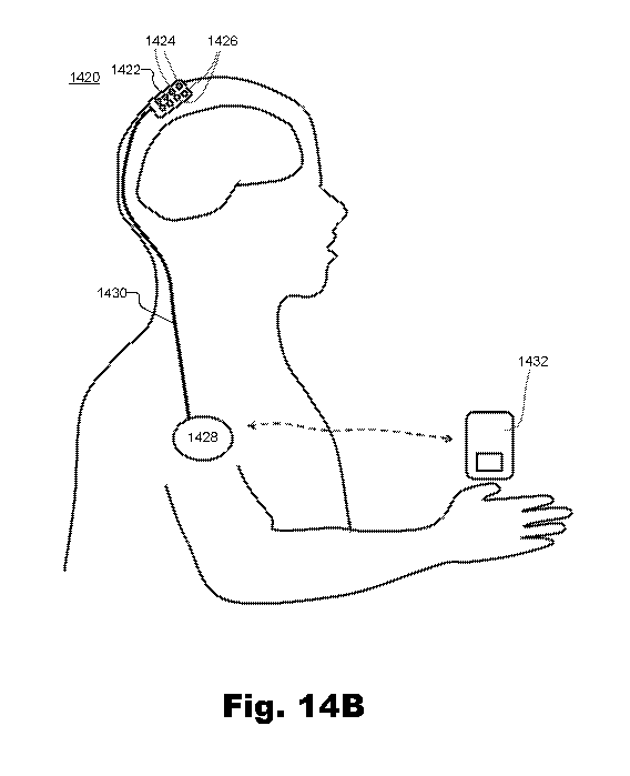
that is pre-
charged with a bias voltage before a command is provided to arm the SPAD. This
is
described more fully in U.S. Patent No. 10,158,038, incorporated above by
reference in
its entirety.
[0078] FIG. 15 illustrates an exemplary method 1500 for performing TCSPC
using a
photodetector system (e.g., any of the photodetector systems described
herein). While
FIG. 15 illustrates exemplary operations according to one embodiment, other
embodiments may omit, add to, reorder, and/or modify any of the operations
shown in
FIG. 15.
[0079] In operation 1502, a processor receives an accumulated output from a
plurality of photodetectors, the accumulated output representing an
accumulation of
respective outputs from each of the plurality of photodetectors detecting
photons during
a predetermined measurement time period that occurs in response to a light
pulse
being directed toward a target within a body. Operation 1502 may be performed
in any
.. of the ways described herein.
[0080] In operation 1504, the processor determines, based on the
accumulated
output, a temporal distribution of photons detected by the plurality of
photodetectors.
Operation 1504 may be performed in any of the ways described herein.
18
CA 03135228 2021-09-27
WO 2020/226840
PCT/US2020/027537
[0081] In operation 1506, the processor generates, based on the
temporal
distribution of photons, a histogram representing a light pulse response of
the target
within the body. Operation 1506 may be performed in any of the ways described
herein.
[0082] FIG. 16 illustrates an exemplary computing device 1600 that may
be
specifically configured to perform one or more of the processes described
herein. As
shown in FIG. 16, computing device 1600 may include a communication interface
1602,
a processor 1604, a storage device 1606, and an input/output (I/O") module
1608
communicatively connected one to another via a communication infrastructure
1610.
While an exemplary computing device 1600 is shown in FIG. 16, the components
illustrated in FIG. 16 are not intended to be limiting. Additional or
alternative
components may be used in other embodiments. Components of computing device
1600 shown in FIG. 16 will now be described in additional detail.
[0083] Communication interface 1602 may be configured to communicate
with one
or more computing devices. Examples of communication interface 1602 include,
without limitation, a wired network interface (such as a network interface
card), a
wireless network interface (such as a wireless network interface card), a
modem, an
audio/video connection, and any other suitable interface.
[0084] Processor 1604 generally represents any type or form of
processing unit
capable of processing data and/or interpreting; executing, and/or directing
execution of
one or more of the instructions, processes, and/or operations described
herein.
Processor 1604 may perform operations by executing computer-executable
instructions
1612 (e.g., an application, software, code, and/or other executable data
instance)
stored in storage device 1606.
[0085] Storage device 1606 may include one or more data storage media,
devices,
or configurations and may employ any type, form, and combination of data
storage
media and/or device. For example; storage device 1606 may include, but is not
limited
to, any combination of the non-volatile media and/or volatile media described
herein.
Electronic data, including data described herein, may be temporarily and/or
permanently stored in storage device 1606. For example, data representative of
computer-executable instructions 1612 configured to direct processor 1604 to
perform
any of the operations described herein may be stored within storage device
1606. In
some examples, data may be arranged in one or more databases residing within
storage device 1606.
19
CA 03135228 2021-09-27
WO 2020/226840
PCT/US2020/027537
[0086] I/O module 1608 may include one or more I/O modules configured
to receive
user input and provide user output. I/O module 1608 may include any hardware,
firmware, software, or combination thereof supportive of input and output
capabilities.
For example, I/O module 1608 may include hardware and/or software for
capturing user
input, including, but not limited to, a keyboard or keypad, a touchscreen
component
(e.g., touchscreen display), a receiver (e.g., an RF or infrared receiver),
motion
sensors, and/or one or more input buttons.
[0087] I/O module 1608 may include one or more devices for presenting
output to a
user, including, but not limited to, a graphics engine, a display (e.g., a
display screen),
one or more output drivers (e.g., display drivers), one or more audio
speakers, and one
or more audio drivers. In certain embodiments, I/O module 1608 is configured
to
provide graphical data to a display for presentation to a user. The graphical
data may
be representative of one or more graphical user interfaces and/or any other
graphical
content as may serve a particular implementation.
[0088] In some examples, any of the systems, computing devices, processors,
controller units, and/or other components described herein may be implemented
by
computing device 1600. For example, processor 108 and/or controller unit 112
may be
implemented by processor 1604.
[0089] In the preceding description, various exemplary embodiments have
been
described with reference to the accompanying drawings. It will, however, be
evident
that various modifications and changes may be made thereto, and additional
embodiments may be implemented, without departing from the scope of the
invention
as set forth in the claims that follow. For example, certain features of one
embodiment
described herein may be combined with or substituted for features of another
embodiment described herein. The description and drawings are accordingly to
be
regarded in an illustrative rather than a restrictive sense.