Note : Les descriptions sont présentées dans la langue officielle dans laquelle elles ont été soumises.
CONTROL SIGNAL MODULATION CIRCUIT, INVERTER, AND CONTROL
SYSTEM
FIELD
[0001] The present disclosure relates to the field of control technology, and
in particular to a
circuit for modulating a control signal, an inverter and a control system.
BACKGROUND
[0002] In a control system, a controller is required to perform signal
interaction with a
controlled object, to control the controlled object. For example, in a
photovoltaic system, an
inverter controls an operation state of a photovoltaic string, which requires
signal interaction
between the inverter and the photovoltaic string.
[0003] However, in the conventional technology, the signal interaction between
the
controller and the controlled object requires a dedicated communication
system, or has high
requirements for hardware. Therefore, a solution for modulating a control
signal which
requires no dedicated communication system and has low hardware cost is
urgently required.
SUMMARY
[0004] In view of the above, a circuit for modulating a circuit, an inverter
and a control
system are provided according to the present disclosure, so as to reduce
hardware cost without
a dedicated communication system. The technical solutions are described as
follows.
[0005] According to a first aspect of the present disclosure, a circuit for
modulating a
control signal is provided. The circuit includes a DC/DC boost circuit and a
control unit. The
DC/DC boost circuit includes a first capacitor, a first inductor, a first
controllable switch, a
- -
Date regue/date received 2022-10-11
CA 03136856 2021-10-13
second capacitor, and a controllable switch circuit. The first capacitor is
connected in parallel
with an input end of the DC/DC boost circuit. The second capacitor is
connected in parallel
with an output end of the DC/DC boost circuit. A terminal of the first
inductor is connected to
a positive input port of the DC/DC boost circuit, and another terminal of the
first inductor is
connected to a positive output port of the DC/DC boost circuit via the
controllable switch
circuit. A terminal of the first controllable switch is connected to a common
terminal of the
first inductor and the controllable switch circuit, and another terminal of
the first controllable
switch is connected to a negative input port. The control unit is configured
to control, when a
voltage of the first capacitor is greater than or equal to a first voltage
threshold, at least one of
a duty cycle of a signal for controlling the first controllable switch and a
frequency for
controlling the first controllable switch, to control the first capacitor to
generate a control
signal with a predetermined characteristic waveform.
[0006] In an embodiment, the controllable switch circuit includes a first
unidirectional
conduction device and a second controllable switch. An anode of the first
unidirectional
conduction device is connected to the first inductor, and a cathode of the
first unidirectional
conduction device is connected to a negative output port of the DC/DC boost
circuit. The
second controllable switch is connected in parallel with the first
unidirectional conduction
device. Alternatively, the second controllable switch is connected in parallel
with a branch
formed by connecting the first inductor in series with the first
unidirectional conduction
device.
[0007] In an embodiment, the controllable switch circuit further includes a
current limiting
device connected in series with the second controllable switch.
[0008] In an embodiment, the controllable circuit includes a third
controllable switch
connected in series with the first inductor.
[0009] In an embodiment, the control unit is further configured to: control
the controllable
switch circuit to be switched on when the voltage of the first capacitor is
greater than or equal
to the first voltage threshold, to charge the first capacitor by the second
capacitor; or control
the controllable switch circuit to be switched on when the first controllable
switch is
controlled to be switched off, to charge the first capacitor by the second
capacitor.
[0010] In an embodiment, the control unit is further configured to: control
the controllable
17609558.2
- 2 -
Date Recu/Date Received 2021-10-13
CA 03136856 2021-10-13
switch circuit to be switched on when a voltage of the second capacitor is
greater than or
equal to a second voltage threshold, to control the second capacitor to
discharge.
100111 In an embodiment, the circuit further includes a direct current power
supply circuit, a
fourth controllable switch and a second unidirectional conduction device. An
output port of
.. the direct current power supply circuit is connected in series with the
fourth controllable
switch and the second unidirectional conduction device sequentially, and is
connected to the
input end of the DC/DC boost circuit. An alternating current end of the direct
current power
supply circuit is configured to connect with an alternating current power
supply. The second
unidirectional conduction device is configured to cause electric energy
outputted by the direct
.. current power supply circuit to flow to the input end of the DC/DC boost
circuit. The control
unit is further configured to: control the fourth controllable switch to be
switched on when the
voltage of the first capacitor is less than or equal to the first voltage
threshold, to charge the
first capacitor by the direct current power supply circuit; or control the
fourth controllable
switch to be switched on when the first controllable switch is controlled to
be switched off, to
charge the first capacitor by the direct current power supply circuit.
[0012] According to a second aspect of the present disclosure, an inverter is
provided. The
inverter includes an inverter circuit, an inverter controller and the circuit
for modulating a
control signal described in the first aspect. The output end of the DC/DC
boost circuit is
connected to a direct current end of the inverter circuit, and the input end
of the DC/DC boost
circuit is configured to connect a photovoltaic string. The inverter
controller is configured to:
acquire a control signal generation instruction; and transmit the control
signal generation
instruction to the control unit of the circuit for modulating a control
signal, where the control
unit controls the first capacitor to generate the control signal with the
predetermined
characteristic waveform.
[0013] In an embodiment, the inverter controller is configured to transmit, in
response to an
instruction for switching off the photovoltaic string, a switch-off signal
generation instruction
to the control unit, where the control unit controls a switch state of the
first controllable
switch in the DC/DC boost circuit in response to the switch-off signal
generation instruction,
to control the first capacitor to generate a switch-off control signal with a
first characteristic
waveform. The inverter controller is further configured to transmit, in
response to an
17609558.2
- 3 -
Date Recu/Date Received 2021-10-13
CA 03136856 2021-10-13
instruction for switching on the photovoltaic string, a switch-on signal
generation instruction
to the control unit, where the control unit controls, in response to the
switch-on signal
generation instruction, the second capacitor of the DC/DC boost circuit or the
direct current
power supply circuit to charge the first capacitor until the voltage of the
first capacitor reaches
the first voltage threshold, where a switch state of the first controllable
switch is controlled, to
control the first capacitor to generate a switch-on control signal with a
second characteristic
waveform.
[0014] In an embodiment, the inverter includes multiple direct current input
ends
respectively connected to circuits for modulating a control signal as
described in the first
aspect. For each of the circuits for modulating a control signal, the input
end of the DC/DC
boost circuit is connected to a direct current input end of the inverter
corresponding to the
circuit for modulating a control signal. Output ends of all the DC/DC boost
circuits are
connected in parallel and are connected to a direct current input end of the
inverter circuit. All
the DC/DC boost circuits share the second controllable switch, or share the
fourth controllable
switch, the second unidirectional conduction device and the direct current
power supply
circuit.
[0015] According to a third aspect of the present disclosure, a system for
controlling a
photovoltaic string is further provided. The system includes the inverter
described in the
second aspect and at least one photovoltaic string. Each of the at least one
photovoltaic string
includes multiple photovoltaic modules connected in series and multiple
circuit breakers
connected to output ends of the multiple photovoltaic modules in one to one
correspondence.
All of the multiple circuit breakers are connected in series and are connected
to a direct
current input end of the inverter. Each of the multiple circuit breakers is
configured to analyze
a control signal outputted by the inverter to obtain a control instruction,
and respond to the
control instruction.
[0016] In an embodiment, for analyzing the control signal outputted by the
inverter to
obtain the control instruction and respond to the control instruction, the
circuit breaker is
configured to: determine, when determining that the control signal outputted
by the inverter
has a first predetermined characteristic waveform, that the control signal is
a switch-off
control signal, to switch off a photovoltaic module connected to the circuit
breaker; and
17609558.2
- 4 -
Date Recu/Date Received 2021-10-13
CA 03136856 2021-10-13
determine, when determining that the control signal outputted by the inverter
has a second
predeteimined characteristic waveform, that the control signal is a switch-on
control signal, to
switch on the photovoltaic module connected to the circuit breaker,
[0017] In an embodiment, each of the multiple photovoltaic modules in the
photovoltaic
string is provided with a component controller. The component controller is
configured to
determine, when it is determined that the control signal outputted by the
inverter has a third
predetermined characteristic waveform, that the control signal is a monitoring
signal, to
upload state data of the photovoltaic module to the inverter.
[0018] A circuit for modulating a control signal, an inverter and a control
system are
provided according to the present disclosure. The circuit for modulating a
control signal is
based on a DC/DC boost circuit. The DC/DC boost circuit includes a
controllable switch
circuit, via which a second capacitor charges a first capacitor. A switch
state of the first
controllable switch is controlled when a voltage of the first capacitor is
greater than or equal
to a first voltage threshold, so that the first capacitor generates a control
signal with a
predetermined characteristic waveform. With this solution, the control signal
with the
predetermined characteristic waveform is generated by the first capacitor in
the DC/DC boost
circuit being charged and discharging, without a dedicated signal generator or
a power line
communication module (PLC), leading to low hardware cost. Moreover, compared
with
wireless communication, the control signal generated with this solution is not
affected by a
distance and therefore crosstalk cannot occur, so that there is no special
requirement for
topography of an installation site.
BRIEF DESCRIPTION OF THE DRAWINGS
[0019] In order to more clearly describe the technical solutions in the
embodiments of the
present disclosure or the technical solutions in the conventional technology,
drawings to be
used in the description of the embodiments of the present disclosure or the
conventional
technology are briefly described hereinafter. It is apparent that the drawings
described below
show merely the embodiments of the present disclosure, and those skilled in
the art may
obtain other drawings according to the provided drawings without any creative
effort.
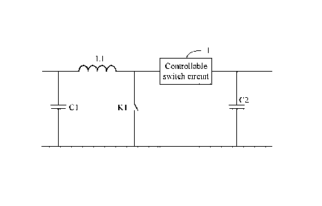
[0020] Figure 1 is a schematic diagram showing circuit for modulating a
control signal
17609558.2
- 5 -
Date Recu/Date Received 2021-10-13
CA 03136856 2021-10-13
according to an embodiment of the present disclosure;
[0021] Figure 2 is a schematic diagram showing a circuit for modulating a
control signal
according to another embodiment of the present disclosure;
[0022] Figure 3 is a schematic diagram showing six characteristic waveforms
according to
an embodiment of the present disclosure;
[0023] Figure 4 is a schematic diagram showing a circuit for modulating a
control signal
according to another embodiment of the present disclosure;
[0024] Figure 5 is a schematic diagram showing a circuit for modulating a
control signal
according to another embodiment of the present disclosure;
[0025] Figure 6 is a schematic diagram of showing a circuit for modulating a
control signal
according to another embodiment of the present disclosure;
[0026] Figure 7 is a structural schematic diagram showing an inverter
according to an
embodiment of the present disclosure;
[0027] Figure 8 is a structural schematic diagram showing an inverter
according to another
embodiment of the present disclosure;
[0028] Figure 9 is a structural schematic diagram showing an inverter
according to another
embodiment of the present disclosure;
[0029] Figure 10 is a structural schematic diagram showing an inverter
according to another
embodiment of the present disclosure;
[0030] Figure 11 is a structural schematic diagram showing an inverter
according to another
embodiment of the present disclosure;
[0031] Figure 12 is a structural schematic diagram showing a system for
controlling a
photovoltaic string according to an embodiment of the present disclosure; and
[0032] Figure 13 is a structural schematic diagram showing an internal
structure of a circuit
breaker according to an embodiment of the present disclosure.
DETAILED DESCRIPTION OF EMBODIMENTS
17609558.2
- 6 -
Date Recu/Date Received 2021-10-13
CA 03136856 2021-10-13
[0033] In order to make the purpose, technical solutions and advantages of
embodiments of
the present disclosure clearer, the technical solutions of embodiments of the
present disclosure
are described below clearly and completely in conjunction with the drawings of
the
embodiments of the present disclosure. Apparently, the embodiments described
below are
only some rather than all of the embodiments of the present disclosure. Any
other
embodiments obtained by those skilled in the art based on the embodiments in
the present
disclosure without any creative effort fall within the protection scope of the
present
disclosure.
[0034] Reference is made to Figure 1, which is a structural schematic diagram
showing a
circuit for modulating a control signal according to an embodiment of the
present disclosure.
The circuit is based on a DC/DC boost circuit. As shown in Figure 1, the
circuit includes a
DC/DC boost circuit and a control unit.
[0035] The DC/DC boost circuit includes a first capacitor Cl, a first inductor
Li, a first
controllable switch Kl, a second capacitor C2, and a controllable switch
circuit 1 connected in
series in a circuit for charging the capacitor Cl.
[0036] The first capacitor Cl is connected in parallel to an input end of the
DC/DC boost
circuit. The second capacitor C2 is connected in parallel with an output end
of the DC/DC
boost circuit. One terminal of the inductor Li is connected to a positive
input port of the
DC/DC boost circuit, and the other terminal of the inductor Li is connected to
a positive
output port of the DC/DC boost circuit via the controllable switch circuit 1.
[0037] One terminal of the first controllable switch K1 is connected to a
common terminal
of the inductor Li and the controllable switch circuit 1, and the other
telininal of the first
controllable switch K1 is connected to a negative input port of the DC/DC
boost circuit.
[0038] The control unit is configured to control a switch state of the first
controllable switch
when a voltage of the first capacitor Cl is greater than or equal to a first
voltage threshold,
so that the first capacitor Cl generates a control signal with a predetermined
characteristic
waveform. When the first controllable switch K1 is switched on, the first
capacitor C 1
discharges. When the first controllable switch K1 is switched off, the first
capacitor CI stops
discharging. The predetermined characteristic waveform is generated by the
first capacitor Cl
by controlling at least one of a duty cycle of a signal for controlling the
first controllable
17609558.2
- 7 -
Date Recu/Date Received 2021-10-13
CA 03136856 2021-10-13
switch and a frequency for controlling the first controllable switch K1 to be
switched on or
off.
[0039] In an application scenario, the voltage of the first capacitor Cl
decreases as the first
capacitor Cl discharges. When the voltage of the first capacitor C 1 is less
than a threshold, the
first capacitor Cl cannot generate the control signal with the predetermined
characteristic
waveform. In this case, it is required to charge the first capacitor Cl to
increase the voltage of
the first capacitor Cl. In this embodiment, a branch, in the controllable
switch circuit 1, for
the second capacitor C2 to charge the first capacitor Cl is controlled to be
switched on, so that
the second capacitor C2 charges the first capacitor C 1. When charging the
first capacitor Cl, a
voltage of the second capacitor C2 decreases, so that the voltage of the
second capacitor C2 is
released, thereby reducing a risk of overvoltage of the second capacitor C2.
[0040] In an embodiment, the voltage of the first capacitor Cl is detected.
The branch, in
the controllable switch circuit 1, for the second capacitor C2 to charge the
first capacitor Cl is
controlled to be switched on when the voltage on the first capacitor C 1 is
less than the first
voltage threshold, so that the second capacitor C2 charges the first capacitor
Cl.
[0041] In another embodiment, every time the first controllable switch K1 is
controlled to
be switched off, the branch, in the controllable switch circuit 1, for the
second capacitor C2 to
charge the first capacitor Cl is controlled to be switched on, so that the
first capacitor Cl
discharges and is charged alternately, thereby preventing the voltage of the
first capacitor Cl
___________________________________________ from being too low to generate the
preset characteristic wavefoi in.
[0042] The circuit for modulating a control signal according to the embodiment
is based on
a DC/DC boost circuit. The DC/DC boost circuit includes a controllable switch
circuit, via
which the second capacitor charges the first capacitor. The switch state of
the first controllable
switch is controlled when the voltage of the first capacitor is greater than
or equal to the first
voltage threshold, so that the first capacitor generates the control signal
with the
predetermined characteristic waveform. With this solution, the control signal
with the
predetermined characteristic waveform is generated by the first capacitor in
the DC/DC boost
circuit being charged and discharging. Therefore, neither a dedicated signal
generator nor a
PLC communication module is required, leading to low hardware cost. Moreover,
compared
with wireless communication, the control signal generated with this solution
is not affected by
17609558.2
- 8 -
Date Recu/Date Received 2021-10-13
CA 03136856 2021-10-13
a distance and therefore crosstalk cannot occur, so that there is no special
requirement for
topography of an installation site.
[0043] Reference is made to Figure 2, which is a schematic diagram showing a
circuit for
modulating a control signal according to another embodiment of the present
disclosure. The
circuit is based on a typical boost circuit.
[0044] As shown in Figure 2, the typical boost circuit includes a first
capacitor Cl, a first
inductor Li, a first controllable switch 1(1, a first unidirectional
conduction device D1 and a
second capacitor C2. The first capacitor Cl is connected in parallel with an
input end of the
boost circuit, and the second capacitor C2 is connected in parallel with an
output end of the
boost circuit. The first inductor Li and the first unidirectional conduction
device D1 are
connected in series between a positive input port and a positive output port
of the boost circuit.
One terminal of the first controllable switch KI is connected to a common
terminal of the first
inductor Li and the first unidirectional conduction device D1, and the other
terminal of the
first controllable switch K1 is connected to a negative input port of the
boost circuit. A second
controllable switch K2 is connected in parallel with the first unidirectional
conduction device
Dl,
[0045] The boost circuit is also known as a boost step up circuit, which is a
switch direct
current boost circuit and is capable of increasing an input voltage.
[0046] The second controllable switch 1(2 is added to the typical boost
circuit. In an
embodiment, the second controllable switch 1(2 is connected in parallel with
the first
unidirectional conduction device Dl. That is, the second controllable switch
K2 and the first
unidirectional conduction device DI form the controllable switch circuit 1 in
the embodiment
shown in Figure 1.
[0047] The second controllable switch K2 is configured to provide a branch for
the second
capacitor C2 to charge the first capacitor Cl. The second controllable switch
K2 is controlled
to be switched on when the voltage of the first capacitor C 1 is less than the
first voltage
threshold. In this case, energy of the second capacitor C2 flows to the first
capacitor Cl via
the second controllable switch K2 and the first inductor Li, that is, the
second capacitor C2
charges the first capacitor Cl. When the voltage of the first capacitor Cl
reaches the first
voltage threshold, the first capacitor Cl is controlled to be charged or to
discharge by
17609558.2
- 9 -
Date Recu/Date Received 2021-10-13
CA 03136856 2021-10-13
controlling the switch state of the first controllable switch K1 to be
switched on or switched
off, so that first capacitor Cl generates a voltage signal with the
predetermined characteristic
waveform.
[0048] The first voltage threshold is determined based on a parameter of the
first capacitor
Cl. When the voltage of the first capacitor Cl reaches the first voltage
threshold and a control
signal is required, the first controllable switch K1 is controlled to be
switched on, so that the
first capacitor Cl discharges and the voltage of the first capacitor Cl
decreases. The switch
state of the first controllable switch K1 is controlled based on a preset duty
cycle of a signal
and a preset frequency, so that the first capacitor Cl generates a control
signal with a preset
characteristic waveform.
[0049] In the photovoltaic field, a direct current power supply connected to
the input end of
the boost circuit is usually a photovoltaic string. In a case that the
photovoltaic string is
switched on, the first capacitor Cl is charged by the photovoltaic string, so
that the voltage of
the first capacitor Cl increases. Alternatively, the second controllable
switch K2 is controlled
to be switched on, so that the first capacitor Cl is charged by the second
capacitor C2. The
second capacitor C2 charges the first capacitor Cl as long as the voltage of
the second
capacitor C2 is greater than the voltage of the first capacitor Cl, regardless
of whether the
photovoltaic string on the direct current side is switched on.
[0050] It should be noted that the second controllable switch K2 is controlled
to be switched
on when the voltage of the first capacitor Cl is less than the first voltage
threshold, so that the
first capacitor Cl is charged by the second capacitor C2. Alternatively, every
time the first
controllable switch Kl is controlled to be switched off, the second
controllable switch K2 is
controlled to be switched on, so that the first capacitor CI is charged by the
second capacitor
C2.
[0051] In another application scenario of the present disclosure, when
controlling the switch
state of the first controllable switch Kl, the voltage of the second capacitor
C2 may exceed a
safety threshold. In this case, the second controllable switch K2 is
controlled to be switched
on, to release the voltage of the second capacitor C2, so as to reduce the
risk of overvoltage of
the second capacitor C2.
[0052] Figure 3 shows six characteristic waveforms according to an embodiment
of the
17609558.2
- 10 -
Date Recu/Date Received 2021-10-13
CA 03136856 2021-10-13
present disclosure. Apparently, other characteristic waveforms can be obtained
and are not
shown in the present disclosure.
[0053] The characteristic waveform varies with the control signal. The
corresponding
relationship between a control signal and its characteristic waveform is pre-
determined and
stored in the control unit. When a control signal is required, a
characteristic waveform
corresponding to the control signal is obtained based on the corresponding
relationship, and
then the control signal having the characteristic waveform is generated.
[0054] In another embodiment of the present disclosure, as shown in Figure 4,
the second
controllable switch 1(2 is connected in parallel with a branch formed by
connecting the first
inductor Li in series with the first unidirectional conducting device Di. The
circuit shown in
Figure 4 operates in the same way as the circuit shown in Figure 1, and is not
repeated herein.
[0055] In addition, an inrush current is generated at a time instant at which
the second
controllable switch 1(2 is switched on, which reduces a service life of the
switch. In another
embodiment of the present disclosure, as shown in Figure 4, a current limiting
device such as
a resistor or an inductor is connected in series with the second controllable
switch K2 so as to
reduce the inrush current generated at the time instant at which the second
controllable switch
1(2 is switched on. Apparently, the circuit according to the embodiment shown
in Figure 2
may further include a current limiting device connected in series with the
second controllable
switch K2, which is not described in detail herein.
[0056] In another embodiment of the present disclosure, as shown in Figure 5,
the
controllable switch circuit is implemented by a third controllable switch 1(3.
The first
controllable switch 1(1 and the third controllable switch K3 in this
embodiment respectively
operate in the same way as the first controllable switch K1 and the second
controllable switch
1(2 in Figures 2 and 4, and are not be described in detail here.
[0057] The circuit for modulating a control signal according to the embodiment
is based on
the typical boost circuit. A second controllable switch is added to the
typical boost circuit. The
second controllable switch is controlled to be switched on when the voltage on
the first
capacitor is less than the first voltage threshold, so that the first
capacitor is charged by the
second capacitor until the voltage on the first capacitor reaches the first
voltage threshold. The
switch state of the first controllable switch is controlled, so that the first
capacitor generates
17609558.2
- 11 -
Date Recu/Date Received 2021-10-13
CA 03136856 2021-10-13
the control signal with the predetermined characteristic waveform. With this
solution, the
control signal with the predetermined characteristic waveform is generated by
the first
capacitor in the boost circuit being charged and discharging. Therefore,
neither a signal
generator nor a PLC communication module is required, leading to low hardware
cost.
Moreover, compared with the wireless communication, the control signal
generated with this
solution is not affected by a distance and therefore crosstalk cannot occur,
so that there is no
special requirement for topography of an installation site.
[0058] In the above embodiments, the second capacitor C2 charges the first
capacitor Cl in
the DC/DC boost circuit, so that the voltage on the first capacitor Cl reaches
a voltage
required for generating the predetermined characteristic waveform. In another
embodiment of
the present disclosure, the first capacitor Cl is charged by a direct current
power supply
circuit.
[0059] Reference is made to Figure 6, which is a schematic diagram showing a
circuit for
modulating a control signal according to another embodiment of the present
disclosure. The
circuit according to this embodiment is based on the DC/DC boost circuit.
Different from the
embodiments shown in Figures 2, 4 and 5, the first capacitor Cl in this
embodiment is
charged by a direct current power supply circuit.
[0060] As shown in Figure 6, the circuit for modulating a control signal
includes a direct
current power supply circuit 110, a second unidirectional conduction device
D2, a fourth
controllable switch K4, a DC/DC boost circuit 120 and a control unit.
[0061] The DC/DC boost circuit 120 in this embodiment adopts any one of DC/DC
boost
topologies shown in Figures 2, 4 and 5, and these boost topologies are not
repeated herein. A
case in which the DC/DC boost circuit 120 is implemented by the circuit shown
in Figure 2 is
taken as an example for description in this embodiment.
[0062] An output port of the direct current power supply circuit 110 is
connected in series
with the fourth controllable switch K4 and the second unidirectional
conduction device D2
sequentially, and is connected to an input port of the DC/DC boost circuit
120.
[0063] In this embodiment, the second unidirectional conduction device D2 is
configured to
cause electric energy outputted by the direct current power supply circuit to
flow to the input
17609558.2
- 12 -
Date Recu/Date Received 2021-10-13
CA 03136856 2021-10-13
end of the DC/DC boost circuit, thereby preventing energy from flowing from
the DC/DC
boost circuit to the direct current power supply circuit.
[0064] In an embodiment of the present disclosure, the direct current power
supply circuit
110 is implemented by an inverter circuit, and an alternating current side of
the inverter circuit
is connected to an alternating current power supply.
[0065] When the voltage of the first capacitor Cl is greater than or equal to
the first voltage
threshold, at least one of a duty cycle of a signal for controlling first
controllable switch K1
and a frequency for controlling the first controllable switch K1 is
controlled, so that the first
capacitor generates a control signal with a predetermined characteristic
waveform.
[0066] In an embodiment of the present disclosure, when the voltage of the
first capacitor
Cl is less than the first voltage threshold, the fourth controllable switch K4
is controlled to be
switched on, so that the first capacitor Cl is charged by the direct current
power supply circuit
110.
[0067] In another embodiment of the present disclosure, the fourth
controllable switch K4 is
controlled to be switched on when the first controllable switch K1 is
controlled to be switched
off, so that the direct current power supply circuit charges the first
capacitor Cl.
[0068] In another embodiment of the present disclosure, in order to prevent
the voltage of
the second capacitor C2 from exceeding the safety threshold, the second
controllable switch
K2 is controlled to be switched on when it is detected that the voltage of the
second capacitor
C2 is greater than a second voltage threshold, so that the second capacitor C2
discharges, so
as to reduce the risk of overvoltage of the second capacitor C2.
[0069] Alternatively, in other embodiments, a direct current load (such as a
fan) in the
circuit is controlled to operate when the voltage on the second capacitor C2
exceeds the
second voltage threshold, to consume the energy of the second capacitor C2, so
as to reduce
the risk of overvoltage of the second capacitor C2.
[0070] In an embodiment of the present disclosure, in an application scenario
where the
circuit for modulating a control signal is applied to an inverter, the direct
current power supply
circuit 110 is implemented by a power supply circuit in the inverter. For
example, the direct
current power supply circuit 110 is implemented by a power supply circuit
configured to
17609558.2
- 13 -
Date Recu/Date Received 2021-10-13
CA 03136856 2021-10-13
supply power to a direct current load (such as a fan) of the inverter. A
supply voltage of the
power supply circuit is +24V or the like. Alternatively, in other embodiments,
the direct
current power supply circuit 110 is implemented by a direct current power
supply circuit
rather than a direct current power supply in the inverter, which is not
described in detail
herein.
[0071] In the circuit for modulating a control signal according to this
embodiment, the first
capacitor Cl is charged by a direct current power supply circuit. When the
voltage of the first
capacitor is less than the first voltage threshold, the fourth controllable
switch circuit is
controlled to be switched on, so that the first capacitor is charged by the
direct current power
supply circuit. When the voltage of the first capacitor reaches the first
voltage threshold, the
switch state of the first controllable switch is controlled, so that the first
capacitor discharges
or is charged, to generate the control signal with the predetermined
characteristic waveform
on. With this solution, the direct current power supply circuit charges the
first capacitor
without affecting the second capacitor C2, thereby improving reliability of
the DC/DC boost
circuit.
[0072] According to another aspect of the embodiments of the present
disclosure, an
inverter to which the above circuit for modulating a control signal is applied
is provided.
[0073] Reference is made to Figure 7, which is a structural schematic diagram
showing an
inverter according to an embodiment of the present disclosure. A single-input
inverter is taken
as an example for description in this embodiment.
[0074] As shown in Figure 7, the inverter includes a circuit 210 for
modulating a control
signal, an inverter circuit 220 and an inverter controller.
[0075] The circuit 210 for modulating a control signal is implemented by
adding a second
controllable switch K2 to a boost circuit of the inverter. That is, the
circuit 210 for modulating
a control signal is implemented by the circuit shown in Figure 2. The boost
circuit includes a
first capacitor C 1 , a first inductor Li, a first controllable switch Kl, a
first unidirectional
conduction device D1, and a second capacitor C2.
[0076] In this embodiment, the second controllable switch 1(2 is connected in
parallel with
the first unidirectional conduction device D1 in the boost circuit. An output
end of the boost
17609558.2
- 14 -
Date Recu/Date Received 2021-10-13
CA 03136856 2021-10-13
circuit is connected to a direct current end of the inverter circuit 220. An
input end of the
boost circuit is configured to connect a photovoltaic string.
[0077] The inverter controller is configured to acquire a control signal
generation
instruction and transmit the control signal generation instruction to the
control unit in the
circuit for modulating a control signal.
[0078] The control unit is configured to control the second controllable
switch K2 to be
switched off when a voltage of the first capacitor Cl is greater than or equal
to a first voltage
threshold, and control a switch state of the first controllable switch K1 so
that the first
capacitor Cl generates a control signal with a predeteimined characteristic
waveform.
[0079] The control signal is analyzed by a control module in the photovoltaic
string to
obtain a control instruction, and the control instruction is executed by the
control module.
[0080] The control unit is further configured to control the second
controllable switch K2 to
be switched on when the voltage of the first capacitor Cl is less than the
first voltage
threshold, so that the second capacitor C2 charges the first capacitor Cl.
[0081] In addition, the control unit is integrated in the inverter controller.
Alternatively, the
control unit is separated from the inverter controller.
[0082] In an application scenario, the inverter is required to generate a
control signal for
controlling the photovoltaic module to be switched on or switched off In this
application
scenario, the control unit operates as follows.
[0083] In a case that the photovoltaic string is switched on, the voltage
across the first
capacitor Cl is equal to a voltage Ul across the photovoltaic string, and the
voltage Ul is
greater than zero. In this case, when the inverter controller acquires a
switch-off instruction
(for example, generated when it is detected that an external DI interface
receives a trigger
signal generated by a button), the inverter is shut down. In addition, the
inverter controller
generates a switch-off signal generation instruction and transmits the switch-
off signal
generation instruction to the control unit in the circuit for modulating a
control signal. When
receiving the switch-off signal generation instruction, the control unit
controls the second
controllable switch K2 to be switched off and controls the first controllable
switch K1 to be
switched on. Since the first capacitor Cl is connected in parallel between
positive and
17609558.2
- 15 -
Date Recu/Date Received 2021-10-13
CA 03136856 2021-10-13
negative ports of the photovoltaic string, and the first inductor Li is
connected in parallel with
the first capacitor Cl, the first capacitor Cl discharges via the first
inductor Li and therefore
the voltage of the first capacitor Cl decreases. When the first controllable
switch K1 is
switched off, the photovoltaic string charges the first capacitor Cl and
therefore the voltage of
.. the first capacitor CI increases. Alternatively, the control unit controls
the second controllable
switch K2 to be switched on, so that the second capacitor C2 charges the first
capacitor Cl,
and therefore the voltage of the first capacitor Cl increases. By controlling
the switch state of
the first controllable switch K1 based on a predetermined duty cycle and at a
predetermined
frequency, the first capacitor C 1 generates a switch-off control signal with
a first
predetermined characteristic waveform.
[0084] In a case that the photovoltaic string is switched off, the voltage of
the first capacitor
Cl approximates zero. When receiving a switch-on instruction, the inverter
controller
generates a switch-on signal generation instruction and transmits the switch-
on signal
generation instruction to the control unit. Since the photovoltaic string is
switched off, the first
capacitor Cl cannot be charged by the photovoltaic string. Therefore, when the
control unit
receives the switch-on signal instruction, a direct current bus is pre-charged
by a grid on the
alternating current side to increase a voltage of the direct current bus.
Then, the first
controllable switch K1 is controlled to be switched off and the second
controllable switch K2
is controlled to be switched on. In this case, the second capacitor C2 charges
the first
.. capacitor Cl. When the voltage on the first capacitor Cl reaches the first
voltage threshold,
the switch state of the first controllable switch K1 is controlled, so that
the first controllable
switch Cl generates a switch-on control signal with a second predetermined
characteristic
waveform.
[0085] The switch-off control signal may have any one of the characteristic
waveforms
shown in Figure 3. Alternatively, the switch-off control signal has another
characteristic
waveform not shown in Figure 3. The switch-on control signal has a
characteristic waveform
different from the characteristic waveform of the switch-off control signal,
which is not
limited in the present disclosure.
[0086] In another embodiment of the present disclosure, in order to reduce an
inrush current
generated at a time instant when the second controllable switch K2 is switched
on, a current
17609558.2
- 16 -
Date Recu/Date Received 2021-10-13
CA 03136856 2021-10-13
limiting device such as a resistor or an inductor is connected in series with
the second
controllable switch K2.
[0087] In another embodiment of the present disclosure, as shown in Figure 8,
the second
controllable switch K2 (or a branch formed by connecting the second
controllable switch K2
in series with the current limiting device) is connected in parallel with the
a branch formed by
connecting the first inductor Li is series with the unidirectional conduction
device Dl.
Generation of the control signal in the embodiment shown in Figure 8 is the
same as the
generation of the control signal by the inverter shown in Figure 7, and is not
described in
detail herein.
[0088] In another application scenario of the present disclosure, the inverter
includes
multiple direct current input ends. A case in which the inverter includes two
direct current
input ends is taken as an example for description below.
[0089] As shown in Figure 9, an output end of a boost circuit is connected in
parallel with
an output end of another boost circuit. That is, a positive output port and a
negative output
port of a first boost circuit 310 are connected to a positive output port and
a negative output
port of a second boost circuit 320, respectively. Moreover, the two boost
circuits share a
controllable switch K2 (that is, the second controllable switch) and a current
limiting device.
[0090] One terminal of the controllable switch K2 is connected to the positive
output port of
the first boost circuit 310 and the positive output port of the second boost
circuit 320, and the
other terminal of the second controllable switch 1(2 is connected to a
positive input port of the
first boost circuit 310 via a second unidirectional conducting device D2, and
is further
connected with a positive input port of the second boost circuit 320 via a
second
unidirectional conducting device D21.
[0091] In another embodiment of the present disclosure, the second
controllable switch K2
is connected in parallel with a first unidirectional conduction device of each
boost circuit. As
shown in Figure 10, one terminal of the second controllable switch 1(2 is
connected to a
positive output port of each boost circuit, and the other terminal of the
second controllable
switch K2 is connected with a common terminal of a first inductor Li and a
first
unidirectional conducting device D1 in the first boost circuit 310 via the
second unidirectional
conducting device D2, and is further connected to a common terminal of a first
inductor L2
17609558.2
- 17 -
Date Recu/Date Received 2021-10-13
CA 03136856 2021-10-13
and a first unidirectional conducting device Dll in the second boost circuit
320 via the second
unidirectional conducting device D21.
[0092] The second unidirectional conducting devices D2 and D21 in Figures 9
and 10 are
unidirectionally conductive, so that energy only flows from the second
capacitor C2 to the
first capacitor Cl and flows from the second capacitor C21 to the first
capacitor C11, thereby
preventing electric energy in one boost circuit from flowing to another boost
circuit.
[0093] In the inverter circuits shown in Figures 9 and 10, the boost circuits
share the second
controllable switch K2 and the current limiting device, thereby further
reducing the hardware
cost.
[0094] In the inverter according to the embodiment, the first capacitor
connected in series
with the input end of the boost circuit generates a control signal a
predetermined characteristic
waveform by controlling the switch state of the controllable switch in the
boost circuit. When
the voltage of the first capacitor is less than the first voltage threshold,
the second controllable
switch is controlled to be switched on, so that the first capacitor is charged
by the second
capacitor, ensuring that the characteristic waveform generated by the first
capacitor is not
affected. With this solution, a control signal is generated by the improved
boost circuit and is
transmitted by an existing transmission line. With this solution, transmission
of the control
signal is not affected by a distance and therefore crosstalk does not occur,
so that there is no
special requirement for topography of an installation site. In addition,
neither a PLC
communication module nor a signal generator is required, leading to low
hardware cost.
[0095] An inverter to which the circuit for modulating a control signal shown
in Figure 6 is
applied is further provided according to an embodiment of the present
disclosure.
[0096] Reference is made to Figure 11, which is a structural schematic diagram
showing an
inverter according to another embodiment of the present disclosure. The
inverter includes a
circuit 410 for modulating a control signal, a boost circuit 420 and an
inverter circuit 430.
[0097] The circuit for modulating a control signal 410 includes a direct
current power
supply circuit 411, a controllable switch K, a third unidirectional conduction
device D and a
control unit.
[0098] A direct current output port of the direct current power supply circuit
411 is
17609558.2
- 18 -
Date Recu/Date Received 2021-10-13
CA 03136856 2021-10-13
connected in series with the controllable switch K and the third
unidirectional conduction
device D sequentially, and is connected to a direct current input port of the
boost circuit 420.
An alternating current end of the direct current power supply circuit 411 is
configured to
connect with an alternating current power supply.
[0099] A first controllable switch K1 in the DC/DC boost circuit 420 is
controlled by a
control unit, so that a first capacitor in the DC/DC boost circuit 420
generates a control signal
with a predetermined characteristic waveform.
[0100] When a voltage of the first capacitor Cl in the DC/DC boost circuit 420
is less than
a first voltage threshold or when the first controllable switch Kl in the
DC/DC boost circuit
420 is controlled to be switched off, the controllable switch K is controlled
to be switched on,
so that the first capacitor Cl is charged by the direct current power supply
circuit 411, so as to
increase the voltage of the first capacitor Cl.
101011 The control unit of the circuit for modulating a control signal in this
embodiment is
integrated in the inverter controller or separated from the inverter
controller.
[0102] In the inverter according to this embodiment, the direct current power
supply circuit
charges the first capacitor. When the voltage of the first capacitor is less
than the first voltage
threshold, a fourth controllable switch circuit is controlled to be switched
on, so that the first
capacitor is charged by the direct current power supply circuit. When the
voltage of the first
capacitor reaches the first voltage threshold, a switch state of the first
controllable switch is
controlled so that the first capacitor discharges or is charged, so as to
generate a control signal
with a predetermined characteristic waveform. With this solution, the direct
current power
supply circuit charges the first capacitor without affecting the second
capacitor, thereby
improving reliability of the inverter.
[0103] According to another aspect of the embodiments of the present
disclosure, a system
for controlling a photovoltaic string is further provided.
[0104] Reference is made to Figure 12, which is a structural schematic diagram
showing a
system for controlling a photovoltaic string according to an embodiment of the
present
disclosure. In the embodiment, the photovoltaic string is controlled by the
inverter shown in
Figure 7.
17609558.2
- 19 -
Date Recu/Date Received 2021-10-13
CA 03136856 2021-10-13
[0105] As shown in Figure 12, the system for controlling a photovoltaic string
includes an
inverter 610 and a photovoltaic string 620.
101061 The photovoltaic string 620 includes n photovoltaic modules PV1 to PVn
connected
in series, and n circuit breakers RSD1 to RSDn respectively connected to
output ends of the n
photovoltaic modules.
101071 The n photovoltaic modules are connected in series sequentially by
connecting the n
RSDs (Rapid Shutdowns) in series sequentially.
[0108] The n circuit breakers in the photovoltaic string 620 are connected in
series to the
direct current end of the inverter 610. Each of then circuit breakers is
configured to receive a
control signal outputted by the inverter, analyze the control signal to obtain
a control
instruction and respond to the control instruction.
[0109] Figure 13 is a structural schematic diagram showing an internal
structure of a circuit
breaker. The circuit breaker includes an analysis module 710, a controller
720, and a switch
transistor S.
[0110] In an application scenario where a photovoltaic module is controlled to
be switched
on or switched off, the circuit breaker operates as follows.
[0111] In a case that the analysis module 710 analyzes that the control signal
outputted by
the inverter has the first predetermined characteristic waveform, it is
determined that the
control signal is a switch-off control signal and the controller 720 controls
the switch
transistor S to be switched off, so as to disconnect a photovoltaic module
connected to the
switch transistor S from the inverter.
[0112] In a case that the analysis module 710 analyzes that the control signal
outputted by
the inverter has the second determined characteristic waveform, it is
determined that the
control signal is a switch-on control signal and the controller 720 controls
the switch transistor
S to be switched on, so as to connect a photovoltaic module connected to the
switch transistor
S to the inverter.
[0113] In another embodiment of the present disclosure, a controller in each
of the n
photovoltaic modules is configured to receive a control signal transmitted by
the inverter.
When it is determined that the control signal outputted by the inverter has
the third
17609558.2
- 20 -
Date Recu/Date Received 2021-10-13
CA 03136856 2021-10-13
predetermined characteristic waveform, it is determined that the control
signal is a monitoring
signal and state data of a corresponding photovoltaic module is uploaded to
the inverter.
[0114] In other embodiments of the present disclosure, the system for
controlling a
photovoltaic module is further configured to control the photovoltaic module
based on another
inverter (such as the inverters shown in Figure 8 to 11) according to the
present disclosure. A
process of analyzing the control signal transmitted by the inverter at the
photovoltaic module
side is similar to the above analysis process, and is not described in detail
herein.
[0115] The system for controlling a photovoltaic module according to this
embodiment
generates a control signal by the improved circuit in the inverter and
transmits the control
signal to the photovoltaic module. The photovoltaic module analyzes the
received control
signal to obtain a control instruction corresponding to the control signal,
and respond to the
control instruction. In the system, the transmission of the control signal is
not affected by a
distance and crosstalk does not occur, so that there is no special requirement
for topography of
an installation site. In addition, neither a PLC communication module nor a
signal generator is
required, leading to low hardware cost.
[0116] In the method embodiments described above, the method is described as a
combination of a series of steps for simplicity of the description. However,
those skilled in the
art should understand that the present disclosure is not limited to a
described order of the steps.
Some steps may be performed in other order or in parallel according to the
present disclosure.
In addition, those skilled in the art should also understand that the
embodiments described in
the specification are preferred embodiments, and the steps and modules
described are not
necessarily required by the present disclosure.
[0117] It should be noted that the embodiments in this specification are
described in a
progressive way, each of which emphasizes the differences from others, and for
the same or
similar parts among the embodiments, one may refer to description of other
embodiments.
Since the device disclosed in the embodiments is basically similar to the
method therein, the
description of the device is relatively simple, and for relevant matters, one
may refer to the
description of the method embodiments.
[0118] The steps in the method according to the embodiments of the present
disclosure may
be adjusted, merged or deleted according to actual needs.
17609558.2
- 21 -
Date Recu/Date Received 2021-10-13
CA 03136856 2021-10-13
[0119] The modules and sub-modules in the device and the terminal according to
the
embodiments of the present disclosure may be merged, divided or deleted
according to actual
needs.
[0120] In the embodiments according to the present disclosure, it should be
understood that
the disclosed terminal, device and method may be implemented in other means.
For example,
the terminal embodiment described above is only for illustration. For example,
modules or
sub-modules are divided only according to logical functions, and the modules
or sub-modules
may be divided in other manner in actual implementation. For example, multiple
sub-modules
or modules may be combined or integrated into another module, or some features
may be
ignored or not implemented. In addition, the shown or described mutual
coupling, direct
coupling, or communication connection may be indirect coupling or
communication
connection through some interfaces, devices or modules, which may be
electrical, mechanical
or in other form.
[0121] The modules or sub-modules described as separated components may be or
may not
be physically separated. Components described as modules or sub-modules may be
or may
not be physical modules or sub-modules. That is, the components may be
arranged in one
place, or may be distributed in multiple network modules or sub-modules. Some
or all of the
modules or sub-modules may be selected according to actual needs to realize
the purpose of
the solutions of the embodiments.
[0122] In addition, various functional modules or sub-modules in each
embodiment of the
present disclosure may be integrated in a processing module. Alternatively,
the various
functional modules or sub-modules may be physically separated. Alternatively,
two or more
modules or sub-modules may be integrated in one module. The above integrated
modules or
sub-modules can be implemented as hardware, software function modules or sub-
modules.
[0123] Finally, it should further be noted that in the present disclosure,
relational terms such
as "first" and "second" are merely used to distinguish one entity or operation
from another
entity or operation, but do not indicate or imply an actual relationship or
order of these entities
or operations. In addition, terms of "include", "comprise" or any other
variants are intended to
be non-exclusive. Therefore, a process, method, article or device including
multiple elements
includes not only the elements but also other elements that are not
enumerated, or also include
17609558.2
- 22 -
Date Recu/Date Received 2021-10-13
CA 03136856 2021-10-13
the elements inherent for the process, method, article or device. Unless
expressively limited
otherwise, the statement "comprising (including) one..." does not exclude the
case that other
similar elements may exist in the process, method, article or device.
[0124] With the description of the embodiments disclosed above, those skilled
in the art can
implement or use the technical solutions of the present disclosure. Numerous
modifications to
the embodiments are apparent to those skilled in the art, and the general
principles defined
herein may be implemented in other embodiments without departing from the
spirit or scope
of the present disclosure. Therefore, the present disclosure is not limited to
the embodiments
described herein, but should comply with the widest scope consistent with the
principles and
novel features disclosed herein.
[0125] Only preferred embodiments of the present disclosure are described
above. It should
be noted that for those skilled in the art, various improvements and
modifications may be
made without departing from the principle of the present disclosure, and the
improvements
and modifications should be regarded as falling within the protection scope of
the present
disclosure.
17609558.2
- 23 -
Date Recu/Date Received 2021-10-13