Note : Les descriptions sont présentées dans la langue officielle dans laquelle elles ont été soumises.
CA 03137133 2021-10-18
WO 2020/214733
PCT/US2020/028361
BROADBAND RECEIVER FOR MULTI-BAND MILLIMETER-WAVE WIRELESS
COMMUNICATION
RELATED APPLICATIONS
[0001] This application claims the benefit of U.S. provisional patent
application No.
62/836,295, filed April 19, 2019 and U.S. Non-Provisional patent application
No. 16/414,480
filed May 16, 2019. The disclosure of the aforementioned applications is
incorporated by
reference herein in its entirety.
FIELD OF THE INVENTION
[0002] Embodiments of the present invention relate generally to wireless
communication
devices. More particularly, embodiments of the invention relate to a multi-
band image-reject
receiver for a communication device.
BACKGROUND
[0003] For next-generation 5G communication devices, a higher data rate is
required for
many applications such as augmented reality (AR)/virtual reality (VR), and
fifth generation
(5G) multiple-input and multiple-output (MIMO). A design shift towards
millimeter-wave
(mm-wave) frequency supports this higher data rate. Meanwhile, a broader
bandwidth is
required to facilitate the higher data rate. For example, a broader bandwidth
should cover the
5G spectrum including the 24, 28, 37, and 39GHz bands.
[0004] A low intermediate frequency (IF) receiver architecture may be
popular for
communication devices to avoid drawbacks from a zero-IF down-conversion
receiver such as
flicker noise and dc offset. However, mm-wave wideband in-phase quadrature
(IQ) local
oscillator (LO) generation for a low-IF receiver can be very lossy degrading
performance of
down-conversion mixers of the receiver. There is a need for an on-chip
receiver with
wideband image rejection at mm-wave frequency.
1
CA 03137133 2021-10-18
WO 2020/214733
PCT/US2020/028361
BRIEF DESCRIPTION OF THE DRAWINGS
[0005] Embodiments of the invention are illustrated by way of example and
not limitation
in the figures of the accompanying drawings in which like references indicate
similar
elements.
[0006] Figure 1 is a block diagram illustrating an example of a wireless
communication
device according one embodiment.
[0007] Figure 2 is a block diagram illustrating an example of an RF
frontend integrated
circuit according to one embodiment.
[0008] Figure 3 is a block diagram illustrating an RF transceiver
integrated circuit
according to one embodiment.
[0009] Figure 4 is a schematic diagram illustrating an example of a
wideband receiver
circuit according to one embodiment.
[0010] Figure 5 is a schematic diagram illustrating an example of a
transformer-based IQ
generator according to one embodiment.
[0011] Figure 6 shows a simulation result of voltage gain with different
load resisters
according to one embodiment.
[0012] Figure 7 is a block diagram illustrating an example of a transformer-
based IQ
generator layout according to one embodiment.
[0013] Figure 8 is a schematic diagram illustrating an example of a mixer
according to
one embodiment.
[0014] Figure 9 is a schematic illustrating an impedance matching network
between a
T/R switch and an LNA according to one embodiment.
2
CA 03137133 2021-10-18
WO 2020/214733
PCT/US2020/028361
DETAILED DESCRIPTION
[0015] Various embodiments and aspects of the inventions will be described
with
reference to details discussed below, and the accompanying drawings will
illustrate the
various embodiments. The following description and drawings are illustrative
of the
invention and are not to be construed as limiting the invention. Numerous
specific details are
described to provide a thorough understanding of various embodiments of the
present
invention. However, in certain instances, well-known or conventional details
are not
described in order to provide a concise discussion of embodiments of the
present inventions.
[0016] Reference in the specification to "one embodiment" or "an
embodiment" means
that a particular feature, structure, or characteristic described in
conjunction with the
embodiment can be included in at least one embodiment of the invention. The
appearances
of the phrase "in one embodiment" in various places in the specification do
not necessarily all
refer to the same embodiment.
[0017] Note that in the corresponding drawings of the embodiments, signals
are
represented with lines. Some lines may be thicker, to indicate more
constituent signal paths,
and/or have arrows at one or more ends, to indicate primary information flow
direction. Such
indications are not intended to be limiting. Rather, the lines are used in
connection with one
or more exemplary embodiments to facilitate easier understanding of a circuit
or a logical
unit. Any represented signal, as dictated by design needs or preferences, may
actually
comprise one or more signals that may travel in either direction and may be
implemented
with any suitable type of signal scheme.
[0018] Throughout the specification, and in the claims, the term
"connected" means a
direct electrical connection between the things that are connected, without
any intermediary
devices. The term "coupled" means either a direct electrical connection
between the things
that are connected, or an indirect connection through one or more passive or
active
intermediary devices. The term "circuit" means one or more passive and/or
active
components that are arranged to cooperate with one another to provide a
desired function.
The term "signal" means at least one current signal, voltage signal or
data/clock signal. The
3
CA 03137133 2021-10-18
WO 2020/214733
PCT/US2020/028361
meaning of "a", "an", and "the" include plural references. The meaning of "in"
includes "in"
and "on".
[0019] As used herein, unless otherwise specified the use of the ordinal
adjectives "first,"
"second," and "third," etc., to describe a common object, merely indicate that
different
instances of like objects are being referred to, and are not intended to imply
that the objects
so described must be in a given sequence, either temporally, spatially, in
ranking or in any
other manner. The term "substantially" herein refers to being within 10% of
the target.
[0020] For purposes of the embodiments described herein, unless otherwise
specified, the
transistors are metal oxide semiconductor (MOS) transistors, which include
drain, source,
gate, and bulk terminals. Source and drain terminals may be identical
terminals and are
interchangeably used herein. Those skilled in the art will appreciate that
other transistors, for
example, Bi-polar junction transistors¨BJT PNP/NPN, BiCMOS, CMOS, etc., may be
used
without departing from the scope of the disclosure.
[0021] According to an aspect of the invention, an RF receiver includes a
low-noise
amplifier (LNA) to receive and amplify RF signals, a transformer-based IQ
generator circuit,
one or more load resisters, and a downconverter having one or more mixers. The
transformer-
based IQ generator is configured to generate a differential in-phase local
oscillator (LOT)
signal and a differential quadrature (LOQ) signal based on a local oscillator
(LO) signal
received from an LO. The load resisters are coupled to an output of the
transformer-based IQ
generator. Each of the load resisters is configured to couple one of the
differential LOT and
LOQ signals to a predetermined bias voltage. The mixers are coupled to the LNA
and the
transformer-based IQ generator to receive and mix the RF signals amplified by
the LNA with
the differential LOT and LOQ signals to down convert the amplified RF signals
into IF
signals, which can be processed by a signal processing module or a signal
processor such as a
digital signal processor (DSP).
[0022] According to one embodiment, the transformer-based IQ generator
includes a
positive LOT (LOT+) port to produce an LOI+ signal based on the LO signal. The
transformer-based IQ generator further includes a negative LOT (LOT-) port to
produce an
LOT- signal based on the LO signal. The LOI+ and LOT- signals represent a
differential LOT
4
CA 03137133 2021-10-18
WO 2020/214733
PCT/US2020/028361
signal. The transformer-based IQ generator further includes a positive LOQ
(LOQ+) port to
produce an LOQ+ signal based on the LO signal and a negative LOQ (LOQ-) port
to produce
an LOQ- signal based on the LO signal. The LOQ+ and LOQ- signals represent a
differential
LOQ signal.
[0023] In one embodiment, the mixers include a first mixer and a second
mixer. The
downconverter includes a first low-pass filter coupled to the first mixer to
mix an RF signal
with the LOI+ signal to generate a positive in-phase IF (IFI+) signal, a
second low-pass filter
coupled to the second mixer to mix the RF signal with the LOT- signal to
generate a negative
in-phase IF (IFI-) signal, and a first IF amplifier coupled to the first and
second low-pass
filters to amplify the IFI+ and IFI- signals to generate a first differential
IF signal.
[0024] In one embodiment, the mixers further include a third mixer and a
fourth mixer.
The downconverter further includes a third low-pass filter coupled to the
third mixer to mix
the RF signal with the LOQ+ signal to generate a positive quadrature IF (IFQ+)
signal, a
fourth low-pass filter coupled to the fourth mixer to mix the RF signal with
the LOQ- signal
to generate a negative quadrature IF (IFQ-) signal, and a second IF amplifier
coupled to the
third and fourth low-pass filters to amplify the IFQ+ and IFQ- signals to
generate a second
differential IF signal. In one embodiment, the downconverter further includes
a poly-phase
filter (PPF) coupled to the first IF amplifier and the second IF amplifier to
generate a third
differential IF signal based on the first and second differential IF signals,
and a third IF
amplifier coupled to the PPF to amplify the third differential IF signal to
generate a fourth
differential IF signal, wherein the fourth differential IF signal is processed
by the signal
processing module.
[0025] In one embodiment, the load resisters include a first load resister
coupled between
the LOI+ port and the predetermined bias voltage, a second load resister
coupled between the
LOT- port and the predetermined bias voltage, a third load resister coupled
between the
LOQ+ port and the predetermined bias voltage, and a fourth load resister
coupled between
the LOQ- port and the predetermined bias voltage. Each of the load resisters
is ranging from
50 to 500 ohms. The differential LOT and the differential LOQ signals are
ranging from 25 to
50 gigahertz (GHz).
CA 03137133 2021-10-18
WO 2020/214733
PCT/US2020/028361
[0026] In one embodiment, each of the mixers includes a first stage
amplifier, where the
first stage amplifier comprises a first differential transistor (or metal-
oxide semiconductor
field-effect transistor, short for MOSFET) pair having a first and a second
transistor, where a
first gate terminal of the first transistor and a second gate terminal of the
second transistor
together forms a differential RF input port to receive a differential RF input
signal to be
mixed; and a second stage amplifier coupled to the first stage amplifier,
where the second
stage amplifier includes a second differential transistor (or MOSFET) pair
having a third
transistor with a third gate terminal and a fourth transistor with a fourth
gate terminal and a
third differential transistor pair having a fifth transistor with a fifth gate
terminal and a sixth
transistor with a sixth gate terminal, where the third gate terminal is
coupled to the fifth gate
terminal and the fourth gate terminal is coupled to the sixth gate terminal,
where the third
gate terminal and the fifth gate terminal forms a differential LO input port
to receive a
differential LO drive signal to drive the mixer.
[0027] In another embodiment, a first drain terminal of the first
transistor of the first
differential transistor pair is coupled to source terminals of the third and
the fourth transistors
of the second differential transistor pair via a first inductor, and a second
drain terminal of the
second transistor of the first differential transistor pair is coupled to
source terminals of the
fifth and the sixth transistors of the third differential transistor pair via
a second inductor,
where the first and the second inductors form a differential inductor pair. In
another
embodiment, a drain terminal of the third transistor is coupled to a drain
terminal of the fifth
transistor as a first output, a drain terminal of the fourth transistor is
coupled to a drain
terminal of the sixth transistor as the second output, where the first and the
second output
forms a differential output port to output a differential mixed signal.
[0028] According to another aspect, an RF frontend circuit includes a
transmitting and
receiving (T/R switch to be coupled an antenna, an RF transmitter, and an RF
receiver, where
the T/R switch is configured to couple the RF transmitter or the RF receiver
to the antenna at
a particular point in time. The RF receiver includes at least some of the
components as
described above. According to a further aspect, a mobile device includes an
antenna, an RF
6
CA 03137133 2021-10-18
WO 2020/214733
PCT/US2020/028361
receiver, and a signal processor. The RF receiver includes at least some of
the components as
described above.
[0029] Figure 1 is a block diagram illustrating an example of a wireless
communication
device according one embodiment of the invention. Referring to Figure 1,
wireless
communication device 100, also simply referred to as a wireless device,
includes, amongst
others, an RF frontend module 101 and a baseband processor 102. Wireless
device 100 can
be any kind of wireless communication devices such as, for example, mobile
phones, laptops,
tablets, network appliance devices (e.g., Internet of thing or TOT appliance
devices), etc.
[0030] In a radio receiver circuit, the RF frontend is a generic term for
all the circuitry
between the antenna up to and including the mixer stage. It consists of all
the components in
the receiver that process the signal at the original incoming radio frequency,
before it is
converted to a lower frequency, e.g., IF. In microwave and satellite receivers
it is often
referred to as a low-noise block (LNB) or low-noise downconverter (LND) and is
often
located near or at the antenna, so that the signal from the antenna can be
transferred to the
rest of the receiver at the more easily handled intermediate frequency. A
baseband processor
is a device (a chip or part of a chip) in a network interface that manages all
the radio
functions (all functions that require an antenna).
[0031] In one embodiment, RF frontend module 101 includes one or more RF
transceivers, where each of the RF transceivers transmits and receives RF
signals within a
particular frequency band (e.g., a particular range of frequencies such as non-
overlapped
frequency ranges) via one of a number of RF antennas. The RF frontend IC chip
101 further
includes an IQ generator and/or a frequency synthesizer coupled to the RF
transceivers. The
IQ generator or generation circuit generates and provides an LO signal to each
of the RF
transceivers to enable the RF transceiver to mix, modulate, and/or demodulate
RF signals
within a corresponding frequency band. The RF transceiver(s) and the IQ
generation circuit
may be integrated within a single IC chip as a single RF frontend IC chip or
package, which
will be described in details further below.
[0032] Figure 2 is a block diagram illustrating an example of an RF
frontend integrated
circuit according to one embodiment of the invention. Referring to Figure 2,
RF frontend 101
7
CA 03137133 2021-10-18
WO 2020/214733
PCT/US2020/028361
includes, amongst others, an IQ generator and/or frequency synthesizer 200
coupled to a
multi-band RF transceiver 211. Transceiver 211 is configured to transmit and
receive RF
signals within one or more frequency bands or a broad range of RF frequencies
via RF
antenna 221. In one embodiment, transceiver 211 is configured to receive one
or more LO
signals from IQ generator and/or frequency synthesizer 200. The LO signals are
generated for
the one or more corresponding frequency bands. The LO signals are utilized to
mix,
modulate, demodulated by the transceiver for the purpose of transmitting and
receiving RF
signals within corresponding frequency bands. Although there is only one
transceiver and
antenna shown, multiple pairs of transceivers and antennas can be implemented,
one for each
frequency bands.
[0033] Figure 3 is a block diagram illustrating an RF transceiver
integrated circuit (IC)
according to one embodiment. RF transceiver 300 may represent RF transceiver
211 of
Figure 2. Referring to Figure 3, frequency synthesizer 300 may represent
frequency
synthesizer 200 as described above. In one embodiment, RF transceiver 300 can
include
frequency synthesizer 300, transmitter 301, and receiver 302. Frequency
synthesizer 300 is
communicatively coupled to transmitter 301 and receiver 302 to provide LO
signals.
Transmitter 301 can transmit RF signals for a number of frequency bands.
Receiver 302 can
receive RF signals for a number of frequency bands.
[0034] Receiver 302 includes a low noise amplifier (LNA) 306, mixer(s) 307,
and
filter(s) 308. LNA 306 is to receive RF signals from a remote transmitter via
antenna 310 and
to amplify the received RF signals. The amplified RF signals are then
demodulated by
mixer(s) 307 (also referred to as a down-convert mixer) based on an LO signal
provided by
IQ generator 317. IQ generator 317 may represent IQ generator 200 as described
above. In
one embodiment, IQ generator 317 is integrated into broadband receiver 302 as
a single
integrated circuit. The demodulated signals are then processed by filter(s)
308, which may be
a low-pass filter. In one embodiment, transmitter 301 and receiver 302 share
antenna 310 via
a transmitting and receiving (T/R) switch 309. T/R switch 309 is configured to
switch
between transmitter 301 and receiver 302 to couple antenna 310 to either
transmitter 301 or
receiver 302 at a particular point in time. Although there is one pair of
transmitter and
8
CA 03137133 2021-10-18
WO 2020/214733
PCT/US2020/028361
receiver shown, multiple pairs of transmitters and receivers and/or a
standalone receiver can
be implemented. In one embodiment, all of the components as shown, except
antenna 310,
can be implemented within an integrated circuit (e.g., RF frontend IC).
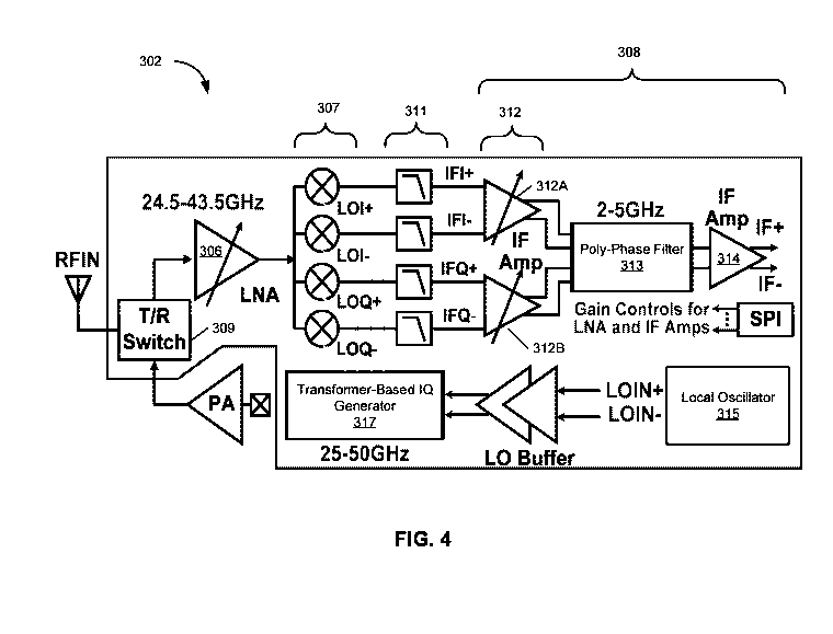
[0035] Figure 4 is a block diagram illustrating an example of an RF
receiver according to
one embodiment. Referring to Figure 4, RF receiver 302 includes, amongst
others, a low-
noise amplifier (LNA) 306 to receive and amplify RF signals, a transformer-
based IQ
generator 317, one or more load resisters (not shown), one or more mixers 307,
and a
downconverter. The transformer-based IQ generator 317 is configured to
generate a
differential in-phase local oscillator (LOT) signal and a differential
quadrature (LOQ) signal
based on a local oscillator (LO) signal received from an LO 315. The load
resisters are
coupled to an output of the transformer-based IQ generator 317. Each of the
load resisters is
configured to couple one of the differential LOT and LOQ signals (e.g., LOI+,
LOT-, LOQ+,
or LOQ- signals in this example) to a predetermined bias voltage (not shown).
The mixers
307 are coupled to the LNA 306 and the transformer-based IQ generator 317 to
receive and
mix the RF signals amplified by the LNA 306 with the differential LOT and LOQ
signals to
down convert the RF signals into IF signals, which can be processed by a
signal processing
module or a signal processor such as a digital signal processor (DSP). In this
embodiment,
the downconverter is represented by a set of low-pass filters 311, a set of
one or more IF
amplifiers 312 (e.g., variable gain amplifiers), a poly-phase filter 313, and
another IF
amplifier 314.
[0036] In this example, there are four mixers coupled to an output of LNA
306 and an
output of transformer-based IQ generator 317. The output of transformer-based
IQ generator
317 includes four LO signals (e.g., LOI+, LOT-, LOQ+, and LOQ- signals) based
on the
original LO signal provided by LO 315 (e.g., LOIN+ and LOIN-). LOI+ and LOT-
represent a
differential in-phase signal and LOQ+ and LOQ- represent a differential
quadrature signal.
LOIN+ and LOIN- represent a differential LO input signal to transformer-based
IQ generator
317. Low-pass filters 311 include four low-pass filters, one for each of
mixers 307 to perform
a low-pass operation on the RF signals from the corresponding mixer to convert
the RF signal
to an IF signal, in this example, IFI+, IFI-, IFQ+, and IFQ- signals. The pair
of IFI+ and IFI-
9
CA 03137133 2021-10-18
WO 2020/214733
PCT/US2020/028361
signals are fed into a differential input of IF amplifiers 312A, while the
pair of IFQ+ and
IFQ- signals are fed into a differential input of IF amplifiers 312B. The
outputs of the IF
amplifiers 312 (collectively represented by IF amplifiers 312A and 312B) are
coupled to an
input of PPF 313. Another IF amplifier 314 is coupled to the output of PPF 313
to further
amplify the IF signals. The amplified IF signals produced by IF amplifier 314
can be
processed further downstream by a signal processor (e.g., DSP or baseband
processor).
[0037] PPF 313 can filter out higher frequency noise and can recombine the
four in-phase
and quadrature signals back into a differential pair of IF signals, e.g.,
IFI+, IFI-, IFQ+, and
IFQ- signals. PPF 313 is a resistive-capacitive capacitive-resistive (RC CR)
PPF. PPF 313
can filter out undesirable signal noise, e.g., high frequency noise outside
the range of the IF
frequencies, and can combine the four in-phase and quadrature signals, e.g.,
IFI+, IFI-, IFQ+,
and IFQ- signals, into a differential pair of intermediate IF signals.
Finally, amplifier 314 to
further amplify the differential intermediate IF signals to generate IF+ and
IF- as an output.
[0038] Figure 5 is a schematic diagram illustrating an example of a
transformer-based IQ
generator according to one embodiment. Referring to Figure 5, according to one
embodiment,
the transformer-based IQ generator 317, also referred to as a transformer-
based IQ network,
includes a positive LOT (LOT+) port to produce an LOI+ signal and a negative
LOT (LOT-)
port to produce an LOT- signal based on LO input signals LOIN+ and LOIN-
generated from
LO 315. The LOI+ and LOT- signals represent a differential in-phase signal, a
positive LOQ
(LOQ+) port to produce an LOQ+ signal, and a negative LOQ (LOQ-) port to
produce an
LOQ- signal. The LOQ+ and LOQ- signals represent a differential quadrature
signal. The
output signals LOI+, LOT-, LOQ+, and LOQ- are provided to inputs of mixers 307
respectively. An example of transformer-based IQ generator 317 is shown in
Figure 7.
[0039] According to one embodiment, a load resister (RI) is coupled between
each of the
output ports (LOT+, LOT-, LOQ+, and LOQ-) and a bias voltage Vbias. By
connecting a load
resister to an output terminal of transformer-based IQ generator 317, the
output impedance
can be increased, which in turn increases the voltage applied to an input of a
mixer. The
higher input voltage will lead to a higher conversion gain of the mixer.
Figure 6 shows a
simulation result of a voltage gain with a load resister from 50 to 500 ohms.
CA 03137133 2021-10-18
WO 2020/214733
PCT/US2020/028361
[0040] Figure 8 is a schematic diagram illustrating a mixer circuit
according to one
embodiment. Referring to Figure 8, mixer 307 is an IQ double balanced mixer,
including a
first mixer 801 and a second mixer 802. A mixer is a three port device that
can perform a
frequency conversion or modulation of a signal. For a receiver, a mixer down
converts (or
demodulates) an RF signal using an LO signal to generate an IF signal. In one
embodiment,
mixers 307 includes two (or double) balanced Gilbert mixers 801 and 802.
Double balanced
mixers 801-802 down convert (or demodulate) a differential RF signal using
differential LO
signals to generate differential IF signals.
[0041] For example, mixer 801 receives a positive RF input signal RF+ and a
negative
RF input signal RF- representing a differential RF signal, for example,
received from LNA
306. The input RF signals RF+ and RF- are mixed with differential in-phase LO
signals (e.g.,
LOI+ and LOT- signals) to generate IFI+ and IFI- signals. The LOI+ and LOT-
signals are
generated by an mm-wave wideband IQ generation circuit, such as IQ generator
317 of
Figure 4. Similarly, mixer 802 receives RF+ and RF- signals and mix with
differential
quadrature LO signals (e.g., LOQ+ and LOQ- signals) generated by a mm-wave
wideband IQ
generation circuit, such as IQ generator 317 of Figure 4, to generate IFQ+ and
IFQ- signals.
In some embodiments, each of mixers 801-802 can include one or more
differential amplifier
stages.
[0042] Referring to Figure 8, for a two stage differential amplifier, the
amplifier can
include a common source differential amplifier as the first stage and a gate-
coupled
differential amplifier as the second stage. The common source differential
amplifier stage of
mixers 801-802 each can receive differential signals RF+ and RF-. The gate-
coupled
differential amplifier stage of mixer 801 receives differential in-phase
signals LOI+ and LOT-
The gate-coupled differential amplifier stage of mixer 802 receives
differential quadrature
signals LOQ+ and LOQ-. The RF signal is then down converted by the LO signal
to generate
an IF signal. The second stage can include a low-pass filter which can be
first order low-pass
filters to minimize high frequency noise injections into mixers 801-802. In
one embodiment,
the low-pass filter includes a passive low pass filter having a load resistor
in parallel with a
capacitor. In one embodiment, the first stage different amplifier is coupled
to the second stage
11
CA 03137133 2021-10-18
WO 2020/214733
PCT/US2020/028361
differential amplifier via differential inductors. In one embodiment, mixers
801-802 is co-
designed with a mm-wave IQ generation circuit such as mm-wave IQ generation
circuit 317
of Figure 4 on a single monolithic integrated circuit. In one embodiment, a
differential
inductor pair can be used to pick up a current gain between the two
differential amplifier
stages. Four inductors are included for better performance, e.g., two
differential inductor
pairs are used for each of the double IQ mixers. Four inductors, however,
include a large foot.
[0043] Figure 9 is a schematic diagram illustrating a co-design of T/R
switch 309 and
LNA 306 with impedance matching network to further improve the performance.
LNA 306 is
designed with different resonant loads in two stages to serve as a wideband
frontend. To
mitigate the loading effect of the parasitic capacitors from T/R switch 309
and the off-state
PA, separate shunt inductors are applied to the TX/RX inputs. The RX input
shunt inductor
LR)( is further co-designed with Lg, Ls, and Cgs of the first stage LNA, which
creates a high-
order network for wideband input marching.
[0044] In the foregoing specification, embodiments of the invention have
been described
with reference to specific exemplary embodiments thereof It will be evident
that various
modifications may be made thereto without departing from the broader spirit
and scope of the
invention as set forth in the following claims. The specification and drawings
are,
accordingly, to be regarded in an illustrative sense rather than a restrictive
sense.
12