Note : Les descriptions sont présentées dans la langue officielle dans laquelle elles ont été soumises.
CA 03137343 2021-10-19
WO 2020/227785
PCT/AU2020/050488
IMPROVED REFLECTION MODE DYNODE
FIELD OF THE INVENTION
[001]. The present invention relates to electron emissive surfaces capable
of releasing
electrons in response to impact by a particle including an ion, a neutral
atom, a neutral
molecule, a proton, a neutron, an electron or a photon. These surfaces may be
used to
convert, for example, an ion into an electron signal, or an electron signal
into an amplified
electron signal. The invention is particularly applicable to conversion or
amplification
dynodes.
BACKGROUND TO THE INVENTION
[002]. In many scientific applications, it is necessary to detect an ion, a
neutral atom, a
neutral molecule, a proton, a neutron, an electron or a photon. Typically, a
detector is
comprised of a first conversion surface (dynode), with which an incident
particle collides
and emits secondary electrons that are subsequently amplified in a multiplying
section.
Alternatively, the first conversion surface can emit particles other than
electrons that
interact with a send conversion surface, and that second conversion surface
emits
secondary electrons that are subsequently amplified in a multiplying section
of the detector.
[003]. The multiplying section of a detector generally operates by way of
secondary
electron emission whereby the impact of a single or multiple particles on the
multiplier
impact surface causes single or (preferably) multiple electrons associated
with atoms of the
impact surface to be released. Generally, the multiplying section comprises a
chain of
dynodes, each of which sequentially amplifies the electron signal of the
dynode before it
in the chain.
1
CA 03137343 2021-10-19
WO 2020/227785
PCT/AU2020/050488
[004]. A practical example of the use of electron emissive surfaces is in
ion detectors as
used in a mass spectrometers. In mass spectrometers, the analyte is ionized to
form a range
of charged particles (ions). The resultant ions are then separated according
to their mass-
to-charge ratio, typically by acceleration and exposure to an electric or
magnetic field. The
separated signal ions impact on an ion detector surface (which is electron
emissive) to
generate one or more secondary electrons. These secondary electrons are then
directed
toward a dynode chain that functions to significantly multiply the electron
signal generated
by the ion detector conversion surface. The electron signals output by the
electron
multiplier are displayed as a spectrum of the relative abundance of detected
ions as a
function of the mass-to-charge ratio.
[005]. The detection efficiency (or sensitivity) of electron multipliers is
in part limited by
the statistics of secondary electron generation upon particle (ion) impact
with a surface.
Due to the statistical nature of secondary electron generation, surfaces
comprised of a
relatively low average secondary electron yield material have a high rate of
non-emission
events leading to non-detection or false-negative results. In contrast, a
higher average
secondary electron yield material has a lower rate of non-emission, which
leads to higher
detection efficiencies.
[006]. Sensitivity of detectors is a core performance specification and
accordingly artisans
in this field continually seek improvements in materials and construction so
as to maximize
the yield of secondary electrons from electron emissive surfaces. The industry
standard for
sensitivity has not changed in some decades, and it is against this general
lack of success
that the present invention is provided.
[007]. A further problem in the art is electron emissive surfaces may
accumulate charge
under higher levels of irradiation. This accumulation of charge may arise from
the
integration of incident charge as well as the emission of secondary electrons,
resulting in
an uncontrolled change of electrical potential at the conversion surface and
ultimately
leading to failure of the detector.
2
CA 03137343 2021-10-19
WO 2020/227785
PCT/AU2020/050488
[008].
It is an aspect of the present invention to provide an improvement in
secondary
electron yield from emissive surfaces. It is a further aspect of the prior art
to provide a
useful alternative to prior art electron emissive surfaces.
[009]. The
discussion of documents, acts, materials, devices, articles and the like is
included in this specification solely for the purpose of providing a context
for the present
invention. It is not suggested or represented that any or all of these matters
formed part of
the prior art base or were common general knowledge in the field relevant to
the present
invention as it existed before the priority date of each claim of this
application.
SUMMARY OF THE INVENTION
[010]. After considering this description it will be apparent to one
skilled in the art how
the invention is implemented in various alternative embodiments and
alternative
applications. However, although various embodiments of the present invention
will be
described herein, it is understood that these embodiments are presented by way
of example
only, and not limitation. As such, this description of various alternative
embodiments
should not be construed to limit the scope or breadth of the present
invention. Furthermore,
statements of advantages or other aspects apply to specific exemplary
embodiments, and
not necessarily to all embodiments (or even any embodiment) covered by the
claims.
[011]. Throughout the description and the claims of this specification the
word "comprise"
and variations of the word, such as "comprising" and "comprises" is not
intended to exclude
other additives, components, integers or steps.
[012]. Reference throughout this specification to "one embodiment" or "an
embodiment"
means that a particular feature, structure or characteristic described in
connection with the
embodiment is included in at least one embodiment of the present invention.
Thus,
appearances of the phrases "in one embodiment" or "in an embodiment" in
various places
3
CA 03137343 2021-10-19
WO 2020/227785
PCT/AU2020/050488
throughout this specification are not necessarily all referring to the same
embodiment, but
may.
[013]. In a first aspect, but not necessarily the broadest aspect, the
present invention
provides a device configured to convert or amplify a particle, the conversion
or
amplification being reliant on the impact of a particle on a surface of the
device causing
the emission of one or more secondary electrons from the same surface, wherein
the device
comprises a carbon-based layer capable of secondary electron emission upon
impact of a
particle.
[014]. Applicant has unexpectedly found significant practical advantage in
the use of
carbon-based layers (such as diamond films) as an electron emissive layer for
a reflection
mode dynode. Particularly, it is proposed that the sensitivity of electron
multiplication
detection systems is improved by the use of a substantially continuous film of
diamond that
is doped or otherwise configured to be sufficiently electrically conductive
for use as a
reflection mode dynode.
[015]. In one embodiment of the first aspect, the device is configured as a
conversion
dynode or an amplification dynode or a microchannel wafer or a microchannel
plate.
[016]. In one embodiment of the first aspect, the conversion dynode or
amplification
dynode is configured to operate in reflection mode. As will be appreciated
reflection mode
devices are structurally and functionally distinguished from devices dedicated
to operating
in transmission mode. A reflection mode device is configured such that a
single face of
the device both receives an incident particle and emits the resultant
secondary electrons.
By contrast, a device which operates in transmission mode has a first face
which receives
an incident particle, and a second face which emits the resultant secondary
electrons.
[017]. The structural and functional differences between reflection and
transmission mode
devices known at the present filing date inform as to the structural and
functional features
of the present devices (being directed to reflection mode devices) that may
distinguish from
4
CA 03137343 2021-10-19
WO 2020/227785
PCT/AU2020/050488
transmission mode devices. Any of these distinguishing features may constitute
a feature
of the present reflection mode devices.
[018]. One difference between these two modes are the thickness of the
dynodes. In
reflection mode, the thickness of the emission layer is typically in the
micron order or
larger. However, in transmission mode, much thinner dynodes are required to
obtain a
useful secondary electron yield. Reflection-type dynodes are not constrained
by a
maximum thickness of the diamond-based material, thereby relaxing the degree
of
manufacturing control required in their manufacture. Furthermore, reflection
dynodes can
be manufactured on a non-planar substrate to conveniently enable electrical
field design
conducive to focussing dynodes.
[019]. In one embodiment of the first aspect, the carbon-based layer is a
diamond layer or
a diamond-like carbon layer. As used herein, the term "diamond" includes the
diamond
allotrope of pure carbon, being carbon atoms bonded into a tetrahedral network
via sp3
orbitals. As will be detailed infra, a diamond layer may be doped with an
impurity to
increase electrical conductivity, and in that regard would not be considered a
"pure"
diamond. Although less prefen-ed, undoped diamond may be used where it is
formed in a
manner that confers some conductivity on the substance (one example being
formation by
chemical vapour deposition).
[020]. It is contemplated that the carbon-based layer may be formed from a
diamond-like
carbon. As known to the skilled artisan diamond-like carbon materials comprise
appreciable levels of sp3 hybridised carbon atoms, and accordingly these
materials have
many similarities to the diamond allotrope of pure carbon having purely sp3
bonding. Some
forms of diamond-like carbon are capable of emitting secondary electrons,
tetrahedral
amorphous carbon (ta-C) being one such example.
[021]. In one embodiment of the first aspect, the carbon-based layer is
doped to confer or
increase conductivity. The carbon based layer may have zero or low levels of
conductivity
which may be improved by the introduction of a dopant during formation of the
layer. The
5
CA 03137343 2021-10-19
WO 2020/227785
PCT/AU2020/050488
dopant atom substitutes for carbon in the diamond lattice, thereby donating a
hole into the
valence band. The level of dopant used may be an-ived at by the skilled person
having
regard to the final electrical conductivity required for the material to
function efficiently as
an electron emissive surface.
[022]. The dopant type and concentration alters the transport of secondary
electrons
through the layer bulk, in addition to the electrical conductivity required to
replace the
secondary electrons emitted. In one embodiment of the first aspect, the dopant
is a p-type
dopant (preferably boron), but may in other embodiments be n-type (such as
nitrogen).
The dopant may be boron or nitrogen, but is preferably boron. Where boron is
the dopant,
concentrations of greater than 1019 cm-3 may be useful in the context of a
reflection mode
dynode. Greater levels of electrical conductivity will be seen where boron is
used at a
concentration of greater than 1020 cm-3, or greater than 1021 cm-3, or greater
than 1022 cm-
3. In some embodiments of the invention, an undoped diamond material may be
used, as
further described infra.
[023]. In one embodiment of the first aspect, the carbon-based layer has a
crystalline
structure. For example, the layer may have a polycrystalline, nano-
crystalline, ultra-nano-
crystalline, or single crystalline structure. In one embodiment of the
invention, the layer
comprises grain sizes at the nano- (1 to 100 nm) and/or ultra-nano (less than
5 nm) scales.
[024]. Layers having useful properties are proposed to be polycrystalline
diamond having
an average or median grain size of between about 1 nm and about 1000 nm. In
the
exemplary embodiments disclosed herein, grain sizes of around 1 nm were shown
to be
useful. As will be appreciated, given the heterogenous nature of
polycrystalline materials
a range of grain sizes will be found in any given sample. In other
embodiments, median
grain size may be greater than about 1 nm, and may be up to about 10 nm, 20
nm, 30 nm,
40 nm, 50 nm, 60 nm, 70 nm, 80 nm, 90 nm or 100 nm.
[025]. It is proposed that ultra-nanocrystalline diamond (having a grain
size of a less than
about 5, 4, 3, 2 or 1 nm in some embodiments) may be particularly useful in
the context of
6
CA 03137343 2021-10-19
WO 2020/227785
PCT/AU2020/050488
the present invention given that a layer fabricated from such material may be
sufficiently
conductive so as to provide an electron emissive surface. Diamond is a wide
band-gap
semiconductor, and is intrinsically electrically insulating. It is proposed
that a film of ultra-
nanocrystalline diamond is sufficiently thin so as to allow for quantum
tunneling to enable
sufficient electrical conductivity to mitigate charging effects. The use ultra-
nano
polycrystalline diamond may therefore reduce or negate the need for a dopant
thereby
simplifying and/or reducing the cost of manufacture.
[026]. In one embodiment of the first aspect, the carbon-based layer has a
minimum
thickness to prevent or inhibit the passage of high energy particles
therethrough. As will
be appreciated, there will be a general preference for avoiding a particle
incident on the
carbon-based layer from not travelling the depth from which any secondary
electrons that
are generated may escape from the incident surface. A particle passing
completely through
the layer may not emit the maximum number of secondary electrons that would
otherwise
be achievable. As will be further appreciated, the penetration distance will
not be a single
value and instead a distribution of distances will be expected. In that
regard, a mean or
median penetration distance may be considered when determining the required
depth of
the carbon-based layer. In addition or alternatively, the thickness may be a
minimum
thickness providing for a required secondary electron yield.
[027]. To ensure that all, or almost all incident particles are captured in
the layer, the layer
depth may be set by reference to a multiple of the mean or median depth of
penetration. In
that regard, a multiple of 1.5, 2, 2.5, 3, 3.5, 4, 4.5, 5, 5.5, 6. 6.5, 7,
7.5, 8, 8.5, 9, 9.5, 10,
15, 20, 20, 25, 30, 35, 40, 45, 50, 55,60, 65, 70, 75, 80, 85, 90, 95 or 100
may be used. An
appropriate multiple may be informed by a consideration of the range of
penetration
distances within the distribution; a lesser distance range informing of a
lesser multiple and
vice versa.
[028]. The carbon-based layer may be of any thickness, however maximum
thickness may
be dictated by ease of fabrication or considerations of economy.
7
CA 03137343 2021-10-19
WO 2020/227785
PCT/AU2020/050488
[029]. In one embodiment of the first aspect, the carbon-based layer has a
thickness of less
and about 5 nm, or less than about 1 nm, or between about 1 nm and about 500
nm, or
between about 1 nm and about 100 nm. Where the carbon-based layer is formed
from
nanocrystalline diamond, the layer thickness may be greater than 10 nm.
[030]. In one embodiment of the first aspect, the carbon-based layer is
formed by a growth
process on a substrate. In the context of the present invention, the term
"growth" means
that the layer is not preformed separately and then applied to the substrate.
Instead, the
carbon-based layer is grown on the substrate in situ, such that the thickness
of the layer
increases during the growing process.
[031]. In one embodiment of the first aspect, the growth process is a
deposition process.
For example, growth may be achieved by a vapour deposition process. This
method is
reliant on the coating material being presented to the substrate in a vapour
state and
deposited via condensation, chemical reaction, or conversion. Examples of
vapour
deposition methods include physical vapour deposition (PVD) and chemical
vapour
deposition (CVD). hi PVD, the substrate is subjected to plasma bombardment. h)
CVD,
thermal energy heats gases in a coating chamber, driving the deposition
reaction. Vapour
deposition methods are usually performed within a vacuum chamber.
[032]. In one embodiment of the first aspect, the vapour deposition method
is a physical
vapour deposition method, which may be a plasma-based method, or a sputtering
method
(such as a high power impulse magnetron sputtering method).
[033].
Physical vapour deposition methods are typically reliant on dry vacuum
deposition
in which a coating material is deposited over the substrate. Reactive PVD hard
coating
methods generally require a method for depositing the material, an active gas
(such as
nitrogen, oxygen, or methane), and plasma bombardment of the substrate.
[034].
Sputtering alters the physical properties of a surface. In this process, a gas
plasma
discharge is provided between a cathode coating material and an anode
substrate.
8
CA 03137343 2021-10-19
WO 2020/227785
PCT/AU2020/050488
Positively charged gas ions are accelerated into the cathode. The impact
displaces atoms
from the cathode, which then impact the anode and coat the substrate. A film
forms on the
substrate as atoms adhere to the substrate. Three techniques for sputtering
are available to
the skilled person for potential use in the present invention: diode plasmas,
RF diodes, and
magnetron-enhanced sputtering.
[035]. The steps in a typical CVD process are as follows: generation of the
reactive gas
mixture, transport of reactant gas to the surface to be coated, adsorption of
the reactants on
the surface to be coated, and reaction of the adsorbents to form the coating.
[036]. To explain further, the reactant gas mixture is contacted with the
substrate. The
coating material is delivered by a precursor material (termed a reactive
vapour) which may
be dispensed as a gas, liquid, or in solid phase. The gases are fed into a
chamber under
ambient pressures and temperatures while solids and liquids are provided at
high
temperature and/or low pressure. Once resident in the chamber, energy is
applied to the
substrate surface to facilitate the coating reaction with the can-ier gas.
[037]. Pre-treatment of the substrate surface is generally required in
vapour deposition
methods, and particularly in CVD. Mechanical and/or chemical means may be used
before
the substrate enters the deposition reactor. Cleaning is typically effected by
ultrasonic
cleaning and/or vapour degreasing. To facilitate adhesion of the coating,
vapour honing
may be used. During the coating process, surface cleanliness is maintained to
prevent
particulates from entering in the coating. Mild acids or bases may be used to
slough oxide
layers which may have formed during the heat-up step. Post-treatment of the
coating may
include exposure to heat to cause diffusion of the coating material across the
surface.
[038]. In the exemplary embodiment, CVD was implemented in the presence of
a
hydrogen plasma so as to inhibit growth of graphitic carbon bonds. Nanodiamond
particles
were firstly dispersed onto the substrate, and the polydiamond grown from the
particles.
9
CA 03137343 2021-10-19
WO 2020/227785
PCT/AU2020/050488
[039]. In one embodiment of the first aspect sputtering may itself be used
to deposit the
coating material, and not necessarily in the context of any vapour deposition
process.
[040]. In one embodiment of the first aspect, the coating material is
deposited on the
substrate surface by a thermal spray method, including a combustion torch
method, a flame
spraying method, a high velocity oxy fuel method, a detonation gun method, an
electric arc
spraying method and a plasma spraying method. Nanocrystalline-diamond
particles may
be produced in the form of a coating by depositing Ni-clad graphite powder in
a high-
velocity thermal spray method. Particles are accelerated to impact and form a
film on a
metal substrate. Electron microscopy reveals that the deposited layer contains
cubic
diamond nanocrystals having a size range of 5 to 10 nm.
[041]. There exists three basic categories of thermal spray technologies:
combustion torch
methods (including flamespray, high-velocity oxy fuel, and detonation gun
methods),
electric (wire) arc methods, and plasma arc methods.
[042]. Flame spraying methods involve feeding gas and oxygen through a
combustion
flame spray torch. The layer material is fed into the flame. The layer
material is heated to
about or higher than its melting point, and then accelerated by combustion of
the layer
material. The so-formed molten droplets flow on the surface to form a
continuous and even
coating.
[043]. High-velocity oxy fuel (HVOF) methods require the layer material to
be heated to
a temperature of about or greater than its melting point, and then deposited
on the substrate
by a high-velocity combustion gas stream. The method is typically canied out
in a
combustion chamber to enable higher gas velocities. Fuels used in this method
include
hydrogen, propane, or propylene.
[044]. Plasma spraying relies on introduction of a flow of gas (typically
argon) between a
water-cooled anode and a cathode. A direct cun-ent arc passes through the gas
stream
CA 03137343 2021-10-19
WO 2020/227785
PCT/AU2020/050488
causing ionization and the formation of a plasma. The plasma heats the layer
material (in
powder form) to a molten state. Compressed gas directs the material onto the
substrate.
[045]. Other methods of diamond growth include high pressure high
temperature (HPHT);
detonation; and ultrasound cavitation methods.
[046]. Conventional liquid handling and/or spraying techniques may be used
to deposit a
nanodiamond sluny (including an ultra-nanodiamond slurry) may be deposited.
Such
approaches have the advantage of simplicity and a lower capital cost given
that only
relatively basic equipment is required. Moreover, a nanodiamond slurry may be
purchased
from a third party supplier, and in litre volumes for very low cost. Only
several mL of a
slurry is required to cover a growth area of around 8,000 mm2, such an area
being typical
of a production scale used for the commercial manufacture of an electron
emissive surface.
There is no vacuum chamber, special deposition process or incremental growth
required.
An electron emissive surface may be provided by simply applying an even layer
of
nanodiamond sluny onto a substrate. Such application is significantly more
rapid than the
slower incremental growth methods disclosed elsewhere herein.
[047]. The nanodiamond slurry may comprise a doped diamond as discussed
elsewhere
herein, including a boron doped diamond. An electron multiplier having
electron emissive
surfaces formed from a nanodiamond slurry may comprise only a portion dynodes
formed
in this manner. Particularly, in some embodiments dynode(s) involved only in
ion-to-
electron conversion and/or only the first 1, 2, 3, 4 or 5 dynode(s) of an
electron
multiplication chain may be formed from nanodiamond, the remainder dynodes
being
otherwise fabricated whether or not having a carbon-based surface. Use of
nanodiamond
in this manner may provide for enhanced sensitivity and/or improved pulse
height
distributions over prior art multipliers, such enhancements and improvements
being
achievable in an exceedingly economical way.
[048]. In one embodiment of the first aspect, the carbon-based layer formed
by growth on
a substrate is subjected to post-growth modification. The modification may be
effected to
11
CA 03137343 2021-10-19
WO 2020/227785
PCT/AU2020/050488
improve any mechanical, physical, chemical, electrical, thermal, or other
property of the
grown layer as required or desired. In one embodiment of the first aspect, the
post-growth
modification creates a negative electron affinity of at least a portion of the
carbon atoms of
the carbon-based layer. A very low or even negative electron affinity at the
layer surface
permits low-energy quasithermalized electrons to reach the surface and escape
into the
sun-ounding vacuum.
[049]. In one embodiment of the first aspect, the post-growth modification
causes
termination of the carbon atoms of the carbon-based layer. The termination may
be effected
by hydrogen, fluorine or an alkali earth metal such as caesium. As will be
appreciated,
some termination atoms will be prefen-ed over others when having regard to the
desired
end result of increasing the negative electron affinity of the layer surface.
[050]. Preferably the surface of the layer is substantially saturated with
the termination
atom.
110511 After chemical vapour deposition of diamond, the (100) and
(111) surfaces may be
naturally terminated by hydrogen at least to some extent, and accordingly no
specific steps
need be taken to effect termination.
[052]. However, where termination is required (or greater levels of
termination are
desired) then active steps may be taken to effect termination. For example,
where hydrogen
termination is required this is often has been achieved using atomic hydrogen
produced by
either plasma or hot filament techniques as known to the skilled artisan. In
one embodiment
of the first aspect, the post-growth modification is by exposure of the carbon-
based layer
to a gas plasma (typically hydrogen gas).
[053]. Alternative methods use high temperature molecular hydrogen to
hydrogenate the
surface of diamond films, even at atmospheric pressure. Hydrogen termination
of chemical
vapour deposited diamond films may be due to the formation of surface carbon
dangling
12
CA 03137343 2021-10-19
WO 2020/227785
PCT/AU2020/050488
bonds and carbon-carbon unsaturated bonds at the applied temperature, which
are reactive
with molecular hydrogen to produce a hydrogen-terminated surface.
[054]. Generally, hydrogen surface termination will be necessary or at
least preferred for
nano and ultra-nano diamond materials to confer sufficient conductivity for
use in the
context of the present invention.
[055].
The present device may comprise a substrate which, at least in part, acts to
support the
electron emissive layer. Where the electron emissive layer is exceedingly
thin, mechanical
support may be required. The substrate may provide other structural or
functional effects.
[056]. While non-conductors (such as silicon) are capable of having
microcrystalline
diamond layered thereon, for applications in electron multipliers electrical
conductivity is
required. In that regard, a non-conducting substrate such as silicon may
nevertheless be
used, and the carbon-based layer electrically connected to a power source.
[057]. In one embodiment of the first aspect, the substrate is a metal or
metal alloy such
as nickel or steel. The use of more exotic metals and alloys may provide
advantage.
[058]. In one embodiment of the first aspect, the metal is a transition
metal, and may be a
second row or third row transition metal such as molybdenum, or tungsten.
Molybdenum
was utilised as a substrate in the exemplary embodiments given its high
melting point and
low thermal coefficient of expansion.
[059]. Where a diamond material is applied to the substrate in the form of
a slurry, the
diamond material may naturally engage with substrate upon removal of the
slurry solvent.
In addition or alternatively, sonication of a substrate while contacted with a
dense sluny
may lead to sufficient engagement between the substrate and diamond material.
Alternatively a binder, an adhesive or an encapsulation material may be
applied about or
over the diamond material such that the diamond material is electrically
contacted (and
13
CA 03137343 2021-10-19
WO 2020/227785
PCT/AU2020/050488
contact maintained) with the substrate although there is little or no actual
chemical or
physical engagement between the two.
[060]. The present devices may be used in any useful context, such as to
convert an
incident (non-electron or electron) particle into one or more secondary
electrons.
[061]. The devices of the present invention may provide a secondary
electron yield of at
least 1, 2, 3, 4, 5, 6, 7, 8, 9, 10, 11, 12, 13, 14, 15, 16, 17, 18, 19, 20,
21, 22, 23, 24, 25, 26,
27, 28, 29, 30, 31, 32, 33, 34, 35, 36, 37, 38, 39, 40, 41, 42, 43, 44, 45,
46, 47, 48, 49, 50,
51, 52, 53, 54, 55, 56, 57, 58, 59, 60, 61, 62, 63, 64, 65,66, 67,68, 69, 70,
71, 72, 73, 74,
75, 76, 77, 78, 79, 80, 81, 82, 83, 84, 85, 86, 87, 88, 89, 90, 91, 92, 93,
94, 95, 96, 97, 98,
99, or 100 electrons. In preferred forms of the invention yields of at least
5, 10 or 15
electrons for incident electron energies in the range of about 200 to about
1000 are provided
[062]. In a second aspect, the present invention provides an electron
multiplier comprising
one or more devices of any embodiment of the first aspect.
[063]. With regard to applications of the present reflection mode devices
for use in a
discrete dynode electron multiplier, it is contemplated that not all dynodes
in the
amplification chain of the multiplier will benefit equally from the use of a
carbon-based
coating (as compared with another coating). As will be clear from the
comparative data
shown in FIG. 4 (the generation of which is disclosed in greater detail
infra), no significant
advantage in terms of secondary electron yield for the present invention is
noted for
electron energies of up to about 100 eV, with the present devices being
superior in terms
of yield at higher energies.
[064]. Apart from secondary electron yield, use of a carbon-based layer on
a dynode may
provide advantage in that contaminant species may be less likely to adsorb
thereon,
providing greater stability or a longer service life. Furthermore, a carbon-
based layer may
be less susceptible to deterioration by corrosive chemicals such as chlorine
and fluorine.
14
CA 03137343 2021-10-19
WO 2020/227785
PCT/AU2020/050488
[065]. As another possibility, a device of the present invention may be
used only as a
conversion dynode within a detector, with the multiplying dynodes being all
standard
dynodes. h) this way, an improved yield of secondary electrons (compared with
a prior art
conversion dynode) is obtained only at the conversion dynode, with the
remainder of the
multiplier being standard.
[066]. In general terms, the advantage to using the present devices in only
some dynodes
may be economic given the likely lower cost of standard dynodes.
1 0 [067]. In
general regard to the application of the present invention to electron
multipliers,
with the exception of any reflection dynode(s) used the multiplier may be
configured in
accordance with the prior art. As is conventional in an electron multiplier, a
first electron
emissive surface (of the first dynode in a series of dynodes) is provided
which is configured
to receive an input particle, and in response to the impact of the input
particle emit one or
multiple electrons. Where multiple electrons are emitted (which is typical),
an
amplification of the input signal results. As is also conventional, a series
of second and
subsequent electron emissive surfaces is provided. The function of these
emissive surfaces
is to amplify the electron(s) which are emitted from the first emissive
surface. As will be
appreciated, amplification occurs typically at each subsequent emissive
surface of the
series of emissive surfaces. Typically, the secondary electrons emitted by the
final
emissive surface are directed onto an anode surface, with the cun-ent formed
in the anode
feeding into a signal amplifier and subsequently an output device.
[068].
Reference is made to FIG. 5 showing an exemplary form of an electron
multiplier.
With an electron multiplier, a linear path is defined between opposing dynodes
as shown
in FIG. 5, being a highly diagrammatic representation of the dynodes of a
conventional
discrete dynode electron multiplier (100). Each of the dynodes in the electron
amplification chain are sequentially numbered (115a through 115g). Any one or
more of
the dynodes (115) may be a dynode of the present invention. The path of an
incoming
particle (120) is shown at the entry of the multiplier (10), with the
subsequent amplification
leading to an avalanche of electrons (125).
CA 03137343 2021-10-19
WO 2020/227785
PCT/AU2020/050488
[069]. In the context of an electron multiplier, the present invention may
provide
advantage in that a reflection mode dynode or series of reflection mode
dynodes may be
operated at a lower voltage, thereby providing extra voltage overhead for a
longer service
life whilst not compromising on secondary electron yield.
[070]. Given the increase in secondary electron yield available by way of
the present
invention, an electron multiplier may comprise less than the conventional
number of
dynodes. For example, a prior art multiplier having 12 dynodes may function
acceptably
using only 6 of the present dynodes if each of the present dynodes has a two-
fold secondary
electron yield compared with the prior art dynode, and where the secondary
electron yield
of the prior art material is equal to or less than two. The use of lower
dynode numbers
allows for an amplifier to be constructed with a smaller volume, a lighter
weight, more
simply, using less materials, using a smaller number of components, or at a
lower cost.
[071]. Dynodes having a carbon-based layer may have another advantage in
that an
increased chemical inertness could confer utility in the detection of reactive
species that
would otherwise degrade a prior art dynode.
[072]. The
present invention has particular applicability in the context of mass
spectrometers, which typically utilize discrete dynode electron multipliers
whereby the
dynodes of the multiplier operate in reflection mode. In that regard, the
present invention
provides as a third aspect a mass spectrometer comprising one or more devices
of any
embodiment of the first aspect, or an electron multiplier of the second
aspect.
[073].
Apart from inclusion of the present devices, the mass spectrometer may be
otherwise constructed conventionally, as illustrated in FIG. 6 showing a mass
spectrometer
in combination with a gas chromatography system.
[074]. The
present invention may be embodied in a third aspect, being a method of
fabricating an electron emissive device operable in reflection mode. It will
be understood
16
CA 03137343 2021-10-19
WO 2020/227785
PCT/AU2020/050488
that in describing the device aspects of the present invention, various
features relating to
methods for fabrication are discussed. So far as they are applicable to a
method of
fabrication, features described with reference to the present devices are
incorporated herein
by reference to the following discussion of the present methods. For example,
features of
post-growth modification of the carbon-based layer are used herein to
characterize the
device per se, however such features may also be applicable to the present
methods.
[075]. The third aspect of invention, may in particular, provide a method
for fabricating a
device configured to convert or amplify a particle, the conversion or
amplification being
reliant on the impact of a particle on a surface of the device causing the
emission of one or
more secondary electrons from the same surface, the method comprising the
steps of
providing a substrate, and forming a carbon-based layer on the substrate.
[076]. In one embodiment of the third aspect, the substrate is suitable for
use in a reflection
mode dynode or microchannel wafer or a microchannel plate.
[077]. In one embodiment of the third aspect, the dynode is a conversion
dynode or an
amplification dynode or a microchannel wafer or a microchannel plate.
[078]. In one embodiment of the third aspect, the carbon-based layer is a
diamond layer
or a diamond-like carbon layer.
[079]. In one embodiment of the third aspect, the carbon-based layer is
formed with a
dopant to increase conductivity. Optionally the dopant is boron.
[080]. In one embodiment of the third aspect, the carbon-based layer is
formed as a
monocrystalline diamond layer.
[081]. In one embodiment of the third aspect, the carbon-based layer is
formed so as to
have a minimum thickness to provide for a required secondary electron yield.
17
CA 03137343 2021-10-19
WO 2020/227785
PCT/AU2020/050488
[082].
In one embodiment of the third aspect, the carbon-based layer is formed to
have a
thickness of less and about 5 nm, or less than about 1 nm, or between about 1
nm and about
500 nm, or between about 1 nm and about 100 nm.
[083]. In one
embodiment of the third aspect, the carbon-based layer is formed by a growth
process on the substrate. Optionally the growth process is a deposition
process, such as a
vapour deposition process.
[084]. In one embodiment of the third aspect, the carbon-based layer formed
by growth
on the substrate is subjected to a post-growth modification step. Optionally
the post-growth
modification step increases the negative electron affinity of at least a
portion of the carbon
atoms of the carbon-based layer. The post-growth modification step may cause
termination
(such as hydrogen termination) of at least a portion of the carbon atoms of
the carbon-based
layer.
[085]. In one embodiment of the third aspect, the post-growth modification
step is by
exposure of the carbon-based layer to a gas plasma. Optionally the gas plasma
is generated
from hydrogen gas, which may be heated hydrogen gas.
[086]. In one
embodiment of the third aspect, the substrate is a metal, and optionally a
transition metal. The transition metal may be a second row or third row
transition metal,
optionally the second row transition metal being molybdenum, or the third row
transition
metal being tungsten.
BRIEF DESCRIPTION OF THE FIGURES
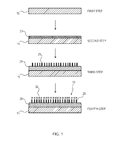
[087].
FIG. 1 is a highly schematic diagram illustrating the steps involved in the
fabrication of a reflection mode dynode of the present invention.
18
CA 03137343 2021-10-19
WO 2020/227785
PCT/AU2020/050488
[088]. FIG. 2 is a series of scanning electron micrographs showing the
surface of a boron-
doped polycrystalline diamond grown on a molybdenum substrate. Panels (a) and
(b) are
micrographs taken at 0 tilting angle. Panels (c) and (d) are micrographs
taken at 450 tilting
angle. Scale bar = 10 nm.
[089]. FIG. 3 is a series of atomic force microscopy images of a boron-
doped
polycrystalline diamond grown on a molybdenum substrate. Two different regions
were
imaged. Panels (a) and (b) are directed to a first region, and panels (c) and
(d) to a second
region. The panels (b) and (d) are three dimensional representations of the
topographic
images of panels (a) and (c) respectively. Scale bar = 5 nm.
[090]. FIG. 4 is a graph comparing the secondary electron yield of a device
of the present
invention (produced in accordance with the illustrative embodiment described
herein)
compared to a prior art device. Both devices were operated in reflection mode.
[091]. FIG. 5 is a highly schematic diagram showing the generation of a
secondary
electron avalanche in a prior art electron multiplier.
[092]. FIG. 6 is a highly schematic block diagram showing a typical
arrangement whereby
a gas chromatography instrument is coupled to a mass spectrometer, the mass
spectrometer
having an ion detector/electron multiplier having at least one dynode having a
carbon-
based layer functioning as an electron emissive material.
DETAILED DESCRIPTION OF ILLUSTRATIVE EMBODIMENTS
[093]. The invention will be further described by reference to a highly
preferred
embodiments with regard to the device and method used to fabricate the device.
It is
emphasised that the embodiments in this section are strictly non-limiting in
scope.
19
CA 03137343 2021-10-19
WO 2020/227785
PCT/AU2020/050488
[094]. With regard to the highly prefen-ed method, reference is made
to FIG. 1 which
illustrates highly diagrammatically the fabrication of a dynode (10) operable
in reflection
mode.
[095]. The first step is the provision of a substrate (15) which in
this embodiment is
molybdenum having a planar upper surface of dimension 50 mm x 50 mm and a
thickness
of 1 mm. The substrate was cleaned by sonication followed by exposure to
oxygen plamsa.
After cleaning, the planar upper surface was spin coated with nanodiamond
particles.
[096]. The second step is the commencement of growing a boron-doped
polycrystalline
diamond film (20) on one face of the substrate (15). The film was deposited by
a plasma
assisted chemical vapour deposition method (PA-CVD), at a pressure of 70 Ton,
with a
microwave power of 900 Watts, and at a temperature of 700 C to 1000 C. During
growth,
gases were introduced into the pressurised chamber at predetermined flow rates
as tabled
below.
Step Time Pressure Heater Power H2 0H4 B(01-
13)3 02
(min) (Torr) (Deg. C) (Watts) (SCCM ) (SCCM )
(SCCM ) (SCCM )
1 0.5 10 0 0 100 1 0 0
2 0.5 10 300 0 100 1 0 0
3 0.2 10 300 400 100 1 0 0
4 0.2 10 300 500 100 1 0 0
5 0.2 10 300 600 150 2 0 0
6 0.5 20 300 700 200 2.5 0 0
7 0.5 30 300 1000 250 3 0 0
8 0.5 30 400 900 300 3 0 0
9 5 60 500 900 300 3 0 0
10 480 70 500 900 100 4 5 0.3
11 480 70 600 900 100 4 5 0.3
12 240 70 600 900 100 4 5 0.3
13 180 70 600 900 100 4 5 0.3
14 360 70 600 900 100 4 5 0.3
15 480 80 600 900 100 4 5 0.3
16 480 90 700 1200 300 2.5 0.15 0
17 10 90 700 1100 300 2.5 0.15 0
18 2 40 700 1000 300 0 0 0
19 2 40 0 0 250 0 0 0
20 2 30 0 0 250 0 0 0
CA 03137343 2021-10-19
WO 2020/227785
PCT/AU2020/050488
21 2 20 0 0 150 0 0
0
22 2 10 0 0 100 0 0
0
23 25 80 0 0 300 0 0
0
[097]. With reference to the above table, growth of the diamond layer
occurs from step 10
to step 15.
[098]. Growth of the film (in terms of depth) continues until the required
depth is
achieved, as shown in the third step. In this embodiment, a film thickness of
about 10 nm
was used. Thicknesses between about 5 nm and about 30 nm are contemplated to
be useful
in the context of this preferred method.
[099]. On the exposed surface of the deposited film (20) are shown surface
carbon
dangling bonds and carbon-carbon unsaturated bonds (collectively marked 25).
These
bonds will be present on the surface of the diamond film (25) as it is
growing, but shown
only at the third step for clarity.
111001 The fourth step shows the result of hydrogen termination of
the surface bonds (25).
This termination is achieved by the introduction of molecular hydrogen into
the pressurized
chamber once the required film depth is achieved. Ionized hydrogen is
generally present in
the reaction chamber to inhibit growth of graphitic carbon. Upon completion of
growth the
hydrogen concentration is increased while the surface is still exposed to the
plasma.
[101]. The boron-doped diamond film produced by the method described above
was
analysed by scanning electron microscopy. The resultant micrographs shown in
FIG. 2
reveal a surface consistent with an underlying polycrystalline structure.
[102]. The film was also analysed by atomic force microscopy, the
micrographs being
present in FIG. 3. Again, a surface consistent with a polycrystalline
structure is revealed.
21
CA 03137343 2021-10-19
WO 2020/227785
PCT/AU2020/050488
111031
From the micrographs shown in FIG. 2 and FIG. 3, the grain sizes of the
diamond
film are estimated to range from about 1 nm, to about, to about 20 nm.
[104]. The dynode produced according the method described above was placed
in a test
rig to determine secondary electron yield. Electrons at increasing energy were
directed at
the hydrogen-terminated surface of the diamond film, with secondary electron
yield being
measured at a range of incident electron energies. The experiment was repeated
under
identical conditions for a standard dynode having an A1203-based material as
the electron
emissive material. The results of this comparative study are shown in the
graph of FIG.
4. It will be noted that the yield from the dynodes is substantially the same
for energies up
to about 100 eV. For higher energies, the diamond film reflection dynode
continues to
increase substantially, before reaching an apparent maximum at a yield of 13
electrons.
[105]. By contrast, the standard reflection mode dynode rises at a lower
rate with
increasing energy, and peaks at a yield of about 4.5 electrons at an energy of
around 400
eV. After the peak, yield gradually declines.
[106]. FIG. 4 demonstrates clearly the significant increase in yield when
the boron-doped
and hydrogen terminated polycrystalline diamond film as produced according
this
embodiment is used as an electron emissive material in a reflection dynode, as
compared
with a standard dynode. As will be appreciated from the Background section,
increases in
sensitivity of reflection mode dynodes have be sought after for decades, with
prior artisans
having limited success in that regard.
[107]. Those
skilled in the art will appreciate that the invention described herein is
susceptible to further variations and modifications other than those
specifically described.
It is understood that the invention comprises all such variations and
modifications which
fall within the spirit and scope of the present invention.
22
CA 03137343 2021-10-19
WO 2020/227785
PCT/AU2020/050488
[108]. While the invention has been disclosed in connection with the
preferred
embodiments shown and described in detail, various modifications and
improvements
thereon will become readily apparent to those skilled in the art.
[109]. Accordingly, the spirit and scope of the present invention is not to
be limited by the
foregoing examples, but is to be understood in the broadest sense allowable by
law.
23