Note : Les descriptions sont présentées dans la langue officielle dans laquelle elles ont été soumises.
CA 03144003 2021-12-16
WO 2020/257445 PCT/US2020/038415
OPTICAL NANOSTRUCTURE REJECTER FOR AN INTEGRATED DEVICE
AND RELATED METHODS
CROSS-REFERENCE TO RELATED APPLICATIONS
[0001] This application claims priority under 35 U.S.C. 119(e) to U.S.
Provisional Patent
Application Serial No. 62/863,635, entitled "OPTICAL NANOSTRUCTURE REJECTER
FOR
AN INTEGRATED DEVICE AND RELATED METHODS," filed on June 19, 2019 under
Attorney Docket No. R0708.70061U500, which is hereby incorporated herein by
reference in its
entirety.
FIELD
[0002] The present application relates to reducing, with an optical
nanostructure, unwanted
radiation in an integrated device.
BACKGROUND
[0003] In the area of instrumentation that is used for analysis of samples,
microfabricated
chips may be used to analyze a large number of analytes or specimens
(contained within one or
more samples) in parallel. In some cases, optical excitation radiation is
delivered to a plurality of
discrete sites on a chip at which separate analyses are performed. The
excitation radiation may
excite a specimen at each site, a fluorophore attached to the specimen, or a
fluorophore involved
in an interaction with the specimen. In response to the excitation, radiation
may be emitted from
a site and the emitted radiation may be detected by a sensor. Information
obtained from the
emitted radiation for a site, or lack of emitted radiation, can be used to
determine a characteristic
of the specimen at that site.
SUMMARY
[0004] Apparatus and methods relating to photonic bandgap optical
nanostructures are
described. Such optical nanostructures may exhibit prohibited photonic
bandgaps or allowed
photonic bandgaps, and may be used to reject radiation (e.g., block or
attenuate a majority of the
radiation) at a first wavelength while allowing transmission of radiation at a
second wavelength.
Examples of photonic bandgap optical nanostructures includes periodic and
quasi-periodic
structures, with structural variations in two or three dimension and
periodicity or quasi-
periodicity in one, two, or three dimensions. Such photonic bandgap optical
nanostructures may
be formed in integrated devices that include optical sensors, such as
photodiodes, CCD
photodiode arrays, CMOS photodiode arrays, image sensor arrays, fluorescent
sensor arrays, etc.
In an example embodiment, a photonic bandgap optical nanostructure can be used
in connection
with instruments for analyzing specimens, where optical detection is used to
analyze the
radiation emitted by a specimen in response to optical excitation delivered to
the specimen.
1
CA 03144003 2021-12-16
WO 2020/257445 PCT/US2020/038415
Photonic bandgap optical nanostructures may be useful in these contexts to
reduce certain
radiation in one or more wavelength bands that contribute to background noise
while allowing
transmission of radiation in a wavelength band that contains useful signal,
thereby improving
signal-to-noise ratio.
[0005] Some embodiments relate to an integrated device comprising a
substrate having a first
surface, and a plurality of pixels formed on the substrate. At least some of
the plurality of pixels
comprises a reaction chamber configured to receive a sample; a sensor
configured to detect
radiation emitted from the reaction chamber; a waveguide configured to couple
excitation
radiation to the reaction chamber; and an optical nanostructure disposed
between the waveguide
and the sensor. The optical nanostructure is patterned to include structural
variations in a plane
parallel to the first surface of the substrate and rejects at least a portion
of the excitation radiation
incident on the optical nanostructure in a direction normal to the first
surface.
[0006] In some embodiments, the structural variations are periodic or quasi-
periodic at least
in one dimension in the plane.
[0007] In some embodiments, the optical nanostructure exhibits a photonic
bandgap.
[0008] In some embodiments, the structural variations are periodic or quasi-
periodic in two
dimensions in the plane.
[0009] In some embodiments, the structural variations exhibit a periodicity
between 150 nm
and 500 nm.
[0010] In some embodiments, the optical nanostructure has no missing or
significantly
different periodic component within the structural variations.
[0011] In some embodiments, the optical nanostructure comprises a first
plurality of discrete
regions of a dielectric material having a first refractive index.
[0012] In some embodiments, the first plurality of discrete regions of the
dielectric material
exhibit a width, in the plane, between 100 nm and 300 nm.
[0013] In some embodiments, the optical nanostructure comprises a second
plurality of
discrete regions of the dielectric material, the first and second discrete
regions of the dielectric
material being spaced from each other along a direction perpendicular to the
first surface of the
substrate.
[0014] In some embodiments, the first and second discrete regions of
dielectric material are
staggered from each other along the direction parallel to the plane.
[0015] In some embodiments, the first plurality of discrete regions of the
dielectric material
are separated by regions of a material having a second refractive index
different than the first
refractive index.
2
CA 03144003 2021-12-16
WO 2020/257445 PCT/US2020/038415
[0016] In some embodiments, the first plurality of discrete regions of the
dielectric material
extend in a direction perpendicular to the plane.
[0017] In some embodiments, the first plurality of discrete regions of the
dielectric material
exhibit a height, along the direction perpendicular to the first surface of
the substrate, between
100 nm and 300 nm.
[0018] In some embodiments, the integrated device further comprises an iris
disposed
between the reaction chamber and the sensor.
[0019] In some embodiments, the integrated device further comprises an
optical element
disposed between the reaction chamber and the sensor that increases a
concentration of the
emission radiation onto the sensor.
[0020] In some embodiments, the optical element comprises a disk of
dielectric material
having, for a same wavelength of the emission radiation, a first index of
refraction that is
different from a second index of refraction for material surrounding the disk.
[0021] Some embodiments relate to a method of operating an integrated
device. The method
comprises coupling, from a waveguide formed on a substrate, excitation
radiation to a reaction
chamber formed adjacent to the waveguide, the excitation radiation having a
first wavelength;
passing emission radiation from the reaction chamber through an optical
nanostructure to a
sensor, wherein the optical nanostructure is patterned to include structural
variations in a plane
parallel to a first surface of the substrate, and wherein the emission
radiation has a second
wavelength different than the first wavelength and is generated in response to
excitation of at
least one emitter in the reaction chamber by the excitation radiation; and
rejecting at least a
portion of the excitation radiation with the optical nanostructure.
[0022] In some embodiments, the method further comprises detecting at least
a portion of the
emission radiation which passes through the optical nanostructure with a
sensor formed on the
substrate.
[0023] In some embodiments, rejecting a portion of the excitation radiation
comprises causing
the portion of the excitation radiation to reflect from the optical
nanostructure.
[0024] In some embodiments, the first wavelength is within a photonic
bandgap of the
optical nanostructure.
[0025] In some embodiments, the second wavelength is outside the photonic
bandgap of the
optical nanostructure.
[0026] In some embodiments, the structural variations are periodic or quasi-
periodic at least
in one dimension in the plane.
[0027] In some embodiments, the structural variations are periodic or quasi-
periodic in two
dimensions in the plane.
3
CA 03144003 2021-12-16
WO 2020/257445 PCT/US2020/038415
[0028] In some embodiments, the method further comprises passing the
emission radiation
from the reaction chamber through an iris.
[0029] In some embodiments, the method further comprises rejecting the
excitation radiation
with the iris.
[0030] In some embodiments, the method further comprises concentrating the
emission
radiation with a dielectric disk located between the reaction chamber and
optical nanostructure.
[0031] Some embodiments relate to a method for fabricating an integrated
device. The
method comprises forming, on a substrate having a first surface, a plurality
of pixels such that at
least some of the plurality of pixels comprises a reaction chamber and a
sensor; forming a
waveguide in the at least some of the plurality of pixels; and forming an
optical nanostructure in
the at least some of the plurality of pixels between the waveguide and the
sensor. Forming the
optical nanostructure comprises patterning a first dielectric material to
include structural
variations in a plane parallel to the first surface of the substrate.
[0032] In some embodiments, patterning a first dielectric material
comprises forming periodic
or quasi-periodic patterns in the first dielectric material.
[0033] In some embodiments, patterning the first dielectric material to
include structural
variations comprises etching the first dielectric material to form voids in
the first dielectric
material.
[0034] In some embodiments, the method further comprises filling the voids
with a second
dielectric material different than the first dielectric material.
[0035] In some embodiments, the method further comprises performing a
planarization
process step prior to forming the waveguide in the at least some of the
plurality of pixels.
[0036] In some embodiments, forming the waveguide comprises forming the
waveguide
using a same material as the first dielectric material.
[0037] The foregoing and other aspects, implementations, acts,
functionalities, features and,
embodiments of the present teachings can be more fully understood from the
following
description in conjunction with the accompanying drawings.
BRIEF DESCRIPTION OF THE DRAWINGS
[0038] The skilled artisan will understand that the figures, described
herein, are for illustration
purposes only. It is to be understood that in some instances various aspects
of the invention may
be shown exaggerated or enlarged to facilitate an understanding of the
invention. In the
drawings, like reference characters generally refer to like features,
functionally similar and/or
structurally similar elements throughout the various figures. The drawings are
not necessarily to
scale, emphasis instead being placed upon illustrating the principles of the
teachings. The
drawings are not intended to limit the scope of the present teachings in any
way.
4
CA 03144003 2021-12-16
WO 2020/257445 PCT/US2020/038415
[0039] FIG. 1-1 is a schematic diagram illustrating an example of a
structure at a pixel of an
integrated device, according to some embodiments.
[0040] FIG. 1-2 is a plot illustrating the spectral response of an example
optical
nanostructure, according to some embodiments.
[0041] FIG. 1-3A is a top view illustrating an example of an optical
nanostructure that is
periodic in one dimension (x direction) and has structural variations in at
least two dimensions (x
and z), according to some embodiments.
[0042] FIG. 1-3B is an elevation view illustrating an example of an optical
nanostructure
including multiple layers, according to some embodiments.
[0043] FIG. 1-3C is a top view illustrating an example of an optical
nanostructure that is
periodic in two dimensions, according to some embodiments.
[0044] FIG. 1-3D is a perspective view illustrating another example of an
optical
nanostructure that is periodic in two dimensions, according to some
embodiments.
[0045] FIG. 1-3E is a top view illustrating an example of an optical
nanostructure that is
quasi-periodic in one dimension, according to some embodiments.
[0046] FIG. 1-3F is a top view illustrating an example of an optical
nanostructure that is
quasi-periodic in two dimensions, according to some embodiments.
[0047] FIG. 1-4A is a plot illustrating an example electric field of
excitation radiation in the
structure of FIG. 1-1, the electric field being computed at a first
wavelength, according to some
embodiments.
[0048] FIG. 1-4B is a plot illustrating an example electric field of
emission radiation that may
emit from a reaction chamber in the structure of FIG. 1-1, the electric field
being computed at a
second wavelength, according to some embodiments.
[0049] FIG. 1-5 is a plot illustrating optical rejection as a function of
angle of incidence for
two types of optical nanostructures, according to some embodiments.
[0050] FIG. 2-1 is a schematic diagram illustrating another example of
structure at a pixel of
an integrated device, according to some embodiments.
[0051] FIG. 2-2 depicts the structure of FIG. 2-1 and includes rays of
emission radiation,
according to some embodiments.
[0052] FIG. 2-3 is a schematic diagram illustrating another example of
structure at a pixel of
an integrated device, according to some embodiments.
[0053] FIG. 3 depicts a cut-away view of an example structure of an
integrated device,
according to some embodiments.
[0054] FIG. 4-1A through FIG. 4-1J depict structures associated with an
example method for
fabricating an optical nanostructure, according to some embodiments.
CA 03144003 2021-12-16
WO 2020/257445 PCT/US2020/038415
[0055] FIG. 4-2A through FIG. 4-2J depict structures associated with an
example method for
fabricating an optical nanostructure, according to some embodiments.
[0056] FIG. 5-1A is a block diagram depiction of an analytical instrument
that includes a
compact mode-locked laser module, according to some embodiments.
[0057] FIG. 5-1B depicts a compact mode-locked laser module incorporated into
an
analytical instrument, according to some embodiments.
[0058] FIG. 5-2 depicts a train of optical pulses, according to some
embodiments.
[0059] FIG. 5-3 depicts an example of parallel reaction chambers that can
be excited optically
by a pulsed laser via one or more waveguides and further shows corresponding
detectors for each
chamber, according to some embodiments.
[0060] FIG. 5-4 illustrates optical excitation of a reaction chamber from a
waveguide,
according to some embodiments.
[0061] FIG. 5-5 depicts further details of an integrated reaction chamber,
optical waveguide,
and time-binning photodetector, according to some embodiments.
[0062] FIG. 5-6 depicts an example of a biological reaction that can occur
within a reaction
chamber, according to some embodiments.
[0063] FIG. 5-7 depicts emission probability curves for two different
fluorophores having
different decay characteristics.
[0064] FIG. 5-8 depicts time-binning detection of fluorescent emission,
according to some
embodiments.
[0065] FIG. 5-9 depicts a time-binning photodetector, according to some
embodiments.
[0066] FIG. 5-10A depicts pulsed excitation and time-binned detection of
fluorescent
emission from a sample, according to some embodiments.
[0067] FIG. 5-10B depicts a histogram of accumulated fluorescent photon
counts in various
time bins after repeated pulsed excitation of a sample, according to some
embodiments.
[0068] FIG. 5-11A ¨ 5-11D depict different histograms that may correspond to
the four
nucleotides (T, A, C, G) or nucleotide analogs, according to some embodiments.
[0069] FIG. 6-1A depicts a graph of refractive indexes and extinction
coefficients versus
wavelengths for a first exemplary silicon-rich nitride material for use in the
design of an optical
nanostructure, according to some embodiments.
[0070] FIG. 6-1B depicts a graph of refractive indexes and extinction
coefficients versus
wavelengths for a second exemplary silicon-rich nitride material for use in
the design of an
optical nanostructure, according to some embodiments.
[0071] The features and advantages of the present invention will become more
apparent from
the detailed description set forth below when taken in conjunction with the
drawings. When
6
CA 03144003 2021-12-16
WO 2020/257445 PCT/US2020/038415
describing embodiments in reference to the drawings, directional references
("above," "below,"
"top," "bottom," "left," "right," "horizontal," "vertical," etc.) may be used.
Such references are
intended merely as an aid to the reader viewing the drawings in a normal
orientation. These
directional references are not intended to describe a preferred or only
orientation of features of an
embodied device. A device may be embodied using other orientations.
DETAILED DESCRIPTION
[0072] I. Integrated Device with an Optical Nanostructure Rejecter
[0073] Embodiments of an optical nanostructure rejecter are described below
mainly in
connection with instruments that analyze samples. However, the inventive
embodiments are not
limited to only instruments that analyze samples. Optical nanostructure
rejecters may be useful
for other applications such as optical imaging devices, optical sensors,
semiconductor lasers or
light-emitting diodes, etc.
[0074] Instruments for analyzing samples continue to improve and may
incorporate
microfabricated devices (e.g., electronic chips, optoelectronic chips,
microfluidic chips, etc.)
which can help reduce the overall size of the instrument. Samples to be
analyzed can include air
(e.g., sensing for harmful gaseous leaks, combustion by-products, or toxic
chemical
components), water or other ingestible liquids, food samples, and biological
samples taken from
subjects (blood, urine, etc.) In some cases, it is desirable to have portable,
hand-held instruments
for analyzing samples, so that technicians or medical personnel can easily
carry the instrument
into the field where service is needed and analyze a sample quickly and
accurately. In clinical
settings, a desk-top size instrument may be desired for more complex sample
analysis such as
sequencing of human genes or complete blood count analysis.
[0075] In advanced analytic instruments, such as those described in U.S.
Patent Application
publication no. 2015/0141267 and in U.S. Patent 9,617,594, both of which are
incorporated
herein by reference, a disposable integrated device (also referred to as
"chip" and "disposable
chip") may be used to perform massively parallel sample analyses. The
integrated device may
comprise a packaged bio-optoelectronic chip on which there can be a large
number of pixels
having reaction chambers arranged for parallel analyses of one sample or of
different samples.
For example, the number of pixels having reaction chambers on a bio-
optoelectronic chip can be
between about 10,000 and about 10,000,000. In some embodiments, the disposable
chip may
mount into a receptacle of an advanced analytic instrument and interface with
optical and
electronic components in the instrument. The disposable chip can be replaced
easily by a user
for each new sample analysis.
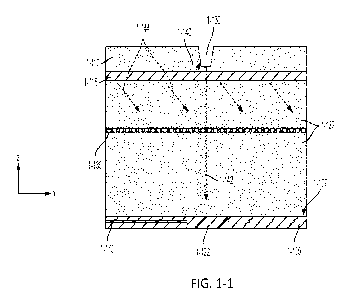
[0076] FIG. 1-1 is a simplified drawing that depicts some components that
may be included
in a pixel of, for example, a bio-optoelectronic chip. In a sample analysis
device, a pixel can
7
CA 03144003 2021-12-16
WO 2020/257445 PCT/US2020/038415
include a reaction chamber 1-130, an optical waveguide 1-115, an optical
nanostructure 1-135,
and a sensor 1-122 formed on a substrate 1-105. The waveguide 1-115 can
transport optical
energy to the pixel from a remote optical source and provide excitation
radiation to the reaction
chamber 1-130. Excitation radiation transported by waveguide 1-115 may be
coupled to reaction
chamber 1-130 via evanescent coupling in some embodiments. Arrow 1-140 depicts
coupling of
excitation radiation from waveguide 1-115 to reaction chamber 1-130. The
excitation radiation
may excite one or more analytes present in the reaction chamber 1-130. Emitted
radiation from
the analyte(s) can be detected by sensor 1-122. Arrow 1-142 depicts emission
radiation
propagating in the downward direction (although emission rays may be emitted
at other angles).
According to some embodiments, a signal, or lack thereof, from the sensor 1-
122 can provide
information about the presence or absence of an analyte in the reaction
chamber 1-130. In some
implementations, a signal from the sensor 1-122 can identify the type of
analyte present in the
reaction chamber.
[0077] For sample analysis, a sample containing one or more analytes may be
deposited over
the reaction chamber 1-130. For example, a sample may be disposed in a
reservoir or
microfluidic channel over the reaction chamber 1-130, such that the sample
comes into contact
with the reaction chamber. In some cases, a sample may be printed as a droplet
onto a treated
surface that includes the reaction chamber 1-130. During sample analysis, at
least one analyte
from a sample to be analyzed may enter into the reaction chamber 1-130. In
some
implementations, the analyte itself may fluoresce when excited by excitation
radiation 1-140
delivered from the waveguide 1-115. In some cases, the analyte may carry with
it one or more
linked fluorescent molecules. In yet other cases, the analyte may quench a
fluorophore already
present in the reaction chamber 1-130. When the fluorescing entity enters into
the reaction
chamber and is excited by excitation radiation, the fluorescing entity can
emit radiation, at a
different wavelength than the excitation radiation that is detected by the
sensor 1-122.
[0078] The inventors have recognized and appreciated that a portion of the
excitation
radiation traveling along waveguide 1-115 may radiate away from waveguide 1-
115, and in some
circumstances, may be received and detected by a sensor 1-122 (whether
directly from the
waveguide or upon reflection and/or scatter). Detection of excitation
radiation may interfere
with detection of emission radiation and decrease the signal-to-noise ratio.
This in turn can
negatively affect the device's ability to analyze or identify samples.
[0079] Radiation of excitation energy (indicated by arrows 1-144) away from
waveguide 1-
115 may arise due to scattering from the waveguide itself, which may result
from the roughness
of the waveguide's sidewalls or from the presence of other defects in the
waveguide, waveguide
interface with adjacent material, or in the adjacent material. Additionally,
or alternatively,
8
CA 03144003 2021-12-16
WO 2020/257445 PCT/US2020/038415
excitation energy may radiate away from the waveguide due to the fact that the
difference
between the refractive index of the waveguide's core and the refractive index
of the waveguide's
cladding is finite, giving rise to evanescent fields extending towards sensor
1-122.
[0080] The inventors have recognized and appreciated that detection of
excitation radiation
may be reduced, thus improving signal-to-noise ratio, by interposing an
optical rejecter such as
optical nanostructure 1-135 between waveguide 1-115 and sensor 1-122. The
optical
nanostructure may be configured to discriminate between signal and noise based
on a difference
in characteristic wavelength between the excitation radiation and the emission
radiation. The
optical nanostructure may be designed to reject (e.g., block or attenuate a
majority of) the
excitation radiation 1-144 while allowing emission radiation 1-142 to pass
through and reach
sensor 1-122. In some cases, a majority of emission radiation 1-142 incident
on the optical
nanostructure 1-135 and travelling toward the sensor 1-122 is transmitted
through the optical
nanostructure. In some embodiments, the optical nanostructure may include an
optical
nanostructure designed to exhibit at least one photonic bandgap, whereby
optical energy incident
on the optical nanostructure 1-135 and having a wavelength within a photonic
bandgap is
rejected.
[0081] The inventors have recognized and appreciated that photonic bandgap
optical rejecters
may be achieved by forming a periodic (or quasi-periodic) optical
nanostructure, with periodicity
in one, two, or three dimensions and structural variations in at least two
dimensions. In some
embodiments, the periodicity (or quasi-periodicity) may give rise to a
spectral band in which
propagation of light is prohibited (a photonic bandgap). The property is akin
to Bloch waves
having a certain wavelength that are prohibited inside a periodic solid-state
crystal. Within the
prohibited bandgap, radiation incident on the optical nanostructure interferes
destructively, and
as a result, is rejected. In some embodiments, an optical nanostructure may be
designed so that
the wavelength of the excitation radiation falls within the prohibited
photonic bandgap, while the
wavelength of the emission radiation falls outside the prohibited photonic
bandgap. As a result,
the emission radiation is transmitted and the excitations radiation is
reflected. In some
implementations, a majority of the emission radiation is transmitted and a
majority of the
excitation radiation is reflected. In some implementations, between 75% and
95% of the
emission radiation is transmitted and between 75% and 95% of the excitation
radiation is
reflected. In some implementations, between 85% and 99% of the emission
radiation is
transmitted and between 85% and 99% of the excitation radiation is reflected.
[0082] According to some embodiments, an opposite performance may be obtained,
whereby
an optical nanostructure is designed to exhibit an allowed photonic band
(rather than a prohibited
photonic bandgap). In these embodiments, wavelengths within the allowed
photonic band are
9
CA 03144003 2021-12-16
WO 2020/257445 PCT/US2020/038415
transmitted, while wavelengths outside the allowed band are rejected. In some
such
embodiments, an optical nanostructure may be designed so that the wavelength
of the excitation
radiation falls outside the allowed photonic band, while the wavelength of the
emission radiation
falls within the allowed photonic band. As a result, the emission radiation is
transmitted (at least
in part) and the excitations radiation is reflected (at least in part)
according to the amounts
described above in connection with the photonic bandgap optical nanostructure.
[0083] As noted above, optical nanostructures of the types described herein
are not limited to
use only in connection with integrated devices having the structure described
in FIG. 1-1. More
generally, embodiments of optical nanostructures described herein may be used
in applications in
which it is desired to reject one or more wavelengths or one or more ranges of
wavelengths, and
it is desired to permit transmission of one or more wavelengths or one or more
ranges of
wavelengths. Among other possible contexts, optical nanostructures described
herein may be
used in conjunction with optical communication systems, optical imaging
systems, Lidar
systems, etc.
[0084] FIG. 1-2 is a plot illustrating simulated spectral responses of an
example optical
nanostructure, according to some embodiments. In particular, FIG. 1-2 depicts
the reflection
coefficient (1-202), the transmission coefficient (1-204) and the absorption
coefficient (1-206)
associated with the example optical nanostructure as a function of wavelength.
The reflection
coefficient represents the ratio between the power of the reflected radiation
and the power of the
incident radiation. The transmission coefficient represents the ratio between
the power of the
transmitted radiation and the power of the incident radiation. The absorption
coefficient
represents the ratio between the absorbed power and the power of the incident
radiation. As
illustrated in FIG. 1-2, this optical nanostructure exhibits a prohibited
photonic bandgap (1-201)
between approximately 515 nm and approximately 550 nm. For wavelengths within
the
prohibited photonic bandgap 1-201, transmission coefficient 1-204 is less than
0.1, indicating
that less than 10% of the incident power passes through the optical
nanostructure. The remaining
power is either reflected or absorbed. In this case, 50% to 80% of the
incident power is reflected,
and the rest of the power is absorbed. Details of an example optical
nanostructure are provided
below.
[0085] For wavelengths outside the prohibited photonic bandgap 1-201,
larger amounts of
incident power can be transmitted through the optical nanostructure. At
wavelengths greater than
570 nm, for example, 50% or more of the incident power can be transmitted. At
wavelengths
greater than 600 nm, 90% of more of the incident power can be transmitted. In
some
embodiments, an optical nanostructure may be designed so that the wavelength
of the excitation
radiation falls within photonic bandgap 1-201 and the wavelength of the
emission radiation falls
CA 03144003 2021-12-16
WO 2020/257445 PCT/US2020/038415
outside photonic bandgap 1-201. In one specific example for this
nanostructure, the excitation
radiation may have a wavelength between 510 nm and 550 nm and the emission
wavelength can
be between 560 nm and 700 nm. Other values of excitation and emission
wavelengths are also
possible for optical nanostructures designed to have a photonic bandgap at a
different range of
wavelengths. Photonic bandgaps may have finite bandwidths. The bandwidth may
be, for
example, less than 150nm, less than 100nm, less than 50nm, or less than 30nm.
[0086] For the results plotted in FIG. 1-2, the example nanostructure was a
two-dimensional
periodic optical nanostructure (an example of which is depicted in FIG. 1-3D).
The
nanostructure was arranged as a cubic structure of silicon nitride posts
formed in a single layer of
silicon oxide material. The periodicity p3 of the posts was 250 nm and the
post width w3 was
140 nm. A thickness of the layer was 125 nm.
[0087] The spectral location of the photonic bandgap 1-201, and the values
of the coefficients
within and outside the photonic bandgap, may depend on different structural
features of the
nanostructure (e.g., periodicity, materials, post width or line width, post
shape, etc.), as will be
described further below. In some embodiments, the features of an optical
nanostructure may be
adjusted depending on the type of samples to be analyzed and/or the type of
excitation source
and emitters available. In some embodiments, the structural features may be
adjusted so that
between 25% and 15% inclusive of end values in some embodiments, between 15%
and 10%
inclusive of end values in some embodiments, between 10% and 5% inclusive of
end values in
some embodiments, and yet between 5% and 1% inclusive of end values in some
embodiments,
of the incident radiation within the photonic bandgap is transmitted through
the nanostructure. In
some cases, less than 1% of incident radiation within the photonic bandgap is
transmitted
through the nanostructure. In some embodiments, structural features may be
adjusted so that
between 50% and 75% inclusive of end values in some embodiments, between 75%
and 90%
inclusive of end values in some embodiments, between 90% and 95% inclusive of
end values in
some embodiments, and yet between 95% and 99% inclusive of end values in some
embodiments, of incident radiation outside the photonic bandgap is transmitted
through the
optical nanostructure. In some cases, more than 99% of the incident radiation
outside the
photonic bandgap is transmitted through the optical nanostructure.
[0088] The spectral response of FIG. 1-2 relates to an optical
nanostructure designed to
exhibit a prohibited photonic bandgap, whereby radiation with wavelengths
within the photonic
bandgap is rejected and radiation with wavelengths outside the photonic
bandgap is transmitted.
Alternatively, optical nanostructures may be designed to exhibit an allowed
photonic band,
whereby radiation with wavelengths within the allowed photonic band is
transmitted and
radiation with wavelengths outside the allowed photonic band is rejected. The
spectral response
11
CA 03144003 2021-12-16
WO 2020/257445 PCT/US2020/038415
of one such nanostructure (not illustrated in FIG. 1-2) may exhibit a high
transmission
coefficient (e.g., between 50% and 75% inclusive of end values in some
embodiments, between
75% and 90% inclusive of end values in some embodiments, between 90% and 95%
inclusive of
end values in some embodiments, and yet between 95% and 99% inclusive of end
values in some
embodiments) within the allowed photonic band, and a low transmission
coefficient (e.g.,
between 25% and 15% inclusive of end values in some embodiments, between 15%
and 10%
inclusive of end values in some embodiments, between 10% and 5% inclusive of
end values in
some embodiments, and yet between 5% and 1% inclusive of end values in some
embodiments)
outside the allowed photonic band. Such an optical nanostructures may be
designed so that the
wavelength of the excitation radiation falls outside the allowed photonic band
and the
wavelength of the emission radiation falls within the allowed photonic band.
[0089] Referring back to FIG. 1-1, reaction chamber 1-130 may be formed into a
transparent
or semitransparent layer 1-110. The reaction chamber may have a depth between
50 nm and
1 p.m, according to some embodiments. A minimum diameter of the reaction
chamber 1-130
may be between 50 nm and 300 nm in some embodiments. If the reaction chamber 1-
130 is
formed as a zero-mode waveguide, then the minimum diameter may be even less
than 50 nm in
some cases. If large analytes are to be analyzed, the minimum diameter may be
larger than 300
nm. The reaction chamber may be located above the optical waveguide 1-115 such
that a bottom
of the reaction chamber may be up to 500 nm above a top of the waveguide 1-
115. The
transparent or semitransparent layer 1-110 can be formed from an oxide or a
nitride, according to
some embodiments, so that excitation radiation from the optical waveguide 1-
115 and emission
radiation from the reaction chamber 1-130 will pass through the transparent or
semitransparent
layer 1-110 without being attenuated by more than 10%, for example.
[0090] In some implementations, there can be one or more additional
transparent or
semitransparent layers 1-137 formed on the substrate 1-105 and located between
the substrate
and the optical waveguide 1-115. These additional layers may be formed from an
oxide or a
nitride, and may be of the same type of material as the transparent or
semitransparent layer
1-110, in some implementations. The optical nanostructure 1-135 may be formed
within these
additional layers 1-137 between the waveguide 1-115 and sensor 1-122, for
example. A distance
from the bottom of the optical waveguide 1-115 to the sensor 1-122 can be
between 500 nm and
p.m.
[0091] In various embodiments, the substrate 1-105 may comprise a
semiconductor substrate,
such as silicon. However, other semiconductor materials may be used in some
embodiments.
The sensor 1-122 may comprise a semiconductor photodiode that is patterned and
formed on the
substrate 1-105. The sensor 1-122 may connect to other complementary metal-
oxide-
12
CA 03144003 2021-12-16
WO 2020/257445 PCT/US2020/038415
semiconductor (CMOS) circuitry on the substrate via interconnects 1-170.
[0092] An optical nanostructure 1-135 may be arranged to exhibit a
prohibited photonic
bandgap or an allowed photonic band. As described above, the spectral location
of the photonic
bandgap or allowed band may be chosen to reject excitation radiation and allow
emission
radiation to pass through the nanostructure to the sensor 1-122. In some
embodiments, an optical
nanostructure 1-135 is patterned to include structural variations and
periodicity in a plane parallel
to a surface (e.g., surface 1-107) of the substrate (the xy-plane in FIG. 1-
1). In some
embodiments, optical nanostructure 1-135 may have structural variations that
are periodic (or
quasi-periodic) in the xy-plane. The structural variations may be periodic (or
quasi-periodic) in
one dimension, such as along the x-axis or the y-axis, or in two dimensions,
such as along the x-
axis and the y-axis. In some embodiments, the structural variations may
involve two or more
materials of different refractive indexes.
[0093] An example of an optical nanostructure having periodicity in one
dimension and
structural variations in at least two dimensions is depicted in FIGs. 1-3A, in
accordance with
some embodiments. In an implemented one-dimensional structure, the bars may
extend a finite
distance in the y direction that is much greater than the periodicity or pitch
P1. In some
implementations, the extended distance in the y direction is much larger than
a region of interest
(e.g., diameter of reaction chamber 1-130, width of waveguide 1-115, or
diameter of sensor 1-
122). FIG. 1-3A illustrates an optical nanostructure that is periodic along
one axis (the x-axis in
this example) that is parallel or substantially parallel to surface 1-107 of
substrate 1-105. In this
example, optical nanostructure 1-135 includes two materials (1-302 and 1-304)
alternating along
the x-axis in a periodic fashion. Materials 1-302 and 1-304 have different
refractive indexes at
the wavelength of the emission radiation and/or have different refractive
indexes at the
wavelength of the excitation radiation. In some embodiments, an optical
nanostructure has no
missing or significantly different periodic component within the structural
variations. It should
be appreciated that, in some embodiments, more than two materials may be used
and may be
arranged in a periodic pattern (e.g., alternating of two materials or adding a
third material
periodically into the illustrated pattern).
[0094] Any suitable materials 1-302 and 1-304 may be used to form an
optical nanostructure
according to embodiments described herein. Example materials include, but are
not limited to,
one or both of dielectric and conductive materials. Examples of such
dielectric and conductive
materials include silicon (amorphous, nano-crystalline, micro-crystalline,
mono-crystalline or
poly-crystalline, doped or undoped), silicon nitride, silicon carbide, silicon
oxide and alloys or
mixtures thereof (including silicon-rich nitride and/or nitrogen-doped
silicon, among others), air,
polymer, aluminum, copper, titanium nitride, tungsten, titanium oxide,
germanium, tantalum, etc.
13
CA 03144003 2021-12-16
WO 2020/257445 PCT/US2020/038415
In one example, material 1-302 includes silicon and material 1-304 includes
silicon nitride. In
another example, material 1-302 includes silicon and material 1-304 includes
silicon oxide. In
another example, material 1-302 includes silicon and material 1-304 includes a
polymer. In
another example, material 1-302 includes silicon nitride and material 1-304
includes silicon
oxide. In another example, material 1-302 includes silicon nitride and
material 1-304 includes
air. Other combinations are also possible.
[0095] The inventors have discovered that certain materials may be used in the
design of an
optical nanostructure 1-135 to optimize performance, including silicon-rich
nitride materials
having specific n (refractive index) and k (extinction coefficient). Such
materials may be used as
filters in the design of an optical nanostructure, for example, or used to
form an optical
nanostructure 1-135 as described herein. Non-limiting examples of these
materials include
silicon-rich nitride materials. Characteristics of two examples of silicon-
rich nitride materials -
Silicon-rich Nitride I and Silicon-rich Nitride II - are respectively shown in
the graphs of FIGs.
6-1A and 6-1B. Shown in each graph are the n and k values of the material
versus wavelength.
[0096] In the illustrated example of FIG. 1-3A, an optical nanostructure 1-
135 includes a unit
cell that is repeated periodically along the x-axis. The periodicity (P1) with
which the unit cell is
repeated may be between 150 nm and 2 p.m in some embodiments, between 150 nm
and 1 p.m in
some embodiments, between 150 nm and 500 nm in some embodiments, between 150
nm and
400 nm in some embodiments, between 150 nm and 300 nm in some embodiments,
between 200
nm and 300 nm in some embodiments, between 230 nm and 270 nm in some
embodiments, or
between 240 nm and 260 nm in some embodiments. Other ranges are also possible.
The width
(W/) of a first material 1-302 along the x-axis may be between 50 nm and 1 p.m
in some
embodiments, between 50 nm and 500 nm in some embodiments, between 100 nm and
500 nm
in some embodiments, between 100 nm and 300 nm in some embodiments, between
150 nm and
300 nm in some embodiments, between 100 nm and 250 nm in some embodiments,
between 150
nm and 250 nm in some embodiments, between 100 nm and 150 nm in some
embodiments,
between 150 nm and 200 nm in some embodiments, between 130 nm and 150 nm in
some
embodiments, or between 130 nm and 140 nm in some embodiments. In some
embodiments,
periodicity P1 and width W/ may be selected so that the spectral response of
the resulting optical
nanostructure rejects excitation radiation and allows emission radiation to
pass through. For
example, P1 and W/ may be selected so that the characteristic wavelength of a
selected
excitation radiation falls within a prohibited photonic bandgap and the
characteristic wavelength
of a resulting emission radiation falls outside the prohibited photonic
bandgap, or so that the
wavelength of the emission radiation falls within an allowed photonic band and
the wavelength
of the excitation radiation falls outside the allowed photonic band.
14
CA 03144003 2021-12-16
WO 2020/257445 PCT/US2020/038415
[0097] Materials 1-302 and 1-304 may be formed into an optical
nanostructure in any suitable
way, such as using a fabrication process discussed below in connection with
FIGs. 4-1A through
4-1J. In some embodiments, materials 1-302 and 1-304 may be patterned through
one or more
lithographic steps, e.g., by using appropriately designed photomask(s) and
photolithography
processes. In some embodiments, material 1-302 includes a plurality of bars
extending along the
y-axis, as shown in the example of FIG. 1-3A, though different shapes and
orientations are also
possible.
[0098] In some embodiments, an optical nanostructure 1-135 may include
multiple material
layers arranged in a periodic or quasi-periodic fashion. Having multiple
layers, in some
embodiments, may improve the transmission and/or the reflection coefficient of
the optical
nanostructure. For example, having multiple layers may result in an increase
in the reflection
coefficient within a prohibited photonic bandgap and an increase in the
transmission coefficient
outside the prohibited photonic bandgap, or may result in an increase in the
transmission
coefficient within an allowed photonic band and an increase in the reflection
coefficient outside
the allowed photonic band.
[0099] FIG. 1-3B illustrates an example elevation view of a nanostructure
having multiple
material layers arranged in a periodic fashion, in accordance with some
embodiments. This
example illustrates an optical nanostructure having four layers that are
stacked in the z direction,
but any other suitable number of layers may be used. In a multilayer optical
nanostructure, each
layer may be formed at a different location along an axis perpendicular to
surface 1-107 of a
substrate 1-105 (e.g., along the z-axis). Each layer may include patterned
materials 1-302, 1-304
that is periodic in one dimension (as shown for example in FIG. 1-3A), or
periodic in two
dimensions (e.g., along the x-axis and the y-axis) in some cases. The optical
nanostructure of
FIG. 1-3B includes a first plurality of discrete regions (1-302) of first
material (e.g., dielectric
material or conductive material), and a second plurality of discrete regions
(1-304) of second
material having a different index of refraction (dielectric material,
conductive material, or air).
[0100] In some embodiments, the discrete regions of one layer are staggered
with respect to
the discrete regions of another layer. In the example optical nanostructure of
FIG. 1-3B, for
example, each of the first and third layers is staggered along the x-axis with
respect to the second
and fourth layers.
[0101] Each layer of a multilayer optical nanostructure may have a height
(H1) or thickness
that is between 50nm and 1 p.m in some embodiments, between 50 nm and 500 nm
in some
embodiments, between 100 nm and 500 nm in some embodiments, between 100 nm and
300 nm
in some embodiments, between 150 nm and 300 nm in some embodiments, between
100 nm and
250 nm in some embodiments, between 150 nm and 250 nm in some embodiments,
between 100
CA 03144003 2021-12-16
WO 2020/257445 PCT/US2020/038415
nm and 150 nm in some embodiments, between 150 nm and 200 nm in some
embodiments,
between 120 nm and 150 nm in some embodiments, between 120 nm and 140 nm in
some
embodiments, between 120 nm and 130 nm in some embodiments, or between 130 nm
and 140
nm in some embodiments. Other ranges are also possible. Different layers may
have different
heights. Alternatively, all the layers may have essentially the same height.
[0102] In some embodiments, an optical nanostructure may have structural
variations that are
periodic or quasi-periodic in two dimensions within a plane. Examples of
optical nanostructures
having structural variations in two dimensions within a plane are depicted in
FIGs. 1-3C and 1-
3D. In the example of FIG. 1-3C, columns of a second material 1-314 are
separated from each
other by regions of a first material 1-312. The first and second materials 1-
312, 1-314 may be
any of the materials described above for materials 1-302, 1-304. In the
example of FIG. 1-3C,
the second material 1-314 may have a lower value of index of refraction than
the first material 1-
312. In the example of FIG. 1-3D, columns of a first material 1-322 are
separated from each
other by regions of a second material 1-324. The first and second materials 1-
322, 1-324 may be
any of the materials described above for materials 1-302, 1-304. In the
example of FIG. 1-3D,
the second material 1-324 may have a higher value of index of refraction than
the first material
1-322.
[0103] For the examples depicted in FIG. 1-3C and FIG. 1-3D, the
periodicities along the x-
axis (P2 and P3) may have a value in any of the ranges described above in
connection with FIG.
1-3A. Similarly, the periodicities along the y-axis may have a value in any of
the ranges
described above in connection with FIG. 1-3A. A feature formed from one
material within a
unit cell of a planar, two-dimensional optical nanostructure may have any
suitable shape, such as
square, rectangular, polygonal, triangular, circular, or irregular. Widths (W2
and W3) of
structural features along the x-axis may have a value in any of the ranges
described above in
connection with FIG. 1-3A. Similarly, widths of structural features along the
y-axis may have a
value in any of the ranges described above in connection with FIG. 1-3A. In
some
embodiments, multiple layers of a planar, two-dimensional optical
nanostructure, such as those
shown in FIG. 1-3C or FIG. 1-3D, may be formed in a stack along the z-axis.
The layers may
be staggered similar to the arrangement of FIG. 1-3B. The height (H3) of each
layer may have a
value in any of the ranges described above in connection with FIG. 1-3B.
[0104] Compared to optical nanostructures periodic in one dimension, those
periodic in two or
three dimensions provide additional design parameters. As a result, optical
nanostructures
periodic in two or three dimensions provide greater flexibility to engineer a
desired spectral
response. In some embodiments, for example, optical nanostructures periodic in
two or three
dimensions have flatter spectral responses within the photonic bandgap or
allowed photonic band
16
CA 03144003 2021-12-16
WO 2020/257445 PCT/US2020/038415
and/or steeper roll-offs at edges of the photonic bandgap or allowed photonic
band. Steeper roll-
offs can lead to a greater differential between the transmission coefficient
and the reflection
coefficient excitation and emission wavelengths that are near an edge of the
photonic bandgap or
allowed band.
[0105] The examples described in connection with FIGs. 1-3A, 1-3B, 1-3C and 1-
3D exhibit
periodicities in one or two dimensions. Additionally, or alternatively, quasi-
periodic optical
nanostructures may be used to achieve a spectral response characterized by
prohibited photonic
bandgap or allowed photonic band. Quasi-periodic optical nanostructures of the
types described
therein may include two or more alternating building blocks, in accordance
with some
embodiments. Examples of quasi-periodic optical nanostructures include one
dimensional
photonic structures based on the Fibonacci sequence (shown in FIG. 1-3E), two
dimensional
photonic structures based on the Penrose structure (shown in FIG. 1-3F), three
dimensional
photonic structures with icosahedral quasi-crystalline structures, one, two or
three dimensional
photonic structures based on the Thue-Morse sequence, one, two or three
dimensional photonic
structures based on the period-doubling sequence, one, two or three
dimensional photonic
structures based on the Rudin-Shapiro sequence, one, two or three dimensional
photonic
structures based on the Cantor sequence, and others. Some such structures may
give rise to
spectral responses with photonic bandgaps or allowed bands even if they do not
have
translational symmetry. Quasi-periodic structures of the types described
herein may be
deterministically aperiodic.
[0106] Referring back to FIG. 1-1, the presence of an optical nanostructure
between
waveguide 1-115 and sensor 1-122 may result in the rejection of excitation
radiation 1-144 while
allowing transmission of emission energy 1-142. The excitation radiation 1-144
may come
directly from waveguide 1-115 and/or be scattered from other surfaces of the
device. The
inventors have recognized and appreciated that an optical nanostructure of the
present
embodiments can be more effective at reducing transmission of excitation
radiation 1-144 from a
wide range of angles than, for example, a multilayer dielectric interference
filter.
[0107] FIGs. 1-4A and 1-4B depict example electric field patterns
calculated for an integrated
device having example structure similar to that depicted in FIG. 1-1. However,
a microdisk is
included in the simulation and is located between the waveguide 1-115 and the
optical
nanostructure 1-135. The microdisk is described further below and helps
concentrate emission
radiation onto the sensor 1-122. For this simulation, the waveguide 1-115 and
optical
nanostructure comprise silicon nitride surrounded by silicon oxide. The
optical nanostructure is
formed as a single-layer, planar, two-dimensional nanostructure having a cubic
crystal like that
shown in FIG. 1-3D. The first material 1-322 is formed from silicon nitride
and the second
17
CA 03144003 2021-12-16
WO 2020/257445 PCT/US2020/038415
material 1-324 is formed from silicon oxide. The pitch P3 is 260nm, the width
W3 is 160 nm,
and the thickness of the layer H3 is 125 nm for this example.
[0108] For this example simulation the excitation radiation has a
characteristic wavelength
(XXexcitation) of 532 nm and at the emission radiation has a characteristic
wavelength (Xkemission)
of 572 nm. Other optical nanostructure parameters (periodicity, width,
thickness, etc.) and/or
other wavelengths (including for example excitation wavelengths in the 500 nm-
540 nm range to
produce emission wavelengths in the 620 nm-650 nm range) may be used in other
embodiments.
The electric fields patterns were computed with software that solves Maxwell's
equations (e.g.,
using a finite-difference time-domain analysis) within the simulation domain
with the following
initial conditions for the excitation and emission radiation: 1) radiation at
_),=¨), excitation is coupled
into the single-mode waveguide 1-115 from an external source, and 2) radiation
at _),=_), emission is
generated in the reaction chamber 1-130.
[0109] As illustrated in FIG. 1-4A for k==-,-xcitation, a significant
portion of the electric field is
confined within waveguide 1-115 which delivers the excitation radiation to the
reaction chamber
1-130. However, an appreciable amount of the electric field for the excitation
radiation extends
below the waveguide 1-115 due to an evanescent field associated with the
waveguide and scatter
from walls of the waveguide and other structure within the pixel that includes
the reaction
chamber. The optical nanostructure 1-135 can reflect most of the excitation
electric field back
toward the waveguide. Absent optical nanostructure 1-135, the electric field
may reach sensor 1-
122 and contribute to background noise. This result would be undesirable as it
may reduce the
signal-to-noise ratio of the detection system. Use of an optical nanostructure
between waveguide
1-115 and sensor 1-122 leads to a substantial reduction in the magnitude of
the electric field in
the region adjacent to sensor 1-122. As a result, the amount of detected
excitation energy is
reduced significantly.
[0110] As illustrated in FIG. 1-4B, emission radiation at k=¨),-mission
proceeding from the
reaction chamber 1-130 toward the sensor is mostly transmitted through the
optical nanostructure
1-135 and can travel to the sensor 1-122. As noted above, the microdisk 145
helps concentrate
or condense emission radiation onto the sensor 1-122.
[0111] The inventors have further recognized that excitation radiation may
strike optical
nanostructure 1-135 at different incident angles in some circumstances. This
may be due, among
other possible reasons, as a result of the excitation radiation being
reflected multiple times and
scattering off structure within the pixel before striking the optical
nanostructure. Recognizing
this problem, the inventors have appreciated that an advantageous
characteristic of an optical
nanostructure of the present embodiments is a capability to reject radiation
over a wider range of
incident angles than multilayer interference filters, for example.
18
CA 03144003 2021-12-16
WO 2020/257445 PCT/US2020/038415
[0112] Compared to other types of optical rejecters, the optical
nanostructures of the types
described herein provide optical rejection across wide ranges of incident
angles. For a single
layer optical nanostructure, this behavior is due to the presence of periodic
or quasi-periodic
structural variations (in one or two dimensions) in the xy-plane. FIG. 1-5 is
a plot illustrating a
rejection ratio associated with two different optical structures at
wavelengths of interest plotted
as a function of angle of incidence (horizontal axis). The rejection ratio is
a ratio of an amount of
emission radiation at a characteristic emission wavelength (572 nm in this
example) transmitted
through the optical structure divided by an amount of excitation radiation at
a characteristic
excitation wavelength (532 nm in this example) that is transmitted through the
optical structure.
A same amount of power is incident on the optical structure for the emission
radiation and
excitation radiation. The angle of incidence is measured with respect to a
normal to the planar
surface of the optical structure.
[0113] A first rejection ratio curve 1-501 is plotted for a multi-layer
interference filter having
23 layers (though any other number of layers may be used, such as between 10
and 50 layers,
between 10 and 40 layers, between 20 and 50 layers, or between 20 and 40
layers, among others)
with alternating refractive indexes along the z-axis. This optical structure
does not exhibit
structural variations in the xy-plane. Thus, in each xy-plane, the refractive
index is uniform. The
rejection ratio for this optical structure is relatively high below 20 , but
drops significantly for
incident angles greater than 20 . This drop means that an appreciable amount
of excitation
radiation striking the optical structure with angles greater than about 22 is
transmitted through
the optical structure and can contribute to background signal at the sensor 1-
122.
[0114] A second rejection ratio curve 1-502 is plotted for an example
single-layer optical
nanostructure of the present embodiments having in-plane structural
variations. The example
optical nanostructure has a cubic lattice with essentially square columns of
silicon nitride
embedded in silicon oxide. The columns have a width of 140 nm and the
periodicity in both the
x and y directions is 250 nm. A thickness of the layer is 125 nm. As
illustrated in FIG. 1-5, the
rejection ratio is greater than about 10 for all angles below 45 . Hence, this
optical nanostructure
can provide better rejection of excitation radiation over a wider range of
incident angles than
multilayer interference filters.
[0115] Another example of optical structures that may be included at a
pixel of an integrated
device is shown in FIG. 2-1. According to some implementations, one or more
iris layers 2-110
may be formed above the sensor 1-122. An iris layer 2-110 may include an
opening or hole 2-
112 through a light-reducing material. The light-reducing material may
comprise a metal,
polymer, semiconductor, or any material that rejects (e.g., absorbs and/or
reflects) a majority of
excitation radiation incident on the iris layer 2-110. The light-reducing
material may also reject
19
CA 03144003 2021-12-16
WO 2020/257445 PCT/US2020/038415
emission radiation in some cases. The hole 2-112 can allow emission from the
reaction chamber
1-130 to pass through the iris layer 2-110 and reach sensor 1-122, while the
light-reducing
material blocks or attenuates radiation from other directions (e.g., from
adjacent pixels or from
scattered excitation radiation). For example, an iris layer 2-110 can block or
attenuate scattered
excitation radiation at wide angles of incidence from striking the sensor 1-
122 and contributing
to background noise. In some embodiments, an iris layer 2-110 may be formed
from a
conductive material and provide a potential reference plane or grounding plane
for circuitry
formed on or above the substrate 1-105. In some embodiments, an iris layer 2-
110 may be
formed from a dielectric material. The hole 2-112 in the iris layer may be
shaped in any suitable
way, such as a square, rectangle, disk, ellipse, polygon, etc.
[0116] In the example of FIG. 2-1, two iris layers 2-110 are included. One
iris layer is
disposed between waveguide 1-115 and optical nanostructure 1-135. Another iris
layer is
disposed between optical nanostructure 1-135 and sensor 1-122. It should be
appreciated,
however, that any other suitable number of iris layers and locations may be
used. In some cases,
a single iris layer may be used and may be located between the reaction
chamber 1-130 and
optical nanostructure 1-135 or between the optical nanostructure 1-135 and
sensor 1-122.
[0117] In some embodiments, a condensing optical element 2-160 may be used to
concentrate
emission radiation emitted from the reaction chamber onto the sensor. In the
example of FIG. 2-
1, a condensing optical element 2-160 is located between the reaction chamber
1-130 and the
optical nanostructure 1-135, though other placements are also possible.
According to some
embodiments, a condensing optical element 2-160 may be made of one or more
materials
transparent at the wavelength of the emission radiation, and with a refractive
index different
(e.g., greater) than the refractive index of the material surrounding the
condensing optical
element 2-160. In this way, the condensing optical element 2-160 can provide
some focusing of
emission radiation from the reaction chamber 1-130. In some embodiments, an
optical element
2-160 may be shaped as a disk (e.g., a microdisk), thereby providing
rotational symmetry.
Optical element 2-160 may be positioned such that the center of the disk is
aligned, along the z-
axis, with the center of the reaction chamber 1-130. In some embodiments,
reaction chamber 1-
130, optical element 2-160, irises 2-112 and sensor 1-122 may be aligned to
one another along
the z-axis.
[0118] According to some embodiments, devices of the types described herein
may fabricated
by successive steps of material deposition and patterning to build up the
multiple levels in a chip
for an integrated device. In some implementations, a chip for an integrated
device may be
obtained by bonding two substrates or wafers to one another. For example, an
integrated device
(for which example structure at a pixel is depicted in FIG. 2-1) may be formed
from a bio-optical
CA 03144003 2021-12-16
WO 2020/257445 PCT/US2020/038415
substrate 1-100 that can be aligned and bonded to a CMOS substrate 1-101. An
example bio-
optical substrate 1-100 can include several pixels, each pixel having a
reaction chamber 1-130, a
waveguide 1-115, an optical nanostructure 1-135, and optionally, one or more
iris layers 2-110
and one or more optical elements 2-160. An example CMOS substrate 1-101 can
include several
corresponding pixels having sensors 1-122 (e.g., one per pixel) and circuitry
for processing
signals generated by the sensors. Layers 2-202 represent conductor layers or
semiconductor
layers that may be used for routing and/or processing the signals.
[0119] The effect of a pair of iris layers 2-110 and a condensing optical
element 2-160 is
depicted in FIG. 2-2, in accordance with some embodiments. As illustrated,
rays emitted
substantially parallel to the z-axis pass straight through the openings in the
iris layers. Rays
emitted with angles deviating substantially from the z-axis are rejected by
one of the iris layers 2-
110. Rays emitted with smaller angles are focused by the optical element 2-
160. As a result,
radiation emitted from reaction chamber 1-130 is concentrated onto sensor 1-
122, thus increasing
the signal-to-noise ratio.
[0120] Another example of a structure that may be included at a pixel of an
integrated device
is shown in FIG. 2-3. According to some implementations, one or more light-
reducing layers 2-
150 may be formed over layer 1-110, into which a reaction chamber 1-130 may be
formed. The
light-reducing layers 2-150 may be formed from one or more metal layers. In
some cases, the
light-reducing layers 2-150 may include a semiconductor and/or oxide layer.
The light-reducing
layers 2-150 may reduce or prevent excitation radiation from the optical
waveguide 1-115 from
travelling into a sample above the reaction chamber 1-130 and exciting
fluorophores within the
sample. Additionally, the light-reducing layers 2-150 can prevent external
radiation from above
the reaction chamber to pass through to the sensor 1-122. Emission from
outside the reaction
chamber can contribute to unwanted background radiation and signal noise.
Light-reducing
layers 2-150 may be used in conjunction with any of the embodiments described
herein.
[0121] Example structure 3-100 for a disposable chip is shown in FIG. 3,
according to some
embodiments. The disposable chip structure 3-100 may include a bio-
optoelectronic chip 3-110
having a semiconductor substrate 3-105 and including a plurality of pixels 3-
140 formed on the
substrate. Each pixel 3-140 may have a structure and an embodiment of an
optical nanostructure
as described above in connection with FIG. 1-1 through FIG. 2-3. In some
embodiments, there
may be rows (or columns) of waveguides 3-115 that provide excitation radiation
to rows (or
columns) of pixels 3-140. Waveguide 1-115 of FIG. 1-1 may serve as any one of
such
waveguides in some implementations. Excitation radiation may be coupled into
the waveguides,
for example, through an optical port 3-150. In some embodiments, a grating
coupler may be
formed on the surface of the bio-optoelectronic chip 3-110 to couple
excitation radiation from a
21
CA 03144003 2021-12-16
WO 2020/257445 PCT/US2020/038415
focused beam into one or more receiving waveguides that connect to the
plurality of waveguides
3-115.
[0122] The disposable chip structure 3-100 may further include walls 3-120
that are formed
around a pixel region on the chip 3-110. The walls 3-120 may be part of a
plastic or ceramic
casing that supports the chip. The walls 3-120 may form at least one reservoir
3-130 into which
at least one sample may be placed and come into direct contact with reaction
chambers 1-130 on
the surface of the bio-optoelectronic chip 3-110. The walls 3-120 may prevent
the sample in the
reservoir 3-130 from flowing into a region containing the optical port 3-150
and grating coupler,
for example. In some embodiments, the disposable chip structure 3-100 may
further include
electrical contacts on an exterior surface of the disposable chip and
interconnects within the
package, so that electrical connections can be made between circuitry on the
bio-optoelectronic
chip 3-110 and circuitry in an instrument into which the chip is mounted.
[0123] As noted above, an optical nanostructure 1-135 is not limited only
to a disposable chip
3-100 as depicted in FIG. 3. Example embodiments of an optical nanostructure 1-
135 may be
included in other chips, such as imaging chips having photosensor arrays. Such
imaging chips
may be used in cameras, video cameras, smart phones, and optical sensing
arrays.
[0124] II. Methods for fabricating optical nanostructures
[0125] FIGs. 4-1A through 4-1J illustrate, example structure associated
with a method for
fabricating an optical nanostructure (such as any one of the optical
nanostructures described
above). In the process step depicted in FIG. 4-1A, a substrate 4-100 is
provided or obtained
upon which lithography steps may be performed. Substrate 4-100 may include
some structure
already formed on the substrate 4-100. For example, a substrate 4-100 may
include part of the
structure shown in FIG. 1-1 or FIG. 2-1 below the optical nanostructure 1-135.
In some
embodiments, substrate 4-100 may comprise a bulk semiconductor substrate,
though other types
of bulk substrates may be used in some implementations.
[0126] According to some embodiments, a first material layer 4-102 may be
deposited or
grown on substrate 4-100, as depicted in FIG. 4-1B. The first material layer 4-
102 may be
deposited, for example, by physical vapor deposition (PVD), plasma-enhanced
chemical vapor
deposition (PECVD), high-density plasma (HDP) PECVD, or sputtering. The first
material layer
4-102 may include amorphous silicon, silicon nitride, titanium nitride,
titanium oxide, among
other possible materials described above for an optical nanostructure 1-135,
silicon-rich nitride
materials having specific n (refractive index) and k (extinction coefficient)
values such as
Silicon-rich Nitride I and Silicon-rich Nitride II. Subsequently, a
photoresist layer 4-104 can be
deposited on the first material layer 4-102 and patterned using a
photolithographic exposure and
22
CA 03144003 2021-12-16
WO 2020/257445 PCT/US2020/038415
develop process, as depicted in FIG. 4-1C. Using the patterned photoresist
layer 4-104 as an
etch mask, the first material layer 4-102 can be etched in regions where the
photoresist has been
removed to form voids in the first material layer 4-102, as depicted in FIG. 4-
1D. The remaining
photoresist may be removed from the substrate in a cleaning step. The
resulting structure of the
etched first material layer 4-102 may comprise a plurality of material regions
4-106, which may
be arranged, for example, in accordance to one of the single-layer structures
described above in
connection with FIGs. 1-3A through FIG. 1-3F. Material regions 4-106 may form
columns of
an optical nanostructure 1-135, for example.
[0127] In some implementations, a second material layer 4-108 (having a
different refractive
index than the first material layer) can be deposited on the material regions
4-106, as depicted in
FIG. 4-1E. The second material layer 4-108 may be deposited by any suitable
deposition
process, such as PVD, PECVD, HDP PECVD, or sputtering. The second material
layer 4-108
may comprise silicon oxide, silicon nitride, titanium nitride, titanium oxide,
among other
possible materials described above for an optical nanostructure 1-135, silicon-
rich nitride
materials having specific n (refractive index) and k (extinction coefficient)
values such as
Silicon-rich Nitride I and Silicon-rich Nitride II. In some cases, the second
material layer 4-108
fills the regions between material regions 4-106. According to some
implementations, the
second material layer 4-108 may be planarized, for example via chemical-
mechanical polishing
(CMP), resulting in a planar surface as depicted in FIG. 4-1F. However, in
some cases one or
more layers may be deposited on the second material layer 4-108 without
performing a
planarization step of the second material layer 4-108. In some embodiments,
the structure
depicted in FIG. 4-1F may form an optical nanostructure 1-135, and be
arranged, for example, in
accordance to one of the single-layer structures described above in connection
with FIGs. 1-3A
through FIG. 1-3F.
[0128] Optionally, one or more additional layers may be added to the
optical nanostructure,
leading for example to the arrangement of FIG. 1-3B. FIGs. 4-1G through FIG. 4-
1J depict
structures associated with steps for forming a second nanostructure layer, in
accordance with
some embodiments. Additional layers may be formed using similar steps. In some
implementations, a third material layer 4-110 can be deposited or grown on the
second material
layer 4-108, as depicted in FIG. 4-1G. The third material layer 4-110 may be
deposited, for
example, by PVD, PECVD, HDP PECVD, or sputtering. The third material layer 4-
110 may
include amorphous silicon, silicon nitride, titanium nitride, titanium oxide,
among other possible
materials described above for an optical nanostructure 1-135, silicon-rich
nitride materials having
specific n (refractive index) and k (extinction coefficient) values such as
Silicon-rich Nitride I
and Silicon-rich Nitride II. In some implementations, the third material layer
4-110 may be the
23
CA 03144003 2021-12-16
WO 2020/257445 PCT/US2020/038415
same material as the first material layer 4-102. A photoresist layer 4-112 can
be deposited on the
third material layer 4-110 and patterned using a photolithographic exposure
and develop process,
according to some embodiments. Using the patterned photoresist layer 4-112 as
an etch mask,
the third material layer 4-110 can be etched in regions where the photoresist
has been removed,
as depicted in FIG. 4-1H. Residual photoresist can be removed from the
substrate after etching.
The resulting structure includes a plurality of material regions 4-114.
[0129] Subsequently, a fourth material layer 4-116 can be deposited on the
material regions 4-
114, for example via PVD, PECVD, HDP PECVD, or sputtering. In some cases, the
fourth
material layer 4-116 fills the regions between the material regions 4-114, as
depicted in FIG. 4-
11. According to some embodiments, the fourth material layer 4-116 may be made
of a material
having a refractive index different from the refractive index of the third
material layer 4-110.
The fourth material layer 4-116 may include silicon oxide, silicon nitride,
titanium nitride,
titanium oxide, among other possible materials described above for an optical
nanostructure 1-
135, silicon-rich nitride materials having specific n (refractive index) and k
(extinction
coefficient) values such as Silicon-rich Nitride I and Silicon-rich Nitride
II. In some cases, the
fourth material layer 4-116 may be a same material as the second material
layer 4-108.
According to some implementations, the fourth material layer 4-116 can be
planarized, for
example using a CMP process step, resulting in a planar surface as depicted in
FIG. 4-1J. In
other implementations, one or more layers may be deposited on the fourth
material layer 4-116
without planarizing the fourth material layer.
[0130] Additional examples of structures associated with another example
method for
fabricating an optical nanostructure are depicted in FIGs. 4-2A through FIG. 4-
2J. This
fabrication method is similar in some respects to the fabrication method of
FIGs. 4-1A through
FIG. 4-1J. Unlike the fabrication method of FIGs. 4-1A through FIG. 4-1J,
however, dual
mask layers 4-104/4-103 and 4-112/4-111 are used as etch masks for the
formation of the
material regions. Substrate 4-100 and layers 4-102, 4-104, 4-106, 4-108, 4-
110, 4-112, 4-114
and 4-116 may have the same characteristics as those described in connection
with FIGs. 4-1A
through FIG. 4-1J. Dual mask layers (sometimes referred to as a bilayer
resist) can provide
improved etch selectivity or improved patterning fidelity compared to a single
photoresist layer
in some cases. In some embodiments, one of the mask layers (e.g., 4-103, 4-
111) may comprise
a so-called "hard mask" formed from a metal, oxide, nitride, or semiconductor,
for example.
[0131] An example method of forming an optical nanostructure 1-135 may
comprise
obtaining a substrate 4-100 as depicted in FIG. 4-2A. As noted above in
connection with FIG.
4-1A, the substrate may include patterned structure. A first material layer 4-
102 may be
deposited or grown on substrate 4-100, as described above. Additionally, a
first resist layer 4-
24
CA 03144003 2021-12-16
WO 2020/257445 PCT/US2020/038415
103 can be deposited on the first material layer 4-102, as depicted in FIG. 4-
2B. The first resist
layer 4-103 may be a hard material rather than a polymer. For example, the
first resist layer 4-
103 may comprise silicon oxide, silicon nitride, or tantalum, among other
possible materials,
silicon-rich nitride materials having specific n (refractive index) and k
(extinction coefficient)
values such as Silicon-rich Nitride I and Silicon-rich Nitride II. According
to one example, the
first material layer 4-102 may be silicon nitride and the first resist layer 4-
103 may be silicon
oxide, though other material combinations can be used. A photoresist layer 4-
104 (a second
resist layer) may then be deposited on the first resist layer 4-103 and
patterned using a
photolithographic exposure and develop process to produce the structure
depicted in FIG. 4-2C.
Using the patterned photoresist layer 4-104 as a first etch mask, the first
resist layer 4-103 can be
etched in regions where the photoresist has been removed to transfer the
pattern from the
photoresist to the first resist layer 4-103, as depicted in FIG. 4-2D. During
and/or after this
etching step, the photoresist layer 4-104 may be removed.
[0132] Using the first resist layer 4-103 as an etch mask, the first
material layer 4-102 can be
etched in regions where the first resist layer 4-103 has been removed to form
voids in the first
material layer 4-102. The etching process leaves material regions 4-106 as
depicted in FIG. 4-
2E. In some cases, the remaining first resist layer 4-103 may be removed from
the substrate. In
other cases, the remaining first resist layer may be left on the material
regions 4-106 as illustrated
in FIG. 4-2E. In some cases, the first resist layer may be much thinner than
the first material
layer 4-102 and second material layer 4-108 and not appreciably affect
performance of the
optical nanostructure 4-135. In some implementations, the first resist layer 4-
103 may be a same
material as the second material layer 4-108. After etching to form material
regions 4-106, a
second material layer 4-108 can be deposited on the material regions 4-106, as
depicted in FIG.
4-2F. The second material layer may fill regions between the material regions
4-106. In some
cases, the second material layer 4-108 may be planarized, for example via CMP.
The structure
of FIG. 4-2F may form a single-layer optical nanostructure 1-135 described
above in connection
with FIGs. 1-3A through FIG. 1-3F.
[0133] Optionally, one or more additional layers may be added to the
optical nanostructure,
leading for example to the arrangement of FIG. 1-3B. FIGs. 4-2G through FIG. 4-
2J depict
structures associated with steps for forming a second nanostructure layer, in
accordance with
some embodiments. Additional layers may be formed using similar steps. For
example, a third
material layer 4-110 can be deposited or grown on the second material layer 4-
108, as depicted in
FIG. 4-2G. Subsequently, a first resist layer 4-111 can be deposited on the
third material layer
4-110, and a photoresist layer 4-112 can be deposited on the first resist
layer 4-111. The
photoresist layer can be patterned using a photolithographic exposure and
develop process. The
CA 03144003 2021-12-16
WO 2020/257445 PCT/US2020/038415
photoresist layer 4-112 can provide an etch mask to etch the first resist
layer 4-111 in regions
where the photoresist has been removed, and the first resist layer can provide
an etch mask to
etch the third material layer 4-110, as described above and depicted in FIG. 4-
2H. Residual
photoresist 4-112 may be removed during or after the etching of the third
material layer 4-110.
Etching of the third material layer 4-110 forms material regions 4-114. A
fourth material layer
4-116 can be deposited on the material regions 4-114 and may fill spaces
between the material
regions 4-114, as depicted in FIG. 4-21. According to some embodiments, the
fourth material
layer 4-116 may be planarized, as depicted in FIG. 4-2J.
[0134] The illustrations in FIG. 4-1H and FIG. 4-2H indicate that the
second material regions
4-114 are formed above the first material regions 4-106, such that bottoms of
the second material
regions 4-114 are spaced vertically away from tops of the first material
regions 4-106 with a
uniform layer of the second material layer 4-108 between these bottoms and
tops. However,
there may not be a space between these bottoms and tops in some
implementations. For
example, a planarization step of the second material layer may remove most or
all of the second
material layer 4-108 that is above the tops of the first material regions 4-
106, so that the bottoms
of the second material regions 4-114 are at essentially a same height as tops
of the first material
regions 4-106.
[0135] III. Example Bioanalytic Application
[0136] An example bioanalytic application is described in which an
integrated semiconductor
can be used to improve detection of radiation emitted from reaction chambers
on a disposable
chip that is used in an advanced analytical instrument. When mounted in a
receptacle of the
instrument, the disposable chip can be in optical and electronic communication
with optical and
electronic apparatus within the advanced analytic instrument. The instrument
may include
hardware for an external interface, so that data from the chip can be
communicated to an external
network. In embodiments, the term "optical" may refer to ultra-violet,
visible, near-infrared, and
short-wavelength infrared spectral bands. Although various types of analyses
can be performed
on various samples, the following explanation describes genetic sequencing.
However, the
invention is not limited to instruments configured for genetic sequencing.
[0137] In overview and referring to FIG. 5-1A, a portable, advanced
analytic instrument 5-
100 can comprise one or more pulsed optical sources 5-108 mounted as a
replaceable module
within, or otherwise coupled to, the instrument 5-100. The portable analytic
instrument 5-100
can include an optical coupling system 5-115 and an analytic system 5-160. The
optical coupling
system 5-115 can include some combination of optical components (which may
include, for
example, none, one from among, or more than one component from among the
following
26
CA 03144003 2021-12-16
WO 2020/257445 PCT/US2020/038415
components: lens, mirror, optical filter, attenuator, beam-steering component,
beam shaping
component) and be configured to operate on and/or couple output optical pulses
5-122 from the
pulsed optical source 5-108 to the analytic system 5-160. The analytic system
5-160 can include
a plurality of components that are arranged to direct the optical pulses to at
least one reaction
chamber for sample analysis, receive one or more optical signals (e.g.,
fluorescence,
backscattered radiation) from the at least one reaction chamber, and produce
one or more
electrical signals representative of the received optical signals. In some
embodiments, the
analytic system 5-160 can include one or more photodetectors and may also
include signal-
proces sing electronics (e.g., one or more microcontrollers, one or more field-
programmable gate
arrays, one or more microprocessors, one or more digital signal processors,
logic gates, etc.)
configured to process the electrical signals from the photodetectors. The
analytic system 5-160
can also include data transmission hardware configured to transmit and receive
data to and from
external devices (e.g., one or more external devices on a network to which the
instrument 5-100
can connect via one or more data communications links). In some embodiments,
the analytic
system 5-160 can be configured to receive a bio-optoelectronic chip 5-140,
which holds one or
more samples to be analyzed.
[0138] FIG. 5-1B depicts a further detailed example of a portable
analytical instrument 5-100
that includes a compact pulsed optical source 5-108. In this example, the
pulsed optical source
5-108 comprises a compact, passively mode-locked laser module 5-110. A
passively mode-
locked laser can produce optical pulses autonomously, without the application
of an external
pulsed signal. In some implementations, the module can be mounted to an
instrument chassis or
frame 5-102, and may be located inside an outer casing of the instrument.
According to some
embodiments, a pulsed optical source 5-108 can include additional components
that can be used
to operate the optical source and operate on an output beam from the optical
source 5-108. A
mode-locked laser 5-110 may comprise an element (e.g., saturable absorber,
acousto-optic
modulator, Kerr lens) in a laser cavity, or coupled to the laser cavity, that
induces phase locking
of the laser's longitudinal frequency modes. The laser cavity can be defined
in part by cavity end
mirrors 5-111, 5-119. Such locking of the frequency modes results in pulsed
operation of the
laser (e.g., an intracavity pulse 5-120 bounces back-and-forth between the
cavity end mirrors)
and produces a stream of output optical pulses 5-122 from one end mirror 5-111
which is
partially transmitting.
[0139] In some cases, the analytic instrument 5-100 is configured to
receive a removable,
packaged, bio-optoelectronic or optoelectronic chip 5-140 (also referred to as
a "disposable
chip"). The disposable chip can include a bio-optoelectronic chip 3-110, as
depicted in FIG. 4
for example, that comprises a plurality of reaction chambers, integrated
optical components
27
CA 03144003 2021-12-16
WO 2020/257445 PCT/US2020/038415
arranged to deliver optical excitation energy to the reaction chambers, and
integrated
photodetectors arranged to detect fluorescent emission from the reaction
chambers. In some
implementations, the chip 5-140 can be disposable after a single use, whereas
in other
implementations the chip 5-140 can be reused two or more times. When the chip
5-140 is
received by the instrument 5-100, it can be in electrical and optical
communication with the
pulsed optical source 5-108 and with apparatus in the analytic system 5-160.
Electrical
communication may be made through electrical contacts on the chip package, for
example.
[0140] In some embodiments and referring to FIG. 5-1B, the disposable chip 5-
140 can be
mounted (e.g., via a socket connection) on an electronic circuit board 5-130,
such as a printed
circuit board (PCB) that can include additional instrument electronics. For
example, the PCB 5-
130 can include circuitry configured to provide electrical power, one or more
clock signals, and
control signals to the optoelectronic chip 5-140, and signal-processing
circuitry arranged to
receive signals representative of fluorescent emission detected from the
reaction chambers. Data
returned from the optoelectronic chip can be processed in part or entirely by
electronics on the
instrument 5-100, although data may be transmitted via a network connection to
one or more
remote data processors, in some implementations. The PCB 5-130 can also
include circuitry
configured to receive feedback signals from the chip relating to optical
coupling and power
levels of the optical pulses 5-122 coupled into waveguides of the
optoelectronic chip 5-140. The
feedback signals can be provided to one or both of the pulsed optical source 5-
108 and optical
system 5-115 to control one or more parameters of the output beam of optical
pulses 5-122. In
some cases, the PCB 5-130 can provide or route power to the pulsed optical
source 5-108 for
operating the optical source and related circuitry in the optical source 5-
108.
[0141] According to some embodiments, the pulsed optical source 5-108
comprises a compact
mode-locked laser module 5-110. The mode-locked laser can comprise a gain
medium 5-105
(which can be solid-state material in some embodiments), an output coupler 5-
111, and a laser-
cavity end mirror 5-119. The mode-locked laser's optical cavity can be bound
by the output
coupler 5-111 and end mirror 5-119. An optical axis 5-125 of the laser cavity
can have one or
more folds (turns) to increase the length of the laser cavity and provide a
desired pulse repetition
rate. The pulse repetition rate is determined by the length of the laser
cavity (e.g., the time for an
optical pulse to make a round-trip within the laser cavity).
[0142] In some embodiments, there can be additional optical elements (not
shown in FIG. 5-
1B) in the laser cavity for beam shaping, wavelength selection, and/or pulse
forming. In some
cases, the end mirror 5-119 comprises a saturable-absorber mirror (SAM) that
induces passive
mode locking of longitudinal cavity modes and results in pulsed operation of
the mode-locked
laser. The mode-locked laser module 5-110 can further include a pump source
(e.g., a laser
28
CA 03144003 2021-12-16
WO 2020/257445 PCT/US2020/038415
diode, not shown in FIG. 5-1B) for exciting the gain medium 5-105. Further
details of a mode-
locked laser module 5-110 can be found in U.S. Patent Application no.
15/844,469, titled
"Compact Mode-Locked Laser Module," filed December 15, 2017, which application
is
incorporated herein by reference.
[0143] When the laser 5-110 is mode locked, an intracavity pulse 5-120 can
circulate between
the end mirror 5-119 and the output coupler 5-111, and a portion of the
intracavity pulse can be
transmitted through the output coupler 5-111 as an output pulse 5-122.
Accordingly, a train of
output pulses 5-122, as depicted in the graph of FIG. 5-2, can be detected at
the output coupler
as the intracavity pulse 5-120 bounces back-and-forth between the output
coupler 5-111 and end
mirror 5-119 in the laser cavity.
[0144] FIG. 5-2 depicts temporal intensity profiles of the output pulses 5-
122, though the
illustration is not to scale. In some embodiments, the peak intensity values
of the emitted pulses
may be approximately equal, and the profiles may have a Gaussian temporal
profile, though
other profiles such as a sech2 profile may be possible. In some cases, the
pulses may not have
symmetric temporal profiles and may have other temporal shapes. The duration
of each pulse
may be characterized by a full-width-half-maximum (FWHM) value, as indicated
in FIG. 5-2.
According to some embodiments of a mode-locked laser, ultrashort optical
pulses can have
FWHM values less than 100 picoseconds (ps). In some cases, the FWHM values can
be between
approximately 5 ps and approximately 30 ps.
[0145] The output pulses 5-122 can be separated by regular intervals T. For
example, T can
be determined by a round-trip travel time between the output coupler 5-111 and
cavity end
mirror 5-119. According to some embodiments, the pulse-separation interval T
can be between
about 1 ns and about 30 ns. In some cases, the pulse-separation interval T can
be between about
ns and about 20 ns, corresponding to a laser-cavity length (an approximate
length of the optical
axis 5-125 within the laser cavity) between about 0.7 meter and about 3
meters. In embodiments,
the pulse-separation interval corresponds to a round trip travel time in the
laser cavity, so that a
cavity length of 3 meters (round-trip distance of 6 meters) provides a pulse-
separation interval T
of approximately 20 ns.
[0146] According to some embodiments, a desired pulse-separation interval T
and laser-cavity
length can be determined by a combination of the number of reaction chambers
on the chip 5-
140, fluorescent emission characteristics, and the speed of data-handling
circuitry for reading
data from the optoelectronic chip 5-140. In embodiments, different
fluorophores can be
distinguished by their different fluorescent decay rates or characteristic
lifetimes. Accordingly,
there needs to be a sufficient pulse-separation interval T to collect adequate
statistics for the
selected fluorophores to distinguish between their different decay rates.
Additionally, if the
29
CA 03144003 2021-12-16
WO 2020/257445 PCT/US2020/038415
pulse-separation interval T is too short, the data handling circuitry cannot
keep up with the large
amount of data being collected by the large number of reaction chambers. Pulse-
separation
interval T between about 5 ns and about 20 ns is suitable for fluorophores
that have decay rates
up to about 2 ns and for handling data from between about 60,000 and
10,000,000 reaction
chambers.
[0147] According to some implementations, a beam-steering module 5-150 can
receive output
pulses from the pulsed optical source 5-108 and is configured to adjust at
least the position and
incident angles of the optical pulses onto an optical coupler (e.g., grating
coupler) of the
optoelectronic chip 5-140. In some cases, the output pulses 5-122 from the
pulsed optical source
5-108 can be operated on by a beam-steering module 5-150 to additionally or
alternatively
change a beam shape and/or beam rotation at an optical coupler on the
optoelectronic chip 5-140.
In some implementations, the beam-steering module 5-150 can further provide
focusing and/or
polarization adjustments of the beam of output pulses onto the optical
coupler. One example of a
beam-steering module is described in U.S. Patent Application no. 15/161,088
titled "Pulsed
Laser and Bioanalytic System," filed May 20, 2016, which is incorporated
herein by reference.
Another example of a beam-steering module is described in a separate U.S.
Patent Application
no. 62/435,679, filed December 16, 2016 and titled "Compact Beam Shaping and
Steering
Assembly," which is incorporated herein by reference.
[0148] Referring to FIG. 5-3, the output pulses 5-122 from a pulsed optical
source can be
coupled into one or more optical waveguides 5-312 on a bio-optoelectronic chip
5-140, for
example. In some embodiments, the optical pulses can be coupled to one or more
waveguides
via a grating coupler 5-310, though coupling to an end of one or more optical
waveguides on the
optoelectronic chip can be used in some embodiments. According to some
embodiments, a quad
detector 5-320 can be located on a semiconductor substrate 5-305 (e.g., a
silicon substrate) for
aiding in alignment of the beam of optical pulses 5-122 to a grating coupler 5-
310. The one or
more waveguides 5-312 and reaction chambers or reaction chambers 5-330 can be
integrated on
the same semiconductor substrate with intervening dielectric layers (e.g.,
silicon dioxide layers)
between the substrate, waveguide, reaction chambers, and photodetectors 5-322.
[0149] Each waveguide 5-312 can include a tapered portion 5-315 below the
reaction
chambers 5-330 to equalize optical power coupled to the reaction chambers
along the waveguide.
The reducing taper can force more optical energy outside the waveguide's core,
increasing
coupling to the reaction chambers and compensating for optical losses along
the waveguide,
including losses for light coupling into the reaction chambers. A second
grating coupler 5-317
can be located at an end of each waveguide to direct optical energy to an
integrated photodiode
5-324. The integrated photodiode can detect an amount of power coupled down a
waveguide and
CA 03144003 2021-12-16
WO 2020/257445 PCT/US2020/038415
provide a detected signal to feedback circuitry that controls the beam-
steering module 5-150, for
example.
[0150] The reaction chambers 5-330 or reaction chambers 5-330 can be
aligned with the
tapered portion 5-315 of the waveguide and recessed in a tub 5-340. There can
be photodetectors
5-322 located on the semiconductor substrate 5-305 for each reaction chamber 5-
330. In some
embodiments, a semiconductor absorber (shown in FIG. 5-5 as an optical filter
5-530) may be
located between the waveguide and a photodetector 5-322 at each pixel. A metal
coating and/or
multilayer coating 5-350 can be formed around the reaction chambers and above
the waveguide
to prevent optical excitation of fluorophores that are not in the reaction
chambers (e.g., dispersed
in a solution above the reaction chambers). The metal coating and/or
multilayer coating 5-350
may be raised beyond edges of the tub 5-340 to reduce absorptive losses of the
optical energy in
the waveguide 5-312 at the input and output ends of each waveguide.
[0151] There can be a plurality of rows of waveguides, reaction chambers,
and time-binning
photodetectors on the optoelectronic chip 5-140. For example, there can be 128
rows, each
having 512 reaction chambers, for a total of 65,536 reaction chambers in some
implementations.
Other implementations may include fewer or more reaction chambers, and may
include other
layout configurations. Optical power from the pulsed optical source 5-108 can
be distributed to
the multiple waveguides via one or more star couplers or multi-mode
interference couplers, or by
any other means, located between an optical coupler 5-310 to the chip 5-140
and the plurality of
waveguides 5-312.
[0152] FIG. 5-4 illustrates optical energy coupling from an optical pulse 5-
122 within a
tapered portion of waveguide 5-315 to a reaction chamber 5-330. The drawing
has been
produced from an electromagnetic field simulation of the optical wave that
accounts for
waveguide dimensions, reaction chamber dimensions, the different materials'
optical properties,
and the distance of the tapered portion of waveguide 5-315 from the reaction
chamber 5-330.
The waveguide can be formed from silicon nitride in a surrounding medium 5-410
of silicon
dioxide, for example. The waveguide, surrounding medium, and reaction chamber
can be
formed by microfabrication processes described in U.S. Patent Application no.
14/821,688, filed
August 7, 2015, titled "Integrated Device for Probing, Detecting and Analyzing
Molecules."
According to some embodiments, an evanescent optical field 5-420 couples
optical energy
transported by the waveguide to the reaction chamber 5-330.
[0153] A non-limiting example of a biological reaction taking place in a
reaction chamber 5-
330 is depicted in FIG. 5-5. The example depicts sequential incorporation of
nucleotides or
nucleotide analogs into a growing strand that is complementary to a target
nucleic acid. The
sequential incorporation can take place in a reaction chamber 5-330, and can
be detected by an
31
CA 03144003 2021-12-16
WO 2020/257445 PCT/US2020/038415
advanced analytic instrument to sequence DNA. The reaction chamber can have a
depth
between about 150 nm and about 250 nm and a diameter between about 80 nm and
about 160
nm. A metallization layer 5-540 (e.g., a metallization for an electrical
reference potential) can be
patterned above a photodetector 5-322 to provide an aperture or iris that
rejects stray radiation
from adjacent reaction chambers and other unwanted light sources. According to
some
embodiments, polymerase 5-520 can be located within the reaction chamber 5-330
(e.g., attached
to a base of the chamber). The polymerase can take up a target nucleic acid 5-
510 (e.g., a portion
of nucleic acid derived from DNA), and sequence a growing strand of
complementary nucleic
acid to produce a growing strand of DNA 5-512. Nucleotides or nucleotide
analogs labeled with
different fluorophores can be dispersed in a solution above and within the
reaction chamber.
[0154] When a labeled nucleotide or nucleotide analog 5-610 is incorporated
into a growing
strand of complementary nucleic acid, as depicted in FIG. 5-6, one or more
attached
fluorophores 5-630 can be repeatedly excited by pulses of optical energy
coupled into the
reaction chamber 5-330 from the waveguide 5-315. In some embodiments, the
fluorophore or
fluorophores 5-630 can be attached to one or more nucleotides or nucleotide
analogs 5-610 with
any suitable linker 5-620. An incorporation event may last for a period of
time up to about 100
ms. During this time, pulses of fluorescent emission resulting from excitation
of the
fluorophore(s) by pulses from the mode-locked laser can be detected with a
time-binning
photodetector 5-322, for example. In some embodiments, there can be one or
more additional
integrated electronic devices 5-323 at each pixel for signal handling (e.g.,
amplification, read-
out, routing, signal preprocessing, etc.). According to some embodiments, each
pixel can include
at least one optical filter 5-530 (e.g., a semiconductor absorber) that passes
fluorescent emission
and reduces transmission of radiation from the excitation pulse. Some
implementations may not
use the optical filter 5-530. By attaching fluorophores with different
emission characteristics
(e.g., fluorescent decay rates, intensity, fluorescent wavelength) to the
different nucleotides
(A,C,G,T), detecting and distinguishing the different emission characteristics
while the strand of
DNA 5-512 incorporates a nucleic acid and enables determination of the genetic
sequence of the
growing strand of DNA.
[0155] According to some embodiments, an advanced analytic instrument 5-100
that is
configured to analyze samples based on fluorescent emission characteristics
can detect
differences in fluorescent lifetimes and/or intensities between different
fluorescent molecules,
and/or differences between lifetimes and/or intensities of the same
fluorescent molecules in
different environments. By way of explanation, FIG. 5-7 plots two different
fluorescent
emission probability curves (A and B), which can be representative of
fluorescent emission from
two different fluorescent molecules, for example. With reference to curve A
(dashed line), after
32
CA 03144003 2021-12-16
WO 2020/257445 PCT/US2020/038415
being excited by a short or ultrashort optical pulse, a probability pA(t) of a
fluorescent emission
from a first molecule may decay with time, as depicted. In some cases, the
decrease in the
probability of a photon being emitted over time can be represented by an
exponential decay
function PA(t) = PAoe¨tiri , where PA0 is an initial emission probability and
Ti is a temporal
parameter associated with the first fluorescent molecule that characterizes
the emission decay
probability. Ti may be referred to as the "fluorescence lifetime," "emission
lifetime," or
"lifetime" of the first fluorescent molecule. In some cases, the value of Ti
can be altered by a
local environment of the fluorescent molecule. Other fluorescent molecules can
have different
emission characteristics than that shown in curve A. For example, another
fluorescent molecule
can have a decay profile that differs from a single exponential decay, and its
lifetime can be
characterized by a half-life value or some other metric.
[0156] A second fluorescent molecule may have a decay profile pB(t) that is
exponential, but
has a measurably different lifetime T2, as depicted for curve B in FIG. 5-7.
In the example
shown, the lifetime for the second fluorescent molecule of curve B is shorter
than the lifetime for
curve A, and the probability of emission pB(t) is higher sooner after
excitation of the second
molecule than for curve A. Different fluorescent molecules can have lifetimes
or half-life values
ranging from about 0.1 ns to about 20 ns, in some embodiments.
[0157] Differences in fluorescent emission lifetimes can be used to discern
between the
presence or absence of different fluorescent molecules and/or to discern
between different
environments or conditions to which a fluorescent molecule is subjected. In
some cases,
discerning fluorescent molecules based on lifetime (rather than emission
wavelength, for
example) can simplify aspects of an analytical instrument 5-100. As an
example, wavelength-
discriminating optics (such as wavelength filters, dedicated detectors for
each wavelength,
dedicated pulsed optical sources at different wavelengths, and/or diffractive
optics) can be
reduced in number or eliminated when discerning fluorescent molecules based on
lifetime. In
some cases, a single pulsed optical source operating at a single
characteristic wavelength can be
used to excite different fluorescent molecules that emit within a same
wavelength region of the
optical spectrum but have measurably different lifetimes. An analytic system
that uses a single
pulsed optical source, rather than multiple sources operating at different
wavelengths, to excite
and discern different fluorescent molecules emitting in a same wavelength
region can be less
complex to operate and maintain, more compact, and can be manufactured at
lower cost.
[0158] Although analytic systems based on fluorescent lifetime analysis can
have certain
benefits, the amount of information obtained by an analytic system and/or
detection accuracy can
be increased by allowing for additional detection techniques. For example,
some analytic
systems 5-160 can additionally be configured to discern one or more properties
of a sample
33
CA 03144003 2021-12-16
WO 2020/257445 PCT/US2020/038415
based on fluorescent wavelength and/or fluorescent intensity.
[0159] Referring again to FIG. 5-7, according to some embodiments,
different fluorescent
lifetimes can be distinguished with a photodetector that is configured to time-
bin fluorescent
emission events following excitation of a fluorescent molecule. The time
binning can occur
during a single charge-accumulation cycle for the photodetector. A charge-
accumulation cycle is
an interval between read-out events during which photo-generated carriers are
accumulated in
bins of the time-binning photodetector. The concept of determining fluorescent
lifetime by time-
binning of emission events is introduced graphically in FIG. 5-8. At time te
just prior to ti, a
fluorescent molecule or ensemble of fluorescent molecules of a same type
(e.g., the type
corresponding to curve B of FIG. 5-7) is (are) excited by a short or
ultrashort optical pulse. For
a large ensemble of molecules, the intensity of emission can have a time
profile similar to curve
B, as depicted in FIG. 5-8.
[0160] For a single molecule or a small number of molecules, however, the
emission of
fluorescent photons occurs according to the statistics of curve B in FIG. 5-7,
for this example. A
time-binning photodetector 5-322 can accumulate carriers generated from
emission events into
discrete time bins. Three bins are indicated in FIG. 5-8, though fewer bins or
more bins may be
used in embodiments. The bins are temporally resolved with respect to the
excitation time te of
the fluorescent molecule(s). For example, a first bin can accumulate carriers
produced during an
interval between times ti and t2, occurring after the excitation event at time
te. A second bin can
accumulate carriers produced during an interval between times t2 and t3, and a
third bin can
accumulate carriers produced during an interval between times t3 and Li. When
a large number of
emission events are summed, carriers accumulated in the time bins can
approximate the decaying
intensity curve shown in FIG. 5-8, and the binned signals can be used to
distinguish between
different fluorescent molecules or different environments in which a
fluorescent molecule is
located.
[0161] Examples of a time-binning photodetector 5-322 are described in U.S.
Patent
Application no. 14/821,656, filed August 7, 2015, titled "Integrated Device
for Temporal
Binning of Received Photons" and in U.S. Patent Application no. 15/852,571,
filed December
22, 2017, titled "Integrated Photodetector with Direct Binning Pixel," which
are both
incorporated herein by reference in their entirety. For explanation purposes,
a non-limiting
embodiment of a time-binning photodetector is depicted in FIG. 5-9. A single
time-binning
photodetector 5-322 can comprise a photon-absorption/carrier-generation region
5-902, a carrier-
discharge channel 5-906, and a plurality of carrier-storage bins 5-908a, 5-
908b all formed on a
semiconductor substrate. Carrier-transport channels 5-907 can connect between
the photon-
absorption/carrier-generation region 5-902 and carrier-storage bins 5-908a, 5-
908b. In the
34
CA 03144003 2021-12-16
WO 2020/257445 PCT/US2020/038415
illustrated example, two carrier-storage bins are shown, but there may be more
or fewer. There
can be a read-out channel 5-910 connected to the carrier-storage bins. The
photon-
absorption/carrier-generation region 5-902, carrier-discharge channel 5-906,
carrier-storage bins
5-908a, 5-908b, and read-out channel 5-910 can be formed by doping the
semiconductor locally
and/or forming adjacent insulating regions to provide photodetection
capability, confinement,
and transport of carriers. A time-binning photodetector 5-322 can also include
a plurality of
electrodes 5-920, 5-921, 5-922, 5-923, 5-924 formed on the substrate that are
configured to
generate electric fields in the device for transporting carriers through the
device.
[0162] In operation, a portion of an excitation pulse 5-122 from a pulsed
optical source 5-108
(e.g., a mode-locked laser) is delivered to a reaction chamber 5-330 over the
time-binning
photodetector 5-322. Initially, some excitation radiation photons 5-901 may
arrive at the photon-
absorption/carrier-generation region 5-902 and produce carriers (shown as
light-shaded circles).
There can also be some fluorescent emission photons 5-903 that arrive with the
excitation
radiation photons 5-901 and produce corresponding carriers (shown as dark-
shaded circles).
Initially, the number of carriers produced by the excitation radiation can too
large compared to
the number of carriers produced by the fluorescent emission. The initial
carriers produced during
a time interval Ite ¨ olcan be rejected by gating them into a carrier-
discharge channel 5-906 with
a first electrode 5-920, for example.
[0163] At a later times mostly fluorescent emission photons 5-903 arrive at
the photon-
absorption/carrier-generation region 5-902 and produce carriers (indicated a
dark-shaded circles)
that provide useful and detectable signal that is representative of
fluorescent emission from the
reaction chamber 5-330. According to some detection methods, a second
electrode 5-921 and
third electrode 5-923 can be gated at a later time to direct carriers produced
at a later time (e.g.,
during a second time interval It/ ¨ t21) to a first carrier-storage bin 5-
908a. Subsequently, a fourth
electrode 5-922 and fifth electrode 5-924 can be gated at a later time (e.g.,
during a third time
interval It2¨ t31) to direct carriers to a second carrier-storage bin 5-908b.
Charge accumulation
can continue in this manner after excitation pulses for a large number of
excitation pulses to
accumulate an appreciable number of carriers and signal level in each carrier-
storage bin 5-908a,
5-908b. At a later time, the signal can be read out from the bins. In some
implementations, the
time intervals corresponding to each storage bin are at the sub-nanosecond
time scale, though
longer time scales can be used in some embodiments (e.g., in embodiments where
fluorophores
have longer decay times).
[0164] The process of generating and time-binning carriers after an
excitation event (e.g.,
excitation pulse from a pulsed optical source) can occur once after a single
excitation pulse or be
repeated multiple times after multiple excitation pulses during a single
charge-accumulation
CA 03144003 2021-12-16
WO 2020/257445 PCT/US2020/038415
cycle for the time-binning photodetector 5-322. After charge accumulation is
complete, carriers
can be read out of the storage bins via the read-out channel 5-910. For
example, an appropriate
biasing sequence can be applied to electrodes 5-923, 5-924 and at least to
electrode 5-940 to
remove carriers from the storage bins 5-908a, 5-908b. The charge accumulation
and read-out
processes can occur in a massively parallel operation on the optoelectronic
chip 5-140 resulting
in frames of data.
[0165] Although the described example in connection with FIG. 5-9 includes
multiple charge
storage bins 5-908a, 5-908b in some cases a single charge storage bin may be
used instead. For
example, only binl may be present in a time-binning photodetector 5-322. In
such a case, a
single storage bins 5-908a can be operated in a variable time-gated manner to
look at different
time intervals after different excitation events. For example, after pulses in
a first series of
excitation pulses, electrodes for the storage bin 5-908a can be gated to
collect carriers generated
during a first time interval (e.g., during the second time interval It/ ¨
t21), and the accumulated
signal can be read out after a first predetermined number of pulses. After
pulses in a subsequent
series of excitation pulses at the same reaction chamber, the same electrodes
for the storage bin
5-908a can be gated to collect carriers generated during a different interval
(e.g., during the third
time interval It2¨ t31), and the accumulated signal can be read out after a
second predetermined
number of pulses. Carriers could be collected during later time intervals in a
similar manner if
needed. In this manner, signal levels corresponding to fluorescent emission
during different time
periods after arrival of an excitation pulse at a reaction chamber can be
produced using a single
carrier-storage bin.
[0166]
Regardless of how charge accumulation is carried out for different time
intervals after
excitation, signals that are read out can provide a histogram of bins that are
representative of the
fluorescent emission decay characteristics, for example. An example process is
illustrated in
FIG. 5-10A and FIG. 5-10B, for which two charge-storage bins are used to
acquire fluorescent
emission from the reaction chambers. The histogram's bins can indicate a
number of photons
detected during each time interval after excitation of the fluorophore(s) in a
reaction chamber 5-
330. In some embodiments, signals for the bins will be accumulated following a
large number of
excitation pulses, as depicted in FIG. 5-10A. The excitation pulses can occur
at times ti, -e I-2, - t ee3,
... teN which are separated by the pulse interval time T. In some cases, there
can be between 105
and 107 excitation pulses 5-122 (or portions thereof) applied to a reaction
chamber during an
accumulation of signals in the electron-storage bins for a single event being
observed in the
reaction chamber (e.g., a single nucleotide incorporation event in DNA
analysis). In some
embodiments, one bin (bin 0) can be configured to detect an amplitude of
excitation energy
delivered with each optical pulse, and may be used as a reference signal
(e.g., to normalize data).
36
CA 03144003 2021-12-16
WO 2020/257445 PCT/US2020/038415
In other cases, the excitation pulse amplitude may be stable, determined one
or more times
during signal acquisition, and not determined after each excitation pulse so
that there is no bin()
signal acquisition after each excitation pulse. In such cases, carriers
produced by an excitation
pulse can be rejected and dumped from the photon-absorption/carrier-generation
region 5-902 as
described above in connection with FIG. 5-9.
[0167] In some implementations, only a single photon may be emitted from a
fluorophore
following an excitation event, as depicted in FIG. 5-10A. After a first
excitation event at time
ti, the emitted photon at time tin may occur within a first time interval
(e.g. , between times ti and
t2), so that the resulting electron signal is accumulated in the first
electron-storage bin
(contributes to bin 1). In a subsequent excitation event at time te2, the
emitted photon at time tt2
may occur within a second time interval (e.g. , between times t2 and t3), so
that the resulting
electron signal contributes to bin 2. After a next excitation event at time
te3, a photon may emit
at a time tf3 occurring within the first time interval.
[0168] In some implementations, there may not be a fluorescent photon emitted
and/or
detected after each excitation pulse received at a reaction chamber 5-330. In
some cases, there
can be as few as one fluorescent photon that is detected at a reaction chamber
for every 10,000
excitation pulses delivered to the reaction chamber. One advantage of
implementing a mode-
locked laser 5-110 as the pulsed excitation source 5-108 is that a mode-locked
laser can produce
short optical pulses having high intensity and quick turn-off times at high
pulse-repetition rates
(e.g., between 50 MHz and 250 MHz). With such high pulse-repetition rates, the
number of
excitation pulses within a 10 millisecond charge-accumulation interval can be
50,000 to 250,000,
so that detectable signal can be accumulated.
[0169] After a large number of excitation events and carrier accumulations,
the carrier-storage
bins of the time-binning photodetector 5-322 can be read out to provide a
multi-valued signal
(e.g., a histogram of two or more values, an N-dimensional vector, etc.) for a
reaction chamber.
The signal values for each bin can depend upon the decay rate of the
fluorophore. For example
and referring again to FIG. 5-8, a fluorophore having a decay curve B will
have a higher ratio of
signal in bin 1 to bin 2 than a fluorophore having a decay curve A. The values
from the bins can
be analyzed and compared against calibration values, and/or each other, to
determine the
particular fluorophore present. For a sequencing application, identifying the
fluorophore can
determine the nucleotide or nucleotide analog that is being incorporated into
a growing strand of
DNA, for example. For other applications, identifying the fluorophore can
determine an identity
of a molecule or specimen of interest, which may be linked to the fluorophore.
[0170] To further aid in understanding the signal analysis, the
accumulated, multi-bin values
can be plotted as a histogram, as depicted in FIG. 5-10B for example, or can
be recorded as a
37
CA 03144003 2021-12-16
WO 2020/257445 PCT/US2020/038415
vector or location in N-dimensional space. Calibration runs can be performed
separately to
acquire calibration values for the multi-valued signals (e.g., calibration
histograms) for four
different fluorophores linked to the four nucleotides or nucleotide analogs.
As an example, the
calibration histograms may appear as depicted in FIG. 5-11A (fluorescent label
associated with
the T nucleotide), FIG. 5-11B (fluorescent label associated with the A
nucleotide), FIG. 5-11C
(fluorescent label associated with the C nucleotide), and FIG. 5-11D
(fluorescent label
associated with the G nucleotide). A comparison of the measured multi-valued
signal
(corresponding to the histogram of FIG. 5-10B) to the calibration multi-valued
signals can
determine the identity "T" (FIG. 5-11A) of the nucleotide or nucleotide analog
being
incorporated into the growing strand of DNA.
[0171] In some implementations, fluorescent intensity can be used
additionally or
alternatively to distinguish between different fluorophores. For example, some
fluorophores may
emit at significantly different intensities or have a significant difference
in their probabilities of
excitation (e.g., at least a difference of about 35%) even though their decay
rates may be similar.
By referencing binned signals (bins 5-3) to measured excitation energy and/or
other acquired
signals, it can be possible to distinguish different fluorophores based on
intensity levels.
[0172] In some embodiments, different numbers of fluorophores of the same type
can be
linked to different nucleotides or nucleotide analogs, so that the nucleotides
can be identified
based on fluorophore intensity. For example, two fluorophores can be linked to
a first nucleotide
(e.g., "C") or nucleotide analog and four or more fluorophores can be linked
to a second
nucleotide (e.g., "T") or nucleotide analog. Because of the different numbers
of fluorophores,
there may be different excitation and fluorophore emission probabilities
associated with the
different nucleotides. For example, there may be more emission events for the
"T" nucleotide or
nucleotide analog during a signal accumulation interval, so that the apparent
intensity of the bins
is significantly higher than for the "C" nucleotide or nucleotide analog.
[0173] Distinguishing nucleotides or any other biological or chemical
specimens based on
fluorophore decay rates and/or fluorophore intensities enables a
simplification of the optical
excitation and detection systems in an analytical instrument 5-100. For
example, optical
excitation can be performed with a single-wavelength source (e.g., a source
producing one
characteristic wavelength rather than multiple sources or a source operating
at multiple different
characteristic wavelengths). Additionally, wavelength discriminating optics
and filters may not
be needed in the detection system to distinguish between fluorophores of
different wavelengths.
Also, a single photodetector can be used for each reaction chamber to detect
emission from
different fluorophores.
[0174] The phrase "characteristic wavelength" or "wavelength" is used to
refer to a central or
38
CA 03144003 2021-12-16
WO 2020/257445 PCT/US2020/038415
predominant wavelength within a limited bandwidth of radiation (e.g., a
central or peak
wavelength within a 20 nm bandwidth output by a pulsed optical source). In
some cases,
"characteristic wavelength" or "wavelength" may be used to refer to a peak
wavelength within a
total bandwidth of radiation output by a source.
[0175] Fluorophores having emission wavelengths in a range between about 560
nm and
about 900 nm can provide adequate amounts of fluorescence to be detected by a
time-binning
photodetector (which can be fabricated on a silicon wafer using CMOS
processes). These
fluorophores can be linked to biological molecules of interest, such as
nucleotides or nucleotide
analogs for genetic sequencing applications. Fluorescent emission in this
wavelength range can
be detected with higher responsivity in a silicon-based photodetector than
fluorescence at longer
wavelengths. Additionally, fluorophores and associated linkers in this
wavelength range may not
interfere with incorporation of the nucleotides or nucleotide analogs into
growing strands of
DNA. In some implementations, fluorophores having emission wavelengths in a
range between
about 560 nm and about 660 nm can be optically excited with a single-
wavelength source. An
example fluorophore in this range is Alexa Fluor 647, available from Thermo
Fisher Scientific
Inc. of Waltham, Massachusetts. Excitation energy at shorter wavelengths
(e.g., between about
500 nm and about 650 nm) may be used to excite fluorophores that emit at
wavelengths between
about 560 nm and about 900 nm. In some embodiments, the time-binning
photodetectors can
efficiently detect longer-wavelength emission from the reaction chambers,
e.g., by incorporating
other materials, such as Ge, into the photodetectors' active regions.
[0176] IV. Conclusion
[0177] Having thus described several aspects of several embodiments of
system architecture
for an advanced analytic system 5-100, it is to be appreciated that various
alterations,
modifications, and improvements will readily occur to those skilled in the
art. Such alterations,
modifications, and improvements are intended to be part of this disclosure,
and are intended to be
within the spirit and scope of the invention. While the present teachings have
been described in
conjunction with various embodiments and examples, it is not intended that the
present teachings
be limited to such embodiments or examples. On the contrary, the present
teachings encompass
various alternatives, modifications, and equivalents, as will be appreciated
by those of skill in the
art.
[0178] While various inventive embodiments have been described and
illustrated, those of
ordinary skill in the art will readily envision a variety of other means
and/or structures for
performing the function and/or obtaining the results and/or one or more of the
advantages
described, and each of such variations and/or modifications is deemed to be
within the scope of
39
CA 03144003 2021-12-16
WO 2020/257445 PCT/US2020/038415
the inventive embodiments described. More generally, those skilled in the art
will readily
appreciate that all parameters, dimensions, materials, and configurations
described are meant to
be examples and that the actual parameters, dimensions, materials, and/or
configurations will
depend upon the specific application or applications for which the inventive
teachings is/are
used. Those skilled in the art will recognize, or be able to ascertain using
no more than routine
experimentation, many equivalents to the specific inventive embodiments
described. It is,
therefore, to be understood that the foregoing embodiments are presented by
way of example
only and that, within the scope of the appended claims and equivalents
thereto, inventive
embodiments may be practiced otherwise than as specifically described and
claimed. Inventive
embodiments of the present disclosure may be directed to each individual
feature, system, system
upgrade, and/or method described. In addition, any combination of two or more
such features,
systems, and/or methods, if such features, systems, system upgrade, and/or
methods are not
mutually inconsistent, is included within the inventive scope of the present
disclosure.
[0179] Further, though some advantages of the present invention may be
indicated, it should
be appreciated that not every embodiment of the invention will include every
described
advantage. Some embodiments may not implement any features described as
advantageous.
Accordingly, the foregoing description and drawings are by way of example
only.
[0180] All literature and similar material cited in this application,
including, but not limited
to, patents, patent applications, articles, books, treatises, and web pages,
regardless of the format
of such literature and similar materials, are expressly incorporated by
reference in their entirety.
In the event that one or more of the incorporated literature and similar
materials differs from or
contradicts this application, including but not limited to defined terms, term
usage, described
techniques, or the like, this application controls.
[0181] The section headings used are for organizational purposes only and
are not to be
construed as limiting the subject matter described in any way.
[0182] Also, the technology described may be embodied as a method, of which at
least one
example has been provided. The acts performed as part of the method may be
ordered in any
suitable way. Accordingly, embodiments may be constructed in which acts are
performed in an
order different than illustrated, which may include performing some acts
simultaneously, even
though shown as sequential acts in illustrative embodiments.
[0183] All definitions, as defined and used, should be understood to
control over dictionary
definitions, definitions in documents incorporated by reference, and/or
ordinary meanings of the
defined terms.
[0184] Numerical values and ranges may be described in the specification
and claims as
approximate or exact values or ranges. For example, in some cases the terms
"about,"
CA 03144003 2021-12-16
WO 2020/257445 PCT/US2020/038415
"approximately," and "substantially" may be used in reference to a value. Such
references are
intended to encompass the referenced value as well as plus and minus
reasonable variations of
the value. For example, a phrase "between about 10 and about 20" is intended
to mean "between
exactly 10 and exactly 20" in some embodiments, as well as "between 10 81
and 20 82" in
some embodiments. The amount of variation 81, 82 for a value may be less than
5% of the value
in some embodiments, less than 10% of the value in some embodiments, and yet
less than 20%
of the value in some embodiments. In embodiments where a large range of values
is given, e.g.,
a range including two or more orders of magnitude, the amount of variation 81,
82 for a value
could be as high as 50%. For example, if an operable range extends from 2 to
200,
"approximately 80" may encompass values between 40 and 120 and the range may
be as large as
between 1 and 300. When exact values are intended, the term "exactly" is used,
e.g., "between
exactly 2 and exactly 200."
[0185] The term "adjacent" may refer to two elements arranged within close
proximity to one
another (e.g., within a distance that is less than about one-fifth of a
transverse or vertical
dimension of a larger of the two elements). In some cases there may be
intervening structures or
layers between adjacent elements. In some cases adjacent elements may be
immediately adjacent
to one another with no intervening structures or elements.
[0186] The indefinite articles "a" and "an," as used in the specification
and in the claims,
unless clearly indicated to the contrary, should be understood to mean "at
least one."
[0187] The phrase "and/or," as used in the specification and in the claims,
should be
understood to mean "either or both" of the elements so conjoined, i.e.,
elements that are
conjunctively present in some cases and disjunctively present in other cases.
Multiple elements
listed with "and/or" should be construed in the same fashion, i.e., "one or
more" of the elements
so conjoined. Other elements may optionally be present other than the elements
specifically
identified by the "and/or" clause, whether related or unrelated to those
elements specifically
identified. Thus, as a non-limiting example, a reference to "A and/or B", when
used in
conjunction with open-ended language such as "comprising" can refer, in one
embodiment, to A
only (optionally including elements other than B); in another embodiment, to B
only (optionally
including elements other than A); in yet another embodiment, to both A and B
(optionally
including other elements); etc.
[0188] As used in the specification and in the claims, "or" should be
understood to have the
same meaning as "and/or" as defined above. For example, when separating items
in a list, "or"
or "and/or" shall be interpreted as being inclusive, i.e., the inclusion of at
least one, but also
including more than one, of a number or list of elements, and, optionally,
additional unlisted
items. Only terms clearly indicated to the contrary, such as "only one of' or
"exactly one of," or,
41
CA 03144003 2021-12-16
WO 2020/257445 PCT/US2020/038415
when used in the claims, "consisting of," will refer to the inclusion of
exactly one element of a
number or list of elements. In general, the term "or" as used shall only be
interpreted as
indicating exclusive alternatives (i.e. "one or the other but not both") when
preceded by terms of
exclusivity, such as "either," "one of," "only one of," or "exactly one of."
"Consisting essentially
of," when used in the claims, shall have its ordinary meaning as used in the
field of patent law.
[0189] As used in the specification and in the claims, the phrase "at least
one," in reference to
a list of one or more elements, should be understood to mean at least one
element selected from
any one or more of the elements in the list of elements, but not necessarily
including at least one
of each and every element specifically listed within the list of elements and
not excluding any
combinations of elements in the list of elements. This definition also allows
that elements may
optionally be present other than the elements specifically identified within
the list of elements to
which the phrase "at least one" refers, whether related or unrelated to those
elements specifically
identified. Thus, as a non-limiting example, "at least one of A and B" (or,
equivalently, "at least
one of A or B," or, equivalently "at least one of A and/or B") can refer, in
one embodiment, to at
least one, optionally including more than one, A, with no B present (and
optionally including
elements other than B); in another embodiment, to at least one, optionally
including more than
one, B, with no A present (and optionally including elements other than A); in
yet another
embodiment, to at least one, optionally including more than one, A, and at
least one, optionally
including more than one, B (and optionally including other elements); etc.
[0190] In the claims, as well as in the specification above, all
transitional phrases such as
"comprising," "including," "carrying," "having," "containing," "involving,"
"holding,"
"composed of," and the like are to be understood to be open-ended, i.e., to
mean including but
not limited to. Only the transitional phrases "consisting of' and "consisting
essentially of' shall
be closed or semi-closed transitional phrases, respectively.
[0191] The claims should not be read as limited to the described order or
elements unless
stated to that effect. It should be understood that various changes in form
and detail may be
made by one of ordinary skill in the art without departing from the spirit and
scope of the
appended claims. All embodiments that come within the spirit and scope of the
following claims
and equivalents thereto are claimed.
42