Note : Les descriptions sont présentées dans la langue officielle dans laquelle elles ont été soumises.
89438025
- 1 -
Circuit Board Assembly
The present invention relates to a circuit board assembly particularly but not
exclusively for a
radar system.
US6510053 describes a circuit board assembly in which a thermally conductive
element is
sandwiched between two circuit boards in order to draw away and dissipate heat
from said
boards. The thermally conductive element may be profiled with recesses or
apertures in order to
conform to the topography of the circuit board.
EP0844808 likewise describes a sandwich arrangement of a heat sink between two
circuit
boards. The heat sink comprises a closed channel for the passage of a coolant
to provide
improved cooling function.
US9402303, US3818122 and W02018133893 describe flexible printed circuit
interconnecting
cables that include longitudinal slits between pairs of conductors.
According to an aspect of the present disclosure, there is provided a circuit
board assembly
comprising two circuit boards and a heat sink arranged to sink heat away from
the two circuit
boards; the heat sink lying between and in contact with both of the two
circuit boards, each of the
two circuit boards comprising a connector on a side of its respective board
that faces the heat
sink; the circuit board assembly further comprising an electrical cable that
extends through an
aperture in the heat sink directly between the two circuit boards to provide
electrical connection
between the respective connectors of the two circuit boards; and wherein the
electrical cable
comprises multiple wires provided, at least in part, by conductive traces
formed on a flexible
substrate; and the flexible substrate is provided with multiple parallel slits
such that the flexible
substrate comprises multiple parallel strips each carrying at least a portion
of one or more of the
conductive traces.
Date Recue/Date Received 2023-06-23
89438025
- la-
Another aspect provides a circuit board assembly comprising two circuit boards
and a heat sink
arranged to sink heat away from the two circuit boards; the heat sink lying
between and in
contact with both of the two circuit boards; wherein the circuit board
assembly further comprises
an electrical cable that extends through an aperture in the heat sink to
provide electrical
connection between the two circuit boards.
The invention allows for electrical connection between the boards without
connectors external
to the heat sink. This enclosed sandwich arrangement is compact lending itself
for use in radar
systems that need to be mounted where space is limited, such as for example,
in the nose of an
aircraft.
Date Recue/Date Received 2023-06-23
CA 03149109 2022-01-28
WO 2021/018885
PCT/EP2020/071252
- 2 -
Where implemented in a radar system comprising an electronic scanned phased
array,
a first of the two circuit boards may carry circuitry that provides an array
of antenna
elements of an electronically scanned array, and a second of the two circuit
boards
carries power circuitry used to power the circuitry on the first circuit
board. The first
board may also carry transmit and/or receive modules arranged to amplify
and/or
phase shift signals to be transmitted by and/or received from the antenna
array. The
second board may also carry control circuitry to control operation of the
transmit
and/or receive modules.
The electrical cable may provide a data connection between the two circuit
boards, a
power connection between the two circuit boards or both.
The assembly may comprise multiple electrical cables each providing an
electrical
connection between the first and second circuit boards. Each cable may extend
through a different aperture within the heat sink.
Such an arrangement is especially advantageous where the invention is
implemented
in an electronic scanned phased array radar system where it would be
impracticable to
run data connections associated with each array element of the antenna through
a
single aperture as the antenna array elements are widely spaced about the
board.
Where this is so a difficulty arises in aligning each of the connectors of the
cables
with the corresponding connectors on the circuit board. One solution is to
provide
electrical cables that are long enough that the connector of each cable can be
mated
with its corresponding connector on the circuit board. The difficult then
arises of
trying to fold each of the cables so that they can be retained within the
heatsink. More
favourably shorter electrical cables are used but this then does not provide
for manual
access to all of the connectors. To ameliorate this difficulty it is
preferable that at
least one of the board connectors of each cable is retained to the heat sink
in a
floating arrangement to allow the connector of the electrical cable to move
across the
face of the circuit board whilst restricting movement of the connector in
directions
perpendicular to said face. With this arrangement, when the second board is
seated
CA 03149109 2022-01-28
WO 2021/018885
PCT/EP2020/071252
- 3 -
onto the heat sink and pressure applied to mate the connectors of the cable
and board
together, the connectors of the electrical cables can move in order to self
align with
the corresponding connectors on the second board. This permits the two boards
to be
blind-mated through the heat-sink.
It is favourable that the electrical cable are flexible and in one embodiment
the or
each may comprise conductive traces formed on a flexible (e.g. film)
substrate.
The flexible substrate may comprise multiple slits, each lying between
different
adjacent conductive traces. The provision of the slits effectively creates
multiple
narrow parallel cables which can flex independently to the others. This
provides the
electrical cable within increased flexibility in an axis that lies in the
principle plane of
the flexible film substrate and that is perpendicular to the longitudinal axis
of the
cable.
The electrical cable may comprise a board connector for making electrical
connection
with a corresponding connector provided on a face of one of the two circuit
boards.
Favourably the electrical cable comprises two board connectors for connection
to
both boards. The board connector(s) are favourably mounted on the flexible
film
substrate.
The board connector may mounted to the heat sink though a connection that
allows
the board connector to move relative to the heat sink in orthogonal directions
lying in
a plane parallel or coincident with the face of the circuit board.
The circuit board assembly may comprises a fastener that passes through an
aperture
of the electrical cable to retain the cable to the heat sink; and a spacer
bearing
arranged between the fastener and the cable, the spacer bearing lying, at
least in part,
within the aperture of the electrical cable. The presence of the spacer
bearing avoids
89438025
- 4 -
the electrical cable from being pressed against the heat sink in a manner that
would inhibit its
freedom to move.
The heat sink may comprise an internal channel that provides a pathway for a
coolant fluid to
cool the heat exchanger. This allows for an increased capacity for cooling.
Embodiments of the invention will now be described by way of example with
reference to the
following Figures in which:
Figure 1 is a perspective view of a circuit board assembly comprising a heat
sink arranged in a
sandwich configuration between two printed circuit boards;
Figure 2 is an exploded perspective view of the circuit board assembly of
Figure 1;
Figure 3 is a side cross-section view showing cooling channels within the heat
sink and flexible
electrical connectors that extend through the heat sink to connect the printed
circuit boards
together;
Figure 4 is a perspective view of one of the flexible electrical connectors;
and
Figure 5 is an enlargement of a portion of Figure 3 illustrating how the
flexible electrical
connector is retained to the heat sink such to allow movement of the cable
connector to
compensate for misalignment with the complementary connector on the printed
circuit board.
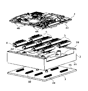
Figures 1-3 illustrate a circuit board assembly 1 comprising a heat sink 2
that is sandwiched
between first and second printed circuit boards (PCB) 3, 4.
The heat sink 2 is comprised from a material, typically a metal, having high
heat conductance;
aluminium and copper are suitable examples. In one preferred
Date Recue/Date Received 2023-06-23
CA 03149109 2022-01-28
WO 2021/018885
PCT/EP2020/071252
- 5 -
embodiment the heat sink comprises a solid block of metal such as one or more
of
aluminium, copper or titanium.
The heat sink 2 may be comprised from a cast, braised or machined piece.
Alternatively it may be made through an additive manufacture process.
The heat sink 2 has faces 2A 2B on opposite sides of the heat sink 2. Faces
2A, 2B
lie in direct contact with respective inner facing sides 3A, 4Aof PCBs 3, 4 to
provide
good thermal connection to the PCBs 3, 4. Faces 2A 2B are profiled to provide
a
pattern of recesses that correspond in shape and position to the components,
e.g.
microchips and other discreet electronic components, that are mounted to the
respective sides 3A 4A of the PCBs 3,4. This increases the contact area with
the
PCBs 3,4 or at least allows the heat sink 2 to more closely surround the heat
generating components on the PCBs to improve heat transfer from the PCBs 3,4
to
the heat sink 2.
The heat sink 2 defines internal channels 2C, visible in Fig 3, that provides
a
pathway, e.g. a circuitous pathway, for a coolant fluid, such as air or water,
to flow
through the heat sink 2. This provides means to increase the rate at which
heat can be
dissipated from the heat sink 2.
The internal channels 2C may be connected into a coolant system (not shown)
comprising, for example, a pump or fan to move the coolant fluid (liquid
and/or
gas)through the heat sink 2, and optionally also through a heat exchanger
which is
separate from the heat sink 2 to cool the coolant. The coolant system will
generally be
of conventional form and so further details of its structure and operation
will not be
described further.
The heat sink 2 comprises a number of (in this example eight though the number
may
vary) further internal channels 2D, see Figs 3 & 5, that extend through the
heat sink 2
between the first and second PCBs 3,4.
CA 03149109 2022-01-28
WO 2021/018885
PCT/EP2020/071252
- 6 -
The further internal channels 2D provide conduits for interconnecting cables 5
(in this
example eight cables, one per channel 2D, though the number may vary) that
connect
between the first and second PCBs 3,4. Each cable 5 may provide a power or
data
connection between the PCBs 3,4 or both power and data connections.
With reference to Fig 4, each cable 5 is comprised from a flexible film
substrate 5A
(e.g. of a electrically insulating polymer material) on which is printed, or
otherwise
disposed, a plurality of parallel electrically conductive traces 5B that
extend and
connect between terminals of board connectors 5C (header or socket) mounted at
opposite ends of the film substrate 5A. Each trace provides a single data or
power
connection. Each board connector 5C is arranged to mate with a corresponding
board
connector 3B, mounted on respective PCB 3,4.
The flexible film substrate 5A allows for relative movement between the board
connectors 5C to compensate for misalignment between the connectors 3B 4B of
the
respective PCB 3,4 in the X axis of the inner faces 3A 4A shown in Fig 3.
However
the width of the film substrate 5A means greater force is required to move the
board
connectors 5C through the Y axis of the inner faces 3A 4A.Where the film
substrate
5A carries many traces, the width of the substrate 5A may be such that the
force
required to move the conductor in the Y axis is too great to allow for blind-
mating
without applying a degree of force that could risk damaging the PCBs 3,4 or
connectors 5.
To address this, the flexible film substrate 5A is provided with multiple
slits 5D. Each
slit 5D lies between parallel traces 5B and extends parallel with the traces5B
for a
majority of their length. The slits 5D effectively create a series of narrow
parallel
cables, each carrying one or more conductive traces 5B, which can flex
independently
to the others and each more readily in the Y axis. This makes the cable 5 as a
whole
more flexible in the Y axis allowing for increased relative movement between
the
board connectors 5C.
CA 03149109 2022-01-28
WO 2021/018885
PCT/EP2020/071252
- 7 -
The flexibility of the film substrate 5A and the provision of the slits 5D
provide for
relative movement of the board-to-board connector 5C to compensate for any
misalignment between the connectors of the PCB's 3,4 in either X or Y axis
about the
face of the boards 3A 4A.
As can be seen most clearly in Figs 2 &5, when assembled, each cable 5 is
folded
over itself with board connectors 5C (header or socket) facing outwardly in
opposite
directions for connection to their counterparts 3B,4B on boards 3,4.
A spacer 6 is arranged directly between the board connectors 5C which acts to
provide a minimum separation distance between board connectors 5C of the same
cable 5.
With reference to Fig 5, the cable 5 comprises, at one end, at least one
aperture 5E
about which the end of the cable 5 is retained to the heat sink 2 by means of
a fastener
7, e.g. a threaded fastener. The fastener 7 passes through the aperture 5E to
fix to a
portion 2B of the heat sink 2 that protrudes into the space between the board
connectors of the folded over cable 5.
There is further provided a bearing spacer 8 that is retained between the
fastener 7
and the cable 5. The bearing spacer 8 has a narrower portion 8A that lies
within the
aperture 5E of the flexible substrate 5A and a broader portion 8B sandwiched
between a head 7A of the fastener and the cable 5.The spacing between the
broader
portion 8B and the heat sink 2, within which the cable 5 lies, and which is
dictated by
the height of the narrower portion 8A, is set to inhibit movement of the cable
at its
fastening point, and thus also of the board connector 5A proximate the
fastener 7,
away from the heat sink 2 whilst still allowing relative movement in the X and
Y
axes.
CA 03149109 2022-01-28
WO 2021/018885
PCT/EP2020/071252
- 8 -
The narrower portion 8A is narrower than the aperture 5E, such as to provide
free
space 9 between wall 5F of cable 5 facing the aperture5E and the narrower
portion
8A.
Through this arrangement one of the board connectors 5C of each cable 5 is
held in a
floating configuration, confined in the direction normal to face 4A of the
second
board 4, but free to move relative to the fastener, and thus about the X and Y
axis in
order to allow alignment with the PCB's connectors 4B.
To assemble, one end of each cable 5 is retained to heat sink 2 using
fasteners 7 as
described above. The board connectors 5A at each of the free ends of the cable
5, i.e.
the ends not mounted to the heat sink 2, are individually mated to their
corresponding
connector 3B on the first board 3. The heat sink 2 and first board 3are
brought
together and affixed with fasteners and/or heat conductive bonding adhesive,
e.g. heat
conductive epoxy.
The second board 4 is brought against the other side of the heat sink 2 (or
vice-versa)
.. so that the exposed board connectors 5C within the apertures 2D are
substantially
aligned with the corresponding connectors 4B on the second board 4. The
floating
character of the board connectors 5C allow the board connectors 5C to move
laterally
across the connector 4B in response to force applied to bring the connector 5C
4B
together to compensate for any initial misalignment between the two to ensure
the
two connector mate together correctly. This ability to blind-mate the
connectors 5C
4B makes it possible to mate multiple board connectors 5C to the second board
3
simultaneous using short board connectors 5.
It would be possible to connect both ends of each cable 5 to the heat sink 2
using the
fasteners 7 and spacing bearing 8 arrangement described earlier. Nevertheless
this is
considered unnecessary as through the afore described method the board
connectors
5C at the free ends of the cables 5 can be manipulated individually by virtue
of the
flexibility of the cable 5 and mated to the first board 3 before the first
board 3 and
heat sink 2 are bonded together. This contrasts when subsequently bonding the
CA 03149109 2022-01-28
WO 2021/018885
PCT/EP2020/071252
- 9 -
second board 4 to the heat sink 2 because unless the cables 5 are very much
longer
than apertures 2D (which would be difficult to house within the apertures 2D,
it is
difficult to manipulate multiple cable connectors 5C whilst simultaneously
mounting
the second board 4.
In an example application the circuit board assembly 1 forms part of a radar
system.
The first PCB 3 carries circuitry that provides an array of antenna elements
of an
electronically scanned array, said elements provided on an outer facing (i.e.
facing
away from the heat sink 2) surface 3C of the first PCB 3. The first PCB 3 also
carries
transmit and/or receive modules that amplify and/or change the phase and/or
timing
of signals to be transmitted and/or have been received from the antenna
elements.
The second PCB 4 carries power circuitry used to power the circuitry on the
first PCB
3, as well as higher level control circuitry for controlling the transmit
and/or receive
modules.
The cables 5 act to carry both control signals from the higher level control
circuitry to
the transmit and/or receive modules and also power from the power circuitry on
the
second PCB 4 to the circuitry of the first PCB 3.
It will be appreciated that the second board 4 may instead carry the antenna
elements
and transmit/receive modulated and the first board 3 carries the power
circuitry and
the higher level control circuitry.
The sandwich arrangement of the circuit boards and heat sink 2 provides a
compact
arrangement which is advantageous where the radar system is to be mounted
where
space is limited such as, for example, in the nose of an aerial platform, e.g.
an
aeroplane or helicopter.