Note : Les descriptions sont présentées dans la langue officielle dans laquelle elles ont été soumises.
WO 2021/046649
PCT/CA2020/051226
1
HIGH FREQUENCY WIRELESS POWER TRANSFER SYSTEM, TRANSMITTER AND
RECEIVER THEREFOR
Field
5 [0001] The subject disclosure relates generally to wireless power
transfer and in
particular, to a high frequency wireless power transfer system, transmitter
and receiver
therefor.
Background
10 [0002] Wireless charging and wireless power transfer systems are
becoming an
increasingly important technology to enable the next generation of devices.
The potential
benefits and advantages offered by the technology is evident by the increasing
number of
manufacturers and companies investing in the technology.
[0003] A variety of wireless power transfer systems
are known. A typical wireless
15 power transfer system includes a power source electrically connected to
a wireless power
transmitter, and a wireless power receiver electrically connected to a load.
[0004] In magnetic induction systems, the
transmitter has a coil with a certain
inductance that transfers electrical energy from the power source to a
receiving coil with a
certain inductance. Power transfer occurs due to coupling of magnetic fields
between the
20 inductors of the transmitter and receiver. The range of these magnetic
induction systems
is limited, and the inductors of the transmitter and receiver must be in
optimal alignment
for power transfer.
[0005] There also exist resonant magnetic systems
in which power is transferred due
to coupling of magnetic fields between the inductors of the transmitter and
receiver. In
25 resonant magnetic systems the inductors are resonated using at least one
capacitor. In
resonant magnetic systems, the transmitter is self-resonant and the receiver
is self-
resonant. The range of power transfer in resonant magnetic systems is
increased over
that of magnetic induction systems and alignment issues are rectified. While
electromagnetic energy is produced in magnetic induction and resonant magnetic
30 systems, the majority of power transfer occurs via the magnetic field.
Little, if any, power
is transferred via electric induction or resonant electric induction.
[0006] The Qi wireless charging standard is an
exemplary implementation of a
magnetic induction system. The Qi wireless charging standard is used in low
power
consumer electronics such as smart phones and wearable devices. Furthermore,
low cost
35 power converters, coils and integrated circuit are available for use in
the Qi wireless
CA 03150958 2022-3-11
WO 2021/046649
PCT/CA2020/051226
2
charging standard. The Qi wireless charging standard operates in the kHz
frequency
range. Accordingly, devices operating according to the Qi wireless charging
standard
have limited coupling range, require precise coil alignment and use ferrite-
based coils,
which can be heavy and fragile. Consequently, the application scope of the Qi
wireless
5 charging standard is limited.
[0007] In electric induction systems, the
transmitter and receiver have capacitive
electrodes. Power transfer occurs due to coupling of electric fields between
the capacitive
electrodes of the transmitter and receiver. Similar, to resonant magnetic
systems, there
exist resonant electric systems in which the capacitive electrodes of the
transmitter and
10 receiver are made resonant using at least one inductor. In resonant
electric systems, the
transmitter is self-resonant and the receiver is self-resonant. Resonant
electric systems
have an increased range of power transfer compared to that of electric
induction systems
and alignment issues are rectified. While electromagnetic energy is produced
in electric
induction and resonant electric systems, the majority of power transfer occurs
via the
15 electric field_ Little, if any, power is transferred via magnetic
induction or resonant
magnetic induction.
[0008] Applications of magnetic and electric
induction systems, commonly referred to
as inductive power transfer (IPT) systems, may operate in the tens of MHz
frequency
range. In the tens of MHz frequency range, the topology of direct current (DC)
to
20 alternating current (AC) inverters used in transmitters of these systems
are generally
based on Class E or Class EF2 inverter configurations. While these
configurations are
power efficient and simple to construct, optimum switching operation may only
be
maintained for a fixed load. Therefore, such configurations are highly
dependent on the
fixed load. Consequently, IPT systems using Class E or Class EF2 inverters
generally
25 only operate efficiently at a fixed coil separation distance and through
a narrow load
range.
[0009] As described in "Load-independent Class E
Power Inverters: Part I.
Theoretical Development" authored by R. E. Zulinski and K. J. Grady IEEE
Trans. Circuits
Syst. I, Reg. Papers, vol. 37, no. 8, pp. 1010-1018. Aug. 1990 and "Design of
Single-
30 switch Inverters for Variable Resistance/load Modulation Operation"
authored by L.
Roslaniec, A. S. Jurkov, A. Al Bastami, and D. J. Perreault in IEEE Trans.
Power
Electron., vol. 30, no. 6, pp. 3200-3214, Jun. 2015, the relevant portions of
which are
incorporated herein by reference, Class E and Class EF2 inverters may be
designed such
that they achieve zero-voltage switching (ZVS) and produce a constant output
voltage as
35 the load resistance varies when used with a finite DC inductor instead
of a choke.
CA 03150958 2022-3-11
WO 2021/046649
PCT/CA2020/051226
3
[0010] Such designs may extend the load range that
Class E or Class EF2 inverters
may operate efficiently from infinite load resistance (open circuit) to a
certain minimum
load resistance. While these designs may be applied to several applications,
such as high
frequency DC/DC converters, they cannot generally be used efficiently in IPT
systems
5 where the distance changes between the coils/electrodes. In IPT systems,
the load
ranges from zero resistance (short circuit) when the coils/electrodes are
completely
separated from each other to a certain maximum load resistance when the
coils/electrodes are closest to each other.
[0011] As previously stated, IPT systems may
operate in the tens of MHz frequency
10 range. Switching in the tens of MHz frequency range may be achieved by
utilizing wide-
bandgap devices such as GaN and SIC. As described in "Load-independent Class
E/EF
Inverters and Rectifiers for MHz-Switching Applications" authored by S.
Aldhaher, D. C.
Yates, and P. D. Mitcheson in IEEE Trans. Power Electron., vol. 33, no. 10,
pp. 8270-
8287, Oct. 2018 and "High-frequency, High-power Resonant Inverter with eGaN
FET for
15 Wireless Power Transfer' authored by J. Choi, D. Tsukiyama, Y. Tsuruda,
and J. M. R.
Davila in IEEE Trans. Power Electron., vol. 33, no. 3, pp. 1890-1896, March
2018, the
relevant portions of which are incorporated herein by reference, recent
developments in
resonant converters and soft-switching topologies, such as Class E and Class
EF, allow
for true exploitation of wide-bandgap devices and give designers topologies
and circuit
20 configurations to use for achieving high performance/power density
converters.
[0012] Operating at the tens of MHz frequency for
wireless power transfer increases
the maximum air gap distance, improves the tolerance to coil misalignment and
therefore,
allows a receiver to be placed anywhere in a charging zone without the
requirement for
precise alignment. This wireless power transfer also allows for high-Q, single-
turn air-core
25 coils to be used which are lightweight, compact and could be implemented
on low cost
FR4 PCBs. Such features were demonstrated by wirelessly powering a miniature
drone
as described in "Light-weight Wireless Power Transfer for Mid-air Charging of
Drones"
authored by S. Aldhaher, P. D. Mitcheson, J. M. Arteaga, G. Kkelis, and D. C.
Yates in
11th European Conf. Antennas Propagation, Mar. 2017, pp. 336-340, the relevant
30 portions of which are incorporated herein by reference.
[0013] Although wireless power transfer techniques
are known, improvements are
desired. It is therefore an object to provide a novel wireless power transfer
system, a
transmitter and receiver therefor and a method of wirelessly transmitting
power.
CA 03150958 2022-3-11
WO 2021/046649
PCT/CA2020/051226
4
Summary
[0014] It should be appreciated that this Summary
is provided to introduce a selection
of concepts in a simplified form that are further described below in the
Detailed
Description of Embodiments. This Summary is not intended to be used to limit
the scope
5 of the claimed subject matter.
[0015] Accordingly, in one aspect there is provided
a load independent inverter
comprising a switched mode zero-voltage switching (ZVS) amplifier comprising:
a pair of
circuits comprising: at least a transistor and at least a capacitor arranged
in parallel; and
at least an inductor arranged in series with the transistor and capacitor;
only one ZVS
10 inductor connected to the pair of circuits; and at least a pair of
capacitors connected to
the ZVS inductor and arranged in series with at least an inductor and at least
a resistor.
[0016] In one or more embodiments, the load
independent inverter comprises at least
two capacitors connected to the ZVS inductor. In one or more embodiments, the
at least
two capacitors are arranged in series with the at least one inductor and
resistor.
15 [0017] In one or more embodiments, a minimum value of a load
resistance
normalized to a characteristic impedance of the switched mode ZVS amplifier is
between
0.585 and 0.975.
[0018] In one or more embodiments, a q value of the
load independent inverter is
between 0.739 and 1.231.
20 [0019] In one or more embodiments, a residual reactance normalized
to a
characteristic impedance of the load independent inverter is between 0.194 and
0.323.
[0020] In one or more embodiments, a voltage gain
value of the load independent
inverter is between 2.349 and 3.915.
[0021] In one or more embodiments, a normalized
output power of the load
25 independent inverter is between 4.700 and 7.834.
[0022] In one or more embodiments, the load
independent inverter has constant
voltage output. In one or more embodiments, the load independent inverter has
a load
range of 5.625 ohms to an infinite or open circuit load. In one or more
embodiments, the
load independent inverter further comprises an impedance inverter circuit
configured to
30 convert the load independent inverter from constant voltage output to
constant current
output.
[0023] In one or more embodiments, the load
independent inverter has a constant
current output. In one or more embodiments, the load independent inverter has
a load
range of zero ohms or a short circuit load to 9.375 ohms.
CA 03150958 2022-3-11
WO 2021/046649
PCT/CA2020/051226
[0024] In one or more embodiments, the load
independent inverter is configured to
detect a metal object. In one or more embodiments, the load independent
inverter further
comprises: a peak detection circuit configured to measure a peak value of
voltage across
a transistor of the load independent inverter; and a comparator configured to
compare the
5 peak value of voltage with a threshold voltage and output a detection
signal if the peak
value of voltage exceeds the threshold voltage. In one or more embodiments,
the load
independent inverter further comprises: a voltage divider configured to
convert the peak
value of voltage prior to measurement by the peak detection circuit.
[0025] In one or more embodiments, the switched
mode ZVS amplifier is a radio
10 frequency (RF) amplifier.
[0026] In one or more embodiments, the load
independent inverter is a class E
inverter.
[0027] In one or more embodiments, the load
independent inverter is a direct current
(DC) to alternating current (AC) inverter.
15 [0028] According to another aspect there is provided a transmitter
comprising: a load
independent inverter comprising a switched mode zero-voltage switching (ZVS)
amplifier;
and a transmitter coil or electrodes connected to the load independent
inverter, the
transmitter coil or electrodes configured to transfer power to a receiver via
magnetic or
electric field coupling.
20 [0029] In one or more embodiments, the transmitter is non-resonant
or not self-
resonant.
[0030] In one or more embodiments, the transmitter
coil is configured to transfer
power via magnetic field coupling.
[0031] In one or more embodiments, the transmitter
electrodes are configured to
25 transfer power via electric field coupling.
[0032] In one or more embodiments, the transmitter
further comprises a power
source.
[0033] In one or more embodiments, the transmitter
further comprises a power
converter configured to convert a power signal from the power source prior to
receipt by
30 the inverter.
[0034] According to another aspect there is
provided a wireless power transfer
system comprising: a transmitter comprising: a load independent inverter
comprising a
switched mode zero-voltage switching (ZVS) amplifier, and a transmitter coil
or electrodes
connected to the load independent inverter, the transmitter coil or electrodes
configured
35 to transfer power to a receiver via magnetic or electric field coupling;
and the receiver
CA 03150958 2022-3-11
WO 2021/046649
PCT/CA2020/051226
6
comprising: a receiver coil or electrodes configured to extract power from the
receiver via
magnetic or electric field coupling.
[0035] In one or more embodiments, the transmitter
is non-resonant or not self-
resonant, and the receiver is resonant. In one or more embodiments, the
receiver is
5 resonant at an operating frequency of the transmitter.
[0036] In one or more embodiments, the transmitter
coil is configured to transfer
power via magnetic field coupling and the receiver coil is configured to
extract power via
magnetic field coupling.
[0037] In one or more embodiments, the transmitter
electrodes are configured to
10 transfer power via electric field coupling and the receiver electrodes
are configured to
extract power via electric field coupling.
[0038] In one or more embodiments, the receiver
further comprises a rectifier
connected to the receiver coil or electrodes.
[0039] In one or more embodiments, the receiver
further comprises a load connected
15 to the receiver coil or electrodes.
Brief Description of the Drawings
[0040] Embodiments will now be described more fully
with reference to the
accompanying drawings in which:
20 [0041] Figure 1 is a block diagram of a wireless power transfer
system;
[0042] Figure 2A is a block diagram of a resonant
magnetic wireless power transfer
system;
[0043] Figure 2B is a block diagram of a resonant
electric wireless power transfer
system;
25 [0044] Figure 3 is a block diagram a high frequency magnetic
wireless power transfer
system in accordance with an aspect of the subject disclosure;
[0045] Figure 4A is a partial schematic layout of
the inductive link of the high
frequency magnetic wireless power transfer system of Figure 3;
[0046] Figure 4B is a partial schematic layout of
the equivalent circuit seen by the
30 transmitter of the high frequency magnetic wireless power transfer
system of Figure 3;
[0047] Figure 5 is a schematic layout of the DC/AC
inverter of the high frequency
magnetic wireless power transfer system of Figure 3;
[0048] Figure 6 is an equivalent circuit of the
DC/AC inverter of Figure 5;
[0049] Figure 7 is a series of graphs of
simulations of the equivalent circuit of Figure
35 6;
CA 03150958 2022-3-11
WO 2021/046649
PCT/CA2020/051226
7
[0050] Figure 8 is a schematic layout of another
embodiment of the DC/AC inverter of
Figure 5;
[0051] Figure 9 is a schematic layout of another
embodiment of the DC/AC inverter of
Figure 5;
5 [0052] Figure 10 is a schematic layout of another embodiment of
the DC/AC inverter
of Figure 5;
[0053] Figure 11 is a block diagram of another
embodiment of the DC/AC inverter of
Figure 5;
[0054] Figure 12 is a block diagram of another
embodiment of the DC/AC inverter of
10 Figure 5; and
[0055] Figure 13 is a graph of the voltages at a
transistor of the DC/AC inverter of
Figure 12 when a metal object is present and not present.
Detailed Description of Embodiments
15 [0056] The foregoing summary, as well as the following detailed
description of certain
examples will be better understood when read in conjunction with the appended
drawings. As used herein, an element or feature introduced in the singular and
preceded
by the word "a" or "an" should be understood as not necessarily excluding the
plural of
the elements or features. Further, references to "one example" or "one
embodiment" are
20 not intended to be interpreted as excluding the existence of additional
examples or
embodiments that also incorporate the described elements or features.
Moreover, unless
explicitly stated to the contrary, examples or embodiments "comprising" or
"having" or
"including" an element or feature or a plurality of elements or features
having a particular
property may include additional elements or features not having that property.
Also, it will
25 be appreciated that the terms "comprises", "has", "includes" means
"including by not
limited to" and the terms "comprising", "having" and "including" have
equivalent meanings.
It will also be appreciated that like reference characters will be used to
refer to like
elements throughout the description and drawings.
[0057] As used herein, the terms "adapted" and
"configured" mean that the element,
30 component, or other subject matter is designed and/or intended to
perform a given
function. Thus, the use of the terms "adapted" and "configured" should not be
construed
to mean that a given element, component, or other subject matter is simply
"capable of
performing a given function but that the element, component, and/or other
subject matter
is specifically selected, created, implemented, utilized, and/or designed for
the purpose of
35 performing the function. It is also within the scope of the subject
application that
CA 03150958 2022-3-11
WO 2021/046649
PCT/CA2020/051226
8
elements, components, and/or other subject matter that are described as being
adapted
to perform a particular function may additionally or alternatively be
described as being
configured to perform that function, and vice versa. Similarly, subject matter
that is
described as being configured to perform a particular function may
additionally or
5 alternatively be described as being operative to perform that function.
[0058] It will be understood that when an element
is referred to as being "on,"
"attached" to, "connected" to, "coupled" with, "contacting," etc., another
element, it can be
directly on, attached to, connected to, coupled with or contacting the other
element or
intervening elements may also be present.
10 [0059] It should be understood that use of the word "exemplary",
unless otherwise
stated, means 'by way of example' or 'one example', rather than meaning a
preferred or
optimal design or implementation.
[0060] Unless defined otherwise, all technical and
scientific terms used herein have
the same meaning as is commonly understood by one of skill in the art to which
the
15 subject disclosure pertains.
[0061] For the purposes of the subject disclosure,
switching frequency, cos, is defined
as the frequency at which switches are turned on and off. The switching
frequency may
be supplied from an external signal source, such as a function generator, or
generated
using an oscillator. A switching signal, based on the switching frequency, is
the main
20 "clock" of a wireless power transfer system. Therefore, the fundamental
frequency
components of all other voltage and current signals of related elements will
be equal to
the switching frequency.
[0062] For the purposes of the subject disclosure,
resonant frequency, coo, is defined
as the frequency at which a circuit network has a zero reactive impedance. The
resonant
25 frequency of a series LCR circuit is given by equation 1:
1
4.0
.%=/"1
(1)
where L is the inductance and C is the capacitance.
[0063] The resonant frequency of a parallel RLC
circuit is given by equation 2:
1
1
= V th
2
(2)
30 where R is the load. The switching frequency is not necessarily equal to
the resonant
frequency. Different modes of operation can be obtained by operating an
inverter at
switching frequencies above, below or equal to the resonant frequency.
CA 03150958 2022-3-11
WO 2021/046649
PCT/CA2020/051226
9
[0064] For the purposes of the subject disclosure,
ZVS is switching of a transistor
from an off state to an on state when the voltage across the transistor is
zero.
Consequently, there is no energy lost during this transition from the off to
the on state. In
practice, there is some energy lost due to the finite time of the transition
period. However,
5 the energy loss is substantially lower than a non-ZVS circuit. ZVS
allows for efficient
operation of power inverters, especially at MHz frequency ranges. ZVS is
achieved by
using a combination of passive components such as capacitors and inductors
with certain
values.
[0065] For the purposes of the subject disclosure,
characteristic impedance (Z0) of a
10 resonant network of an inverter is given by equation 3:
L
1
(3)
where co is the frequency, L is the inductance of the resonant network of the
inverter and
C is the capacitance of the resonant network.
[0066] Turning now to Figure 1, a wireless power
transfer system generally identified
15 by reference numeral 100 is shown. The wireless power transfer system
100 comprises a
transmitter 110 comprising a power source 112 electrically connected to a
transmit
element 114, and a receiver 120 comprising a receive element 124 electrically
connected
to a load 122. Power is transferred from the power source 112 to the transmit
element
114. The power is then transferred from the transmit element 114 to the
receive element
20 124 via resonant or non-resonant electric or magnetic field coupling.
The power is then
transferred from the receive element 124 to the load 122.
[0067] Turning now to Figure 2& an IPT system is
shown. In this embodiment, the
IPT system is a resonant magnetic wireless power transfer system generally
identified by
reference numeral 200. The resonant magnetic wireless power transfer system
200
25 comprises a transmitter 210 comprising a power source 212 electrically
connected to a
transmit resonator 214. The transmit resonator 214 comprises a transmit
resonator coil
216, electrically connected to the power source 212 via a capacitor 218. The
magnetic
resonant wireless power transfer system 200 further comprises a receiver 220
comprising
a receive resonator 224 electrically connected to a load 222. The receive
resonator 224 is
30 tuned to the resonant frequency of the transmit resonator 214. The
receive resonator 224
comprises a receive resonator coil 226, which is electrically connected to the
load 222 via
a capacitor 228.
CA 03150958 2022- 3- 11
WO 2021/046649
PCT/CA2020/051226
[0068] During operation of the resonant magnetic
wireless power transfer system
200, power is transferred from the power source 212 to the transmit resonator
coil 216 via
the capacitors 218. In particular, the power signal from the power source 212
that is
transmitted to the transmit resonator coil 216 via the capacitors 218 excites
the transmit
5 resonator 214 causing the transmit resonator 214 to generate a magnetic
field. When the
receiver 220, which is tuned to the same resonant frequency as the transmitter
210, is
placed within the magnetic field, the receive resonator 224 extracts power
from the
transmit resonator 214 via resonant magnetic field coupling. The extracted
power is then
transferred from the receive resonator 224 to the load 222. As the power
transfer is highly
10 resonant, the transmit resonator and receive resonator coils 216 and
226, respectively,
need not be as close together or as well aligned as is the case with a non-
resonant
magnetic system. While the transmit resonator 214 may generate an electric
field, little, if
any, power is transmitted via electric field coupling.
[0069] Turning now to Figure 2B, another IPT system
is shown. In this embodiment,
15 the IPT system is a resonant electric wireless power transfer system
generally identified
by reference numeral 250. The resonant electric wireless power transfer system
250
comprises a transmitter 260 comprising a power source 262 electrically
connected to a
transmit resonator 264. The transmit resonator 264 comprises transmit
resonator
electrodes 266, which are electrically connected to the power source 262 via
one or more
20 inductors 268. The resonant electric wireless power transfer system 250
further
comprises a receive 270 comprising a receive resonator 274 electrically
connected to a
load 272. The receive resonator 274 is tuned to the resonant frequency of the
transmit
resonator 264. The receive resonator 274 comprises receive resonator
electrodes 276,
which are electrically connected to the load 272 via one or more inductors
278.
25 [0070] During operation of the resonant electric wireless power
transfer system 250,
power is transferred from the power source 262 to the transmit resonator
electrodes 266
via the inductors 268. In particular, the power signal from the power source
262 that is
transmitted to the transmit resonator electrodes 266 via the inductors 268
excites the
transmit resonator 264 causing the transmit resonator 264 to generate an
electric field.
30 When the receiver 270, which is tuned to the same resonant frequency as
the transmitter
260, is placed within the electric field, the receive resonator 274 extracts
power from the
transmit resonator 264 via resonant electric field coupling. The extracted
power is then
transferred from the receive resonator 274 to the load 272. As the power
transfer is highly
resonant, the transmit resonator and receive resonator electrodes 266 and 276,
35 respectively, need not be as close together or as well aligned as is the
case with a non-
CA 03150958 2022-3-11
WO 2021/046649
PCT/CA2020/051226
11
resonant electric system. While the transmit resonator 264 may generate a
magnetic
field, little, if any, power is transmitted via magnetic field coupling.
[0071] Turning now to Figure 3, a high frequency
wireless power transfer system in
accordance with an aspect of the subject disclosure and generally identified
as reference
5 numeral 300 is shown. The high frequency wireless power transfer system
300 comprises
a transmitter 302 and a receiver 304. As will be described, the high frequency
wireless
power system 300 operates by transferring power from the transmitter 302 that
is non-
resonant or not self-resonant to a receiver 304 resonating at the operating
frequency of
the transmitter 302.
10 [0072] The transmitter 302 is configured to transmit power
wirelessly via high
frequency magnetic inductive coupling as will be described. While an electric
field may
also be generated, little, if any, power is transferred via electric field
coupling.
[0073] The transmitter 302 comprises a power source
306, a transmitter DC/DC
converter 308, a DC/AC inverter 310 and transmitter coil 312. The power source
306 is
15 electrically connected to the transmitter DC/DC converter 308. The power
source 306 is
configured to generate a DC power signal. The power source 306 is configured
to output
the DC power signal to the transmitter DC/DC converter 308. In this
embodiment, the DC
power signal is between 24 V and 48 V. The transmitter DC/DC converter 308 is
electrically connected to the power source 306. The transmitter DC/DC
converter 308 is
20 electrically connected to the DC/AC inverter 310. The transmitter DC/DC
converter 308
interfaces the power source 306 to the DC/AC inverter 310. The transmitter
DC/DC
converter 308 is configured to convert the DC power signal from the power
source 306 to
a voltage level for transmission to the DC/AC inverter 310.
[0074] The DC/AC inverter 310 is electrically
connected to the transmitter DC/DC
25 converter 308. The DC/AC inverter 310 is electrically connected to the
transmitter coil
312. The DC/AC inverter 310 is configured to convert the DC power signal from
the
transmitter DC/DC converter 308 into a sinusoidal radio frequency (RE) power
signal. The
sinusoidal RE power signal is output from the DC/AC converter 310 to the
transmitter coil
312.
30 [0075] While the transmitter 302 has been described as comprising
the transmitter
DC/DC converter 308, one of skill in the art will appreciate that other
configurations are
possible. In another embodiment, the transmitter 302 does not comprise the
transmitter
DC/DC converter 308. In this embodiment, the power source 306 is electrically
connected
to the DC/AC inverter 310. The power source 306 is configured to generate a DC
power
35 signal that is acceptable to the DC/AC inverter 310.
CA 03150958 2022-3-11
WO 2021/046649
PCT/CA2020/051226
12
[0076] The receiver 304 is configured to extract
power from the transmitter 302 via
high frequency magnetic inductive coupling as will be described. While an
electric field
may also be generated, little, if any, power is extracted via electric field
coupling.
[0077] The receiver 304 comprises a receiver coil
314, an AC/DC rectifier 316, a
5 receiver DC/DC converter 318 and a load 320. The receiver coil 314 is
electrically
connected to the AC/DC rectifier 316. The receiver coil 314 is configured to
receive power
from the transmitter 302 via the transmitter coil 312 using high frequency
magnetic
coupling. In this embodiment, the receiver coil 314 has identical dimensions
and number
of turns as the transmitter coil 312.
10 [0078] The AC/DC rectifier 316 is electrically connected to the
receiver coil 314. The
AC/DC rectifier 316 is electrically connected to the receiver DC/DC converter
318. The
AC/DC rectifier 316 is configured to convert sinusoidal RF power signal from
the receiver
coil 314 to a DC power signal. The AC/DC rectifier 316 is configured to output
the DC
power signal to the receiver DC/DC converter 318.
15 [0079] The receiver DC/DC converter 318 is electrically connected
to the AC/DC
rectifier 316. The receiver DC/DC converter 318 is electrically connected to
the load 320.
The DC power signal is output from the AC/DC rectifier 316 to the receiver
DC/DC
converter 318. The receiver DC/DC converter 318 interfaces the AC/DC rectifier
316 to
the load 320. The receiver DC/DC converter 318 is configured to convert the
received DC
20 power signal. The converted DC power signal is output from the receiver
DC/DC
converter 318 to the load 320. The load 320 is electrically connected to the
receiver
DC/DC converter 318. The load 320 may be a fixed or a variable load.
[0080] While the receiver 304 has been described as
comprising the receiver DC/DC
converter 318, one of skill in the art will appreciate that other
configurations are possible.
25 In another embodiment, the receiver 304 does not comprise the receiver
DC/DC
converter 318. In this embodiment, the AC/DC rectifier 316 is electrically
connected to the
load 320. The AC/DC rectifier 316 is configured to generate a DC power signal
that is
acceptable to the load 320.
[0081] The transmitter 302 operates at a given
frequency. In this embodiment, the
30 operating frequency of the transmitter 302 is 13.56 MHz. Furthermore, in
this
embodiment, the transmitter coil 312 and receiver coil 314 each have
dimensions of 23.4
cm x 26.2 cm. The coils 312 and 314 each consist of two tums of copper traces
having a
width of 14 mm on a FR4 printed circuit board (PCB). The coils 312 and 314
have an
inductance of approximately 1.50 uH. The reflected load seen by the
transmitter coil 312
CA 03150958 2022-3-11
WO 2021/046649
PCT/CA2020/051226
13
varies from 0 ohms, at no load 320, to 7 ohms at full load 320. The maximum
power
required by the load 320 is 30 W.
[0082] The receiver 304 operates at a given
frequency. In this embodiment, the
operating frequency of the receiver 304 is the operating frequency of the
transmitter 302.
5 In this embodiment, the operating frequency of the receiver 304 is 13.56
MHz.
[0083] As previously stated, the DC/AC inverter 310
is configured to convert the DC
power signal from the transmitter DC/DC converter 308 into a sinusoidal RE
power signal.
The sinusoidal RE power signal is output from the DC/AC converter 310 to the
transmitter
coil 312.
10 [0084] In particular, the DC/AC inverter 310 drives the
transmitter coil 312 with a
sinusoidal alternating current (AC). The transmitter coil 312 is configured to
generate an
inductive (magnetic) field and to transfer power via high frequency inductive
(magnetic)
field coupling. The DC/AC inverter 310 takes a DC input voltage and converts
it to a high
frequency AC current to drive the transmitter coil 312.
15 [0085] The DC/AC inverter 310 is affected by changes to loading
conditions, changes
in geometry of the system 300 and external distances (i.e. environmental
effects), such
as the presence of metallic objects near the system 300. It is desirable
therefore that the
DC/AC inverter 310 is robust and tolerant to these changes and also that the
DC/AC
inverter 310 operates in MHz frequencies.
20 [0086] As previously stated, Class E and Class EF2 inverters may
be designed such
that they achieve ZVS and produce a constant output voltage as the load
resistance
varies when used with a finite DC inductor instead of a choke. Such designs
may extend
the load range that Class E or Class EE2 inverters may operate efficiently
from infinite
load resistance (open circuit) to a certain minimum load resistance. While
these designs
25 may be applied to several applications, such as high frequency DC/DC
converters, they
cannot generally be used efficiently in the high frequency wireless power
transfer system
300 as the distance changes between the coils 312 and 314, and as the load
ranges from
zero resistance (short circuit) when the coils 312 and 134 are completely
separated from
each other to a certain maximum load resistance when the coils 312 and 314 are
closest
30 to each other.
[0087] Furthermore, in some applications of IPT
systems that operate at tens of MHz,
the topology of the DC/AC inverter 310 is based on a Class E or Class E2
configuration as
described in "Load-independent Class E/EF Inverters and Rectifiers for MHz-
Switching
Applications" authored by S. Aldhaher, D. C. Yates, and P. D. Mitcheson in
IEEE Trans.
35 Power Electron., vol. 33, no. 10, pp. 8270-8287, Oct. 2018 and
"Maximizing DC-to-load
CA 03150958 2022-3-11
WO 2021/046649
PCT/CA2020/051226
14
Efficiency for Inductive Power Transfer" authored by M. Pinuela, D. C. Yates,
S.
Lucyszyn, and P. D. Mitcheson in IEEE Trans. Power Electron., vol. 28, no. 5,
pp. 2437-
2447, May 2013, the relevant portions of which are incorporated herein by
reference.
While these configurations are power efficient and simple to construct, they
can only
5 maintain their optimum switching operation for a fixed load and
therefore are highly
dependent on the load value.
[0088] Consequently, this limits an IPT system with
a Class E or Class EF2 DC/AC
inverter to function efficiently only at a fixed coil separation distance and
for a narrow load
range.
10 [0089] To overcome the previously discussed challenges when using
inverters based
on Class E or Class EF2 configurations, and to allow for variable distance
between the
transmitter and receiver coils 312 and 314, the DC/AC inverter 310 is load
independent.
The load independent DC/AC inverter 310 allows Class E and Class EF inverters
to
maintain efficient operation by achieving ZVS regardless of the load
resistance value. In
15 addition, unlike the typical Class E and Class EF2, the load independent
Class E and
Class EF inverters can deliver a constant output AC voltage or current that
does not
change with load which is more suitable for IPT applications.
[0090] A discussion of the efficiency of the
coupling and/or inductive link between the
coils 312 and 314 is beneficial when considering the design of the DC/AC
inverter 310.
20 As previously stated, the high frequency wireless power transfer system
300 comprises
the transmitter 302 and the receiver 304. The transmitter 302 comprises, among
other
elements, the transmitter coil 312, and the receiver 304 comprises, among
other
elements, the receiver coil 314.
[0091] The coils 312 and 314 are separated from
each other by a certain gap. The
25 transmitter coil 312 is driven with a sinusoidal AC at a certain fixed
frequency, the
operating frequency of the transmitter 302. An alternating magnetic field is
generated
which couples to the receiver coil 314 and induces a sinusoidal voltage across
the
terminals of the receiver coil 314 with the same frequency of the current in
the transmitter
coil 312. Any load connected across the terminals of the receiver coil 314,
such as the
30 load 320, will result in electric current flowing into the load. A
coupling coefficient k
indicates the amount of coupling between the two coils 312 and 314, as defined
in
equation 4:
¨
______________________________________________________________________________
L,
(4)
CA 03150958 2022-3-11
WO 2021/046649
PCT/CA2020/051226
where is L is the inductance of the transmitter coil 312, Ls is the inductance
of the
receiver coil 314 and M is the mutual inductance between the coils 312 and
314.
[0092]
Turning now to Figure 4A, a
partial schematic layout of the inductive link of the
high frequency magnetic wireless power transfer system 300 is shown. Figure 4A
5
includes a circuit representation of the two
coupled coils 312 and 314. A resistor 402 with
a resistance IRL represents the AC load resistance. A capacitor 404 with a
capacitance Cs
is connected in series with the receiver coil 314 in order to resonate the
receiver coil 314
at the operating frequency. The reflected impedance, ZRef, seen by the
transmitter coil
312 is given by equation 5:
L;i2:112
%BA = 1?!.
¨ ;Ole =
10
(5)
where M is the mutual inductance between the coils 312 and 314, w is the
operating
frequency, p(s is the impedance of the receiver coil 314 at the frequency of
operation and
jXcs is the impedance of the series capacitor 404 at the frequency of
operation.
[0093]
The reflected impedance is a
measure of how much of the actual load is seen
15
by the transmitter 302. It is a function of the
mutual inductance between the coils 312 and
314, which is affected by the distance between the coils 312 and 314. The
closer the coils
312 and 314 are to each other, the higher the mutual inductance and the higher
the
reflected impedance. The further apart the coils 312 and 314 are from each
other, the
lower the mutual inductance and the lower the reflected impedance.
20 [0094]
As shown in equation 5, the reflected impedance
is inversely proportional to
the load resistance and magnitude of the impedance of the receiver coil 314.
Maximizing
the reflected impedance allows for power to be delivered to the load 320 at
lower
currents. Furthermore, the DC/AC inverter 310 can operate at lower currents,
and hence
has lower conduction and ohmic losses and high efficiency.
25 [0095]
The reflected impedance of equation 5 may be
maximized by cancelling the
reactance term Xi_s of the receiver coil 314. The reactance term reflects a
resistive load to
the transmitter 302. This can be done at the operating frequency by setting
the reactance
term to be equal to 1/(w2L8). With this capacitance value, equation 5 becomes
equation 6:
44.4 = /441
(6)
30 [0096]
Turning now to Figure 4B, a partial schematic
layout of the equivalent circuit
seen by the transmitter 302 of the high frequency magnetic wireless power
transfer
system 300 is shown. Figure 4B shows the equivalent circuit of the transmitter
coil 312
CA 03150958 2022-3-11
WO 2021/046649
PCT/CA2020/051226
16
when operating with a receiver coil 314 tuned at resonance (i.e. jXLs = gcs).
The circuit
comprises an inductor 406 with an inductance Lp and a resistor 408 with a
resistance
RRef. As seen in equation 6, when using series resonance, the reflected
impedance
remains resistive regardless of the bad resistance value. This is unlike the
case with a
5 parallel tuned receiver coil 314 or secondary coil as described in
"Inductive Powering:
Basic Theory and Application to Biomedical Systems" authored by K. V.
Schuylenbergh
and R. Puers, 1st ed. Springer Publishing Company, Incorporated, 2009, the
relevant
portions of which are incorporated herein by reference.
[0097] Reflected impedance remains resistive
ensuring that DC/AC inverter 310 is
10 not detuned away from optimum operating conditions. Series resonance,
however, can
limit the maximum frequency of operation as the parasitic capacitance of the
receiver coil
314 is not absorbed into the capacitor Cs that is resonant during operation.
[0098] As previously stated, while the receiver
coil 314 may be operating at
resonance or near resonance, the transmitter coil 312 is not operating at
resonance (i.e.
15 the transmitter coil 312 is not self-resonant). This is in contrast to
many IPT systems
where the transmitter coil 312 is operating at resonance.
[0099] From the above equations, the link
efficiency of the high frequency wireless
power transfer system 300 may be determined. The link efficiency of the high
frequency
wireless power transfer system 300 is defined as the power delivered to the AC
20 secondary load (the load 320) divided by the power input to the
transmitter coil 312. With
the receiver coil 314 operating at resonance and with the optimal load for
maximum
efficiency, the link efficiency (n) is given by equation 7:
A-2(b,
(1 + 14; +
(7)
25 where Qi.p and CiLs are the unloaded quality factors of the transmitter
coil 312 and the
receiver coil 314, respectively.
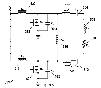
[0100] Turning now to Figure 5, a schematic diagram
of the DC/AC inverter 310 of
the high frequency magnetic wireless power transfer system 300 is shown. The
DC/AC
inverter 310 is configured to generate an AC output voltage with a constant
amplitude
30 regardless of load whilst maintaining ZVS.
[0101] As previously stated, the DC/AC inverter 310
is load independent. In this
embodiment, the DC/AC inverter 310 is a push-pull inverter. In this
embodiment, the
DC/AC inverter 310 is a class E inverter. The DC/AC inverter 310 has a voltage-
mode
CA 03150958 2022-3-11
WO 2021/046649
PCT/CA2020/051226
17
output. Voltage-mode output indicates that the DC/AC inverter 310 has a
constant voltage
output.
[0102] The DC/AC inverter 310 comprises a switched
mode ZVS amplifier as will be
described. The amplifier is a radio frequency (RE) amplifier.
5 [0103] As shown in Figure 5, the switched mode ZVS amplifier
comprises series
inductors 502 and 518 with inductances L1 and L2, respectively, that receive
an input
voltage tin. Each inductor 502, 518 is connected in series to a combination of
a transistor
512 and 520 (Q-, and at), respectively, (or switch) and capacitor 514 and 522.
The
capacitors 514 and 522 have capacitances C1 and C2, respectively.
Specifically, transistor
10 512 and capacitor 514 are arranged in parallel, and are connected to
inductor 502.
Transistor 520 and capacitor 522 are arranged in parallel and are connected to
inductor
518. Both transistor 512, 520 and capacitor 514, 522 pairs are grounded.
Inductor 516
with inductance Lzvs is connected in parallel between the inductors 502 and
518. Inductor
532 with inductance LREsa, capacitor 504 with capacitance C. inductor 506 with
15 inductance L3, resistor 508 with resistance R/_, capacitor 510 with
capacitance C3b, and
inductor 534 with inductance LREsb are arranged in series and connected in
parallel to
inductor 516. Inductor 506 represents the inductance of the transmitter coil
312 and
resistor 508 represents the reflected load of the receiver coil 314. Inductors
532, 534
represent the residual inductance of the receiver coil 314.
20 [0104] The state-space modelling approach as described in "Design
and optimization
of switched-mode circuits for inductive links" authored by S. Aldhaher in
Ph.D.
dissertation, Cranfield University, 2014, the relevant portions of which are
incorporated
herein by reference, was used in order to derive the design equations for the
DC/AC
inverter 310.
25 [0105] An equivalent circuit of the DC/AC inverter 310 illustrated
in Figure 5 was
produced as per the state-space modelling approach. Turning now to Figure 6,
the
equivalent circuit of the DC/AC inverter 310 is shown. As shown in Figure 6,
two voltage
sources 602 and 622 with voltages Vin feed signals into two inductors 604 and
624 with
inductances L1 on either side of the equivalent circuit. Specifically, one
voltage source
30 602 feeds into one inductor 604, and another voltage source 622 feeds
into another
inductor 624. Each voltage source 602, 622 and inductor 604, 624 pair is
connected to a
resistor 606 or 626 having a resistance R1 or R2, respectively, in a parallel
arrangement.
Each voltage source 602, 622 and inductor 604, 624 pair is further connected
to a
capacitor 608, 628 in a parallel arrangement. Each capacitor has a capacitance
Cy
35 Specifically, the voltage source 602 and inductor 604 pair is connected
to resistor 606
CA 03150958 2022-3-11
WO 2021/046649
PCT/CA2020/051226
18
and capacitor 608. The other voltage source 622 and inductor 624 pair is
connected to
resistor 626 and capacitor 628. The inductors 604 and 624 are connected in
series to an
inductor 610 having an inductance Lzvs and a resistor 612 having a resistance
RLzvs. The
inductor 610 and the resistor 612 are connected in parallel to capacitor 614
having a
5 capacitance Ca, inductor 616 having an inductance L2 and resistor 618
having an
resistance RL. The capacitor 614, inductor 616 and resistor 618 form an output
network.
The capacitance Ca of the capacitor 614 is equal to the sum of the capacitance
of the
capacitors 504 and 510 (C3a and Cab). The transistors 512 and 520 of Figure 5
have been
replaced with resistors 606 and 626 having resistances R1 and R2,
respectively.
10 [0106] The equivalent circuit of Figure 6 was simulated for load
values RL = 6.25,
12.5, 25 and 100 ohms. The results of these simulations are shown in the
graphs of
Figure 7. As shown in Figure 7, the ratio of the voltage of the
transistor/switch 512 to the
input voltage Vm is maximized when the load value RL is equal to 6.25 ohms.
Similarly,
the ratio of the voltage of the transistor/switch 520 to the input voltage Vgn
is maximized
15 when the load value RL is equal to 6.25 ohms.
[0107] Furthermore, as shown in Figure 7, the DC/AC
inverter 310 maintains ZVS for
different loading conditions from open circuit load condition to minimum load
resistance.
The amplitude and phase of the output AC voltage across the load remain
constant
regardless of load value. While the shape of the various waveforms may change,
ZVS is
20 generally maintained and the amplitude and phase of the output voltage
is generally
constant. Additionally, the current in the transistors 512 and 520 at turn off
has a negative
slope as the load resistance decreases. A negative slope at turn off may
minimize the
turn off time of the transistors 512 and 520 and may negate the effect of
parasitic
inductances.
25 [0108] As previously stated, the state-space modelling approach
was used to derive
design equations for the equivalent circuit of Figure 6. The design equations
discussed
may be used to build an AC/DC inverter 310 for a particular set of
requirements such as
load impedance, resonator impedance, frequency of operation and input DC
voltage. The
following design equations were derived: q value, residual reactance Xres,
voltage gain,
30 load resistance RL, and output power F.
[0109] The q value, which sets the resonant
frequency of the DC/AC inverter 310 to
the frequency of operation is given by equation 8:
1
= 0.965
(8)
CA 03150958 2022-3-11
WO 2021/046649
PCT/CA2020/051226
19
[0110] The q value is unique to each inverter class
and topology. For the operating
frequency of 13.56 MHz and optimum performance of the high frequency wireless
power
transfer system 300, the q value is approximately 0.985. This is expected, as
the
transmitter 302 is non-resonant (or not self-resonant) so the q value should
not be equal
5 to 1.
[0111] One of skill in the art will appreciate that
the q value may not be exactly equal
to 0.985, and the high frequency wireless power transfer system 300 may still
function;
however, the load range will be reduced and performance will be negatively
affected. In
some embodiments, the q value may vary by as much as plus or minus 25% of
0.985
10 (e.g. approximately 0.739 to 1.231) while still providing acceptable
performance.
[0112] The output network consisting of the
capacitor 614, inductor 616 and resistor
618 with the capacitance Ca of the capacitor 614 being equal to the sum of the
capacitance of the capacitor 504 and the capacitor 510 (C3 = C3a + Cs,) is not
tuned to the
resonant frequency of the transmitter 302. Consequently, the output network
will have a
15 residual reactance Xres at the frequency of operation given by equation
9:
(9)
[0113] Similar to the q value, the value of Xres is
unique for an inverter class and
topology. For the AC/DC inverter 310, the ratio of )(es normalized to the
characteristic
impedance of the inverter 310 is given by equation 10:
0.23$
Z.,
20
(10)
[0114] This is expected, as the transmitter 302 is
non-resonant (or not self-resonant)
so the Xres value should not be equal to zero (0). While not described, one of
skill in the
art will appreciate that a residual inductance may also be present as
represented by
inductors 532, 534 in Figure 5.
25 [0115] One of skill in the art will appreciate, that the Xres
value may not be exactly
equal to 0.258, and the high frequency wireless power transfer system 300 may
still
function; however, the performance will be negatively affected_ In some
embodiments, the
Xres value may vary by as much as plus or minus 25% of 0.258 (e.g.
approximately 0.194
to 0.323) while still providing acceptable performance.
30 [0116] The characteristic impedance of the AC/DC inverter 310 is
given by equation
11:
CA 03150958 2022-3-11
WO 2021/046649
PCT/CA2020/051226
Lay-,
;
ti ¨el =
(1 1)
[0117]
The voltage gain is the ratio of
the amplitude of the AC voltage across the load
RI_ to the input DC voltage VIN. For this AC/DC inverter 310, the voltage gain
is given by
equation 12:
1;7.
I I 3.
18-2
I IN
5
(12)
[0118]
For the operating frequency of
13.56 MHz and optimum performance of the
high frequency wireless power transfer system 300, the voltage gain is
approximately
3.132.
[0119]
One of skill in the art will
appreciate that the voltage gain value may not be
10
exactly equal to 3.132, and the high frequency
wireless power transfer system 300 may
still function; however, the performance will be negatively affected. In some
embodiments, the voltage gain value may vary by as much as plus or minus 25%
of
3.132 (e.g. approximately 2.349 to 3.915) while still providing acceptable
performance.
[0120]
As previously stated, the DC/AC
inverter 310 has a voltage-mode output, i.e. a
15
constant voltage output. The DC/AC inverter 310
may operate efficiently when the load
resistance RL is in the range of (Rumn, co). If the load resistance RI
decreases below Rumn,
the DC/AC inverter 310 will no longer operate efficiently, i.e. ZVS operation
will be lost,
and the output voltage of the DC/AC inverter 310 will vary.
[0121]
This is because the voltage
across the transistor will swing below zero volts
20
which in practice means that the body diodes of
the transistors ar and Q2 will conduct
and therefore disrupt the operation of the DC/AC inverter 310. The minimum
load
resistance Rum corresponds to the load at which the DC/AC inverter (when
operating at
voltage-mode) can deliver the maximum power. Here, the value of &awn
normalized to the
characteristic impedance Zo is given by equation 13:
RI. min =71. 0.760.
Zõ
25
(13)
[0122]
One of skill in the art will
appreciate, that the value of Ri_min normalized may not
be exactly equal to 0.780, and the high frequency wireless power transfer
system 300
may still function; however, the performance will be negatively affected. In
some
embodiments, the value of Rum normalized may vary by as much as plus or minus
25%
30 of 0.780 (e.g. between 0.585 and 0.975) while still providing acceptable
performance.
CA 03150958 2022-3-11
WO 2021/046649
PCT/CA2020/051226
21
[0123] Combining equations 12 and 13, the output
power Pout of the DC/AC inverter
310 at a minimum load resistance for a particular input DC voltage may be
determined.
The output power Pout normalized is given by equation 14:
Zo Pots 1 VAL 1
G¨
.2S7 sr. 2w
¨ viZ
5
(14)
[0124] One of skill in the art will appreciate,
that the output power Pow normalized
may not be exactly equal to 6.267, and the high frequency wireless power
transfer system
300 may still function; however, the performance will be negatively affected.
In some
embodiments, the output power Pout normalized may vary by as much as plus or
minus
10 25% of 6.267 (e.g. approximately 4.700 to 7.834) while still providing
acceptable
performance_
[0125] Implementing the DC/AC inverter 310
according to the derived design
equations yields a DC/AC inverter that is more efficient and robust than other
configurations. In particular, Table 1 lists differences between the DC/AC
inverter 310 and
15 other configurations.
CA 03150958 2022-3-11
WO 2021/046649
PCT/CA2020/051226
22
Table 1
GaN based,
DC/AC GaN based GaN
based
SIC based
Inverter 310 System 1
System 2
System
Class D (H-
Inverter Topology Class E Class EF2
Class EF
bridge)
Switch duty cycle 50% Fixed 30% Fixed
50% Fixed 30% Fixed
Number of
switches in push- 2 2
4 2
pull configuration
Deadtime control
No No
Yes No
requirement?
No of resonant
inductors in push-
1 6
2 2
pull configuration
(exc. filters)
2-3 times
1 times 2-3 times
3-4 times
Voltage stress input input input
input voltage
voltage
voltage voltage
2-3 times 3-4 times
2-3 times 3-4 times
Current stress
input current input current input current input current
Constant
voltage
(uses
Almost
Almost
Inverter Output impedance
Constant
constant
constant
type inverter to
current
current
current
convert to
constant
current)
ControUfeedback
No Yes
Yes No
requirement?
Significantly
Requires
less EMI Requires
Requires
Electromagnetic
Requires
filters than significant
significant
Interference (EMI)
EMI fitters
known EMI filtering
EMI filtering
filter?
solutions
Frequency range up to 6.78MHz
678MHz 13.56MHz
CA 03150958 2022-3-11
WO 2021/046649
PCT/CA2020/051226
23
27.12MHz
Load impedance 30 Ohm
0-50 Ohms
0-50 Ohms 0-10 Ohms
range optimal
Semiconductor
Si, GaN, SiC GaN
GaN GaN, SIC
technology
Inherently
Inherently
Multiple RX supports Increased
Increased supports
support multiple complexity complexity
multiple
Receivers
Receivers
Fixed
Fixed
Inherently
Inherently
position,
position,
Dynamic wireless allows for
allows for
requires
requires
power? dynamic
dynamic
increased
increased
WPT
WPT
complexity
complexity
Inherently
Can discriminate Inherently
Yes,
No, requires No, requires
between changes Yes, as
however
i extra circuit
extra circuit
in load and metal described n
requires
complexity
complexity
objects? text above
additional
circuitry
Power is
Power is
controlled
controlled
Done at Done at
by adjusting by adjusting
Receiver
Receiver
Power the
the
side by
side by
Throughput operation of
operation a
changing
changing
Control Transmitter
Transmitter
coupling and
coupling
and
and
load
and load
Receiver
Receiver
electronics
electronics
Table 1
[0126] In operation, the DC/AC inverter 310
generates a constant AC voltage or
current that does not change with load. As previously stated, in this
embodiment, the
DC/AC inverter 310 has a voltage-mode output, so constant AC voltage is
generated.
[0127] The reflected resistance of DC/AC inverter 310 is zero (0) when
there is no
coupling between the transmitter coil 312 and receiver coil 314 or when the
receiver 304
is unloaded_ However, in operation, reflected resistance is present as there
is coupling
between the coils 312 and 314. Specifically, as the coupling between the coils
312 and
CA 03150958 2022-3-11
WO 2021/046649
PCT/CA2020/051226
24
314 increases, the reflected resistance increases. A current sense and
feedback system
may be used to regulate the output current of the DC/AC inverter 310.
[0128]
As will be described,
alternatively to a current sense and feedback system, the
voltage-mode output (constant voltage output) may be converted to a current-
mode
5 output (constant current output) in order to remove reflected
resistance.
[0129]
While a particular DC/AC inverter
310 has been described, one of skill in the
art will appreciate that other configurations are possible. Turning now to
Figure 8, a
schematic layout of another embodiment of the DC/AC inverter generally
identified by
reference numeral 800 is shown. In this embodiment, the DC/AC inverter 800
comprises
10 a load independent circuit 802 and an impedance inverter circuit 804.
The DC/AC inverter
800 is current-mode output (constant output current).
[0130]
The load independent circuit 802
is configured to convert an input DC signal
into an output AC signal. The load independent circuit 802 is voltage-mode
output
(constant output voltage). The bad independent circuit 802 comprises inductors
810, 830
15 having inductances L1 and L2, respectively that receive an input voltage
having a voltage
Vin. Each inductor 810, 830 is connected in series to a combination of a
transistor 812,
832, respectively, (Q1 and Q2), and a capacitor 814, 834, respectively, having
capacitance Cf. G2, respectively. Specifically, transistor 812 and capacitor
814 are
arranged in parallel, and are connected to inductor 810_ Transistor 832 and
capacitor 834
20 are arranged in parallel and are connected to inductor 830. Both
transistor 812, 832 and
capacitor 814, 834 pairs are grounded. An inductor 840 having an inductance
Lzvs is
connected in parallel between the inductors 810, 830.
[0131]
The impedance inverter circuit
804 is configured to convert the load
independent circuit 802 from voltage-mode output (constant output voltage) to
current-
25 mode output (constant output current). The impedance inverter circuit
804 comprises
inductors 850, 852, 860 having inductances LREsa+ Las, LREsa+Lab and La,
respectively;
capacitor 870 having capacitance Ca; and resistor 880 having resistance a. The
inductors 850, 852 are connected in series to the inductor 840. The inductance
L3 is equal
to inductance L3a and inductance Lab (La = L + Lab). The inductances LREsa and
LIRESb
30 represent the residual inductance.
[0132]
In contrast with the AC/DC
inverter 310 shown in Figure 5, the capacitor 870 is
connected in parallel with inductor 840. The inductor 860 and resistor 880 are
connected
in series, and together they are connected in parallel with the capacitor 870.
The output
current in the inductor 860 is given by equation 15:
35
yin
3 = IRL = 3.132 x ¨ (15)
4,1.3
CA 03150958 2022- 3- 11
WO 2021/046649
PCT/CA2020/051226
[0133] As previously stated, the value of
inductance L3 is given by equation 16.
= L3a + L35
(16)
[0134] The current in the inductor 860 is constant
regardless of the reflected load.
While the impedance inverter circuit 804 is configured to convert the output
of the load
5 independent circuit 802 from voltage-mode output (constant output
voltage) to current-
mode output (constant output current), the value of the output current is
dependent on the
input voltage and the inductance of the transmitter coil 312. The output
current cannot be
changed without either changing the input voltage or the inductance of the
transmitter coil
312.
10 [0135] While particular DC/AC inverters 310 and 800 have been
described, one of
skill in the art will appreciate that other configurations are possible.
Turning now to Figure
9, a schematic layout of another embodiment of the DC/AC inverter generally
identified by
reference numeral 900 is shown. In this embodiment, the DC/AC inverter 900
comprises
a load independent circuit 902 and an impedance inverter circuit 904. The
DC/AC inverter
15 900 is current-mode output (constant output current).
[0136] The load independent circuit 902 is
configured to convert an input DC signal
into an output AC signal. The load independent circuit 902 is voltage-mode
output
(constant output voltage). The bad independent circuit 902 comprises inductors
910, 930
having inductances L1 and L2 that receive an input voltage having a voltage
Vm. Each
20 inductor 910, 930 is connected in series to a combination of a
transistor 912, 932,
respectively, (Q, and Q2) and a capacitor 914, 934, respectively. The
capacitors 914, 934
have capacitances C1 and C2, respectively. Specifically, transistor 912 and
capacitor 914
are arranged in parallel, and are connected to inductor 910. Transistor 932
and capacitor
934 are arranged in parallel and are connected to inductor 930. Both
transistor 912, 932
25 and capacitor 914, 934 pairs are grounded. Inductor 940 having an
inductance Lzvs is
connected in parallel between the inductors 910, 912.
[0137] The impedance inverter circuit 904 is
configured to convert the load
independent circuit 902 from voltage-mode output (constant output voltage) to
current-
mode output (constant output current). The impedance inverter circuit 904 has
a T-
30 network circuit configuration. The impedance inverter circuit 904
comprises inductors 950,
952, 976 having inductances LREsa-I-L3a, LREsa+L3b and L3, respectively:
capacitors 954,
958 each having capacitance C3a; capacitors 956, 960 each having capacitance
C3b;
capacitor 970 having capacitance C4; and resistor 980 having resistance a. The
inductance L3 is equal to inductance L3a and inductance L3b (L3 = L3a + L3b).
The
35 inductances LREsa and LREsb represent the residual inductance. Each
inductor 950, 952 is
CA 03150958 2022-3-11
WO 2021/046649
PCT/CA2020/051226
26
connected in series to a capacitor 954, 956, respectively. The
inductor/capacitor pairs
950, 954 and 952, 956 are connected to either end of inductor 940 of the load
independent circuit 902. Capacitor 970 is connected in parallel with inductor
940. Further,
capacitor 958, inductor 976, resistor 980 and capacitor 960 are connected in
series, and
5 together they are connected in parallel to capacitor 970. The
capacitance C3 is dependent
on the capacitance C4 and is given by equation 17:
C3 ¨ (02 (L3 ¨ ))\ -1
0 7)
CO C4
[0138] The output current in the inductor 976 is
given by equation 18:
/to = /Th. = 3.132 x
(18)
10 10139] As shown in equation 18, the output current in the inductor
976 is dependent
on the capacitance C4 of capacitor 970 and the input voltage Vsn-
[0i 40] As previously stated, the inductance L3 of
inductor 376 is given by equation
19.
L3 = L3,2 +L:5,
(19)
15 [0141] However, the capacitance C3 is given by equation 20:
Cla (-73s
C30 + C35
(20)
[0142] While particular DC/AC inverters 310, 800,
and 900 have been described, one
of skill in the art will appreciate that other configurations are possible.
Turning now to
Figure 10, a schematic layout of another embodiment of the DC/AC inverter
generally
20 identified by reference numeral 700 is shown. In this embodiment, the
DC/AC inverter
700 comprises a load independent circuit 702 and an impedance inverter circuit
704. The
DC/AC inverter 700 is current-mode output (constant output current).
[0143] The load independent circuit 702 is
configured to convert an input DC signal
into an output AC signal. The load independent circuit 702 is voltage-mode
output
25 (constant output voltage). The bad independent circuit 702 comprises
inductors 710, 730
having inductances LI and L2 that receive an input voltage having a voltage
Vm. Each
inductor 710, 730 is connected in series to a combination of a transistor 712,
732,
respectively, (Q, and Q2) and a capacitor 714, 734, respectively. The
capacitors 714, 734
have capacitances CI and C2, respectively. Specifically, transistor 712 and
capacitor 714
30 are arranged in parallel, and are connected to inductor 710. Transistor
732 and capacitor
CA 03150958 2022- 3- 11
WO 2021/046649
PCT/CA2020/051226
27
734 are arranged in parallel and are connected to inductor 730. Both
transistor 712, 732
and capacitor 714, 734 pairs are grounded. Inductor 740 having an inductance
Lzvs is
connected in parallel between the inductors 710, 712.
[0144] The impedance inverter circuit 704 is
configured to convert the load
5 independent circuit 702 from voltage-mode output (constant output
voltage) to current-
mode output (constant output current). In contrast with the impedance inverter
circuit 904,
the impedance inverter circuit 704 has a pi-network circuit configuration. The
impedance
inverter circuit 704 comprises inductors 750, 752, 770 having inductances
LREs0+L3a,
LRESa+L3b and L3, respectively; capacitors 760, 762 having capacitances C4a,
C4b,
10 respectively; and resistor 780 having resistance RL. Capacitor 764
having a capacitance
C3a is connected in parallel to inductors 750, 752. Capacitor 766 having a
capacitance C3b
is connected in parallel to capacitors 760, 762. Inductors 770 and resistor
780 are
connected in series, and these together are connected in parallel to capacitor
766.
[0145] The inductance L3 is equal to inductance L3a
and inductance Lab (L3 = L3a +
15 L$b). The inductances LREsa and LREsb represent the residual inductance.
The capacitance
C3a is equal to capacitance C3b and equal to capacitance C3. The relationship
between
capacitance C3 and C4 is given by equation 21:
tr-.2 Cia
3 :Ai= L3
C ¨
1
2r _
ic 2
(21)
[0146] Capacitance C3 is given by equation 22:
20 = C:iqz =
(22)
[0147] Capacitance C4 in terms of capacitances C4a,
C4b is given by equation 23:
('I,C'Ib
CI ¨
_______________________________________________________________________________
___________
C Lez ¨
(23)
[0148] Inductance La is given by equation 24:
L3 = L;iez
1-36
(24)
25 [0149] Residual inductance LRES is given by equation 25:
-TBES
LRES = LR ES, LEESto
(25)
[0150] Where Xrea is the residual reactance, and is
w is the operating frequency.
CA 03150958 2022-3-11
WO 2021/046649
PCT/CA2020/051226
28
[0151] The output current in the inductor 770 or in
the resistor 780, which is the
current in the transmitter coil 312, is therefore given by equation 26:
= = 1132 X 1,-
;(2C3 -
(26)
[0152] The DC/AC inverter 700 allows the current in
the transmitter coil 312 to be set
5 independently of the input DC voltage and the inductance of the
transmitter coil 312. The
DC/AC inverter 700 is suitable for operation at higher MHz frequencies, e.g.
6:78 MHz
and above, as the self-capacitance of the transmitter coil 312 may be absorbed
into
capacitor 766.
[0153] As previously stated, in operation, the
DC/AC inverter 310 generates a
10 constant AC voltage or current that does not change with load. However,
metal objects in
close proximity to the transmitter 302 will detune the transmitter 302 and
lead to
increased losses. The magnetic field generated by the transmitter coil 312
will induce
eddy currents in the metal object leading to losses in the power transfer. The
intensity of
the induced eddy currents is proportional to the surface area of the metal
object, the
15 magnetic field density and the frequency of operation.
[0154] As the DC/AC inverter 310 is load
independent, the DC/AC inverter 310
maintains ZVS as the load resistance varies. However, the DC/AC inverter 310
may lose
ZVS switching if there is a change in the load reactance. The receiver 304 is
tuned at the
frequency of operation such that the reflected load of load 320 seen by DC/AC
inverter
20 310 is always real if the wireless power transfer coupling or the DC
value of the load 320
changes.
[0155] However, when a metal object is introduced
between the transmitter 302 and
receiver 304, or anywhere near the transmitter 302, the reflected load seen by
the
transmitter 302 will no longer be real and will contain a reactive component
due to the
25 eddy currents induced in the metal object. Therefore, the DC/AC inverter
310 no longer
achieves ZVS. Furthermore, the voltage waveforms across the transistors 512,
520 (Q,
and Q2) of the DC/AC inverter 310 will be different.
[0156] Turning now to Figure 11, another embodiment
of a DC/AC inverter generally
identified by reference numeral 1000 is shown. The DC/AC inverter 1000 is
configured to
30 detect the presence of metal objects.
[0157] In this embodiment, the DC/AC inverter 1000
comprises the same
components as previously described DC/AC inverter 310. Additionally, the DC/AC
inverter 1000 comprises a peak detection circuit 1008, comparator 1010 and
threshold
CA 03150958 2022-3-11
WO 2021/046649
PCT/CA2020/051226
29
setter 1012. The peak detection circuit 1008 is electrically connected to the
DC/AC
inverter 310. The comparator 1010 is electrically connected to the threshold
setter 1012
and the peak detection circuit 1008. The threshold setter 1012 is connected to
the
comparator 1010.
5 [0158] The peak detection circuit 1008 is configured to measure
the peak value of
voltage across the transistor 512 (Q1) of the DC/AC inverter 310.
[0159] The threshold setter 1012 is configured to
set a threshold voltage for
comparison with the measured peak value of voltage across the transistor 512
(Q1) of the
DC/AC inverter 310.
10 [0160] The comparator 1010 is configured to compare the set
threshold voltage with
the measured peak value of voltage across the transistor 512 (QI) of the DC/AC
inverter
310. If the measured peak voltage exceeds the threshold voltage, the
comparator 1010 is
configured to output a detection signal. If the measured peak voltage does not
exceed the
threshold voltage, the comparator 1010 does not output a detection signal.
15 [0161] While a particular DC/AC inverter 1000 configured to detect
the presence of
metal objects has been described, one of skill in the art will appreciate that
other
configurations are possible. Turning now to Figure 12, another embodiment of
the DC/AC
inverter generally identified by reference numeral 1100 is shown.
[0162] In this embodiment, the DC/AC inverter 1100
comprises the same
20 components as the previously described DC/AC inverter 310. Additionally,
the DC/AC
inverter 1100 comprises resistive voltage divider 1106, peak detection circuit
1108,
comparator 1110, threshold setter 1112, and indicator 1114.
[0163] The resistive voltage divider 1106 is
connected to the DC/AC inverter 310. The
resistive voltage divider 1106 is connected to the peak detection circuit
1108. The peak
25 detection circuit 1108 is connected to the resistive voltage divider
1106. The peak
detection circuit 1108 is connected to the compactor 1110. The comparator 1110
is
connected to the threshold setter 1112 and the peak detection circuit 1108.
The
comparator 1110 is connected to the indicator 1114. The threshold setter 1112
is
connected to the comparator 1110. The indicator 1114 is connected to the
comparator
30 1110.
[0164] The resistive voltage divider 1106 is
configured to convert the voltage at the
transistor Qi of the DC/AC inverter 310 to safe levels. Specifically, the
resistive voltage
divider 1106 is configured to bring down the voltage at the transistor 512
(Q/) of the
DC/AC inverter 310 to safe levels. The resistive voltage divider is configured
to divide the
35 voltage at the transistor 512 (Q/) of the DC/AC inverter 310.
CA 03150958 2022-3-11
WO 2021/046649
PCT/CA2020/051226
[0165] The peak detection circuit 1108 is
configured to measure the peak value of the
divided voltage from the resistive voltage divider 1106. The peak detection
circuit 1108
outputs the measured peak value to the comparator 1110.
[0166] The threshold setter 1112 is configured to
set a threshold voltage for
5 comparison with the measured peak value of the divided voltage.
[0167] The comparator 1110 is configured to compare
the set threshold voltage with
the measured peak value of the divided voltage. If the measured peak value of
the
divided voltage exceeds the threshold voltage, the comparator 1110 is
configured to
output a detection signal to the indicator 1114. If the measured peak value of
the divided
10 voltage does not exceed the threshold voltage, the comparator 1110 does
not output a
detection signal to the indicator 1114.
[0168] The indicator 1114 is configured to receive
the detection signal from the
comparator 1110. The indicator 1114 is configured to trip or set a fault
indicator upon
receipt of the detection signal. In this manner, detection of a metal object
is clearly
15 indicated.
[0169] Operation of the AC/DC inverter 1100 will
now be discussed. Figure 13 is a
graph of the voltages at the transistor 512 (Q1) of the DC/AC inverter 1100
when a metal
object is present and not present during operation of the AC/DC inverter 1100.
Figure 13
further includes the threshold set by the threshold setter 1112. In this
embodiment, the
20 DC/AC inverter 1100 has an operating frequency of 6.78 MHz. As shown in
Figure 13,
peak voltage increases when a metal object is present. Additionally, when a
metal object
is present, the voltage reaches zero voltage before the transistor 512 (Qi) is
turned on.
The voltage reaching zero voltage before the transistor 512 ((?/) is turned on
may indicate
that the body of the transistor 512 (th) is beginning to conduct which will
result in
25 increased power loss and reduced efficiency.
[0170] Furthermore, the difference between the
voltage when a metal object is
present and not present is proportional to the intensity of the induced eddy
currents. A
larger induced eddy current may cause the peak voltage of the transistor 512
(QI) to
increase further. This increased peak voltage may reach the breakdown voltage
of the
30 transistor Q1 that may permanently damage the DC/AC inverter 310.
[0171] In operation, the resistive voltage divider
1106 receives and converts the
voltage at the transistor 512 (Qi) of the DC/AC inverter 310 to safe levels.
The peak
detection circuit 1108 measures the peak value of the divided voltage from the
resistive
voltage divider 1106. As shown in Figure 13, the reactance that is reflected
by a metal
35 object is capacitive which results in a voltage waveform across the
transistor 512 (Q1) of
CA 03150958 2022-3-11
WO 2021/046649
PCT/CA2020/051226
31
the DC/AC inverter 310 becoming narrower and higher when compared with the
voltage
waveform when a metal object is not present The comparator 1110 receives the
measured peak value of the divided voltage from the peak detection circuit
1108 and the
set threshold voltage from the threshold setter 1112. As shown in Figure 13,
the
5 measured peak value is clearly higher than the set threshold voltage
when a metal object
is present. As the measured peak value is clearly higher than the set
threshold voltage,
the comparator 1110 outputs a detection signal to the indicator 1114. The
indicator 1114
trips a fault indicator. This deactivates the DC/AC inverter 1100 and the
entire high
frequency wireless power transfer system 300 that the DC/AC inverter 1100 is a
part of.
10 This prevents not only damage to the DC/AC inverter 1100, but also
possible heating of
the metal object due to the induced eddy currents.
[0172] As previously described, the transmitter 302
operates at a given frequency. In
this embodiment, the operating frequency of the transmitter 302 is 13.56 MHz.
Furthermore, in this embodiment, the transmitter coil 312 and receiver coil
314 each have
15 dimensions of 23.4 cm x 26.2 cm. The coils 312 and 314 each consist of
two turns of
copper traces having a width of 14 mm on a FR4 printed circuit board (PCB).
The coils
312 and 314 have an inductance of approximately 1.50 uH. The reflected load
seen by
the transmitter coil 312 varies from 0 ohms, at no load 320, to 7 ohms at full
load 320.
The maximum power required by the load 320 is 30 W. Design examples of the
various
20 presented DC/AC inverter embodiments will now be considered given these
operating
parameters.
[0173] An exemplary design embodiment of the DC/AC
inverter 310 shown in Figure
will now be discussed. In this embodiment, the transmitter coil 312 and
receiver coil 314
have an inductance of 1.5 uH, therefore inductance L3 = 1.5 uH. The reflected
load seen
25 by the transmitter coil 312 varies from 0 ohms, at no load 320, to 7
ohms at full load 320.
The maximum power required by the load 320 is 30 W.
[0174] Based on the previously described equations
various parameters may be
determined. As per the maximum reflected load (7 ohms) and the power required
(30 W),
the current required for the transmitter coil 312 is 2.93 A (i.e. Pmax =1A
/Li& therefore /L3
30 = 2.93 A). The characteristic impedance Zo is 8.9744 ohms (i.e. Ronm/Z0
= 0.78, therefore
Zo = 8.9744). Furthermore, the values of Lzvs and CI and C2 are 107 nH for
Lzvs and 1.33
nF for Cr and C2. The value of the residual reactance is 27.58 nH (i.e. 0.258
* Zo = 2.3154
ohm). The DC input voltage Vio is 6.546 V.
[0175] An exemplary design embodiment of the DC/AC
inverter 800 shown in Figure
35 8 will now be discussed. In this embodiment, the transmitter coil 312
and receiver coil 314
CA 03150958 2022-3-11
WO 2021/046649
PCT/CA2020/051226
32
have an inductance of 1.5 uH, therefore inductance L3 = 1.5 uH. The reflected
load seen
by the transmitter coil 312 varies from 0 ohms, at no load 320, to 7 ohms at
full load 320.
The maximum power required by the load 320 is 30 W.
[0176] Based on the previously described equations
various parameters may be
5 determined. As per the maximum reflected load (7 ohms) and the power
required (30 W),
the current required for the transmitter coil 312 is 2.93 A (i.e. Pmax = 1A
/L32 RL, therefore In
= 2.93 A). The DC input voltage Vin is 119 V (i.e. 1L3= 3.132 x Vm / wo). The
characteristic
impedance Z0 is 2989 ohms. Furthermore, the values of Lzvs and C1 and C2 are
35.6 uH
for Lzvs and 4 pF for C/ and C2-
10 [0177] An exemplary design embodiment of the DC/AC inverter 900
shown in Figure
9 will now be discussed. In this embodiment, the transmitter coil 312 and
receiver coil 314
have an inductance of 1.5 uH, therefore inductance L3 = 1.5 uH. The reflected
load seen
by the transmitter coil 312 varies from 0 ohms, at no load 320, to 7 ohms at
full load 320.
The maximum power required by the load 320 is 30 W. Based on the previously
15 described equations various parameters may be determined. As per the
maximum
reflected load (7 ohms) and the power required (30 W), the current required
for the
transmitter coil 312 is 2.93 A (i.e. Pmax= 312 URL, therefore /L3 = 2.93 A).
The DC input
voltage Vin may be set to any voltage. In this embodiment, the DC input
voltage VD? is 24
V. The capacitance C4 is determined to be 457.5 pF. The capacitance C3 is
determined to
20 be 115 pF. The capacitance C30 is identical to capacitance C. The
capacitances C3a and
Cab are twice the capacitance C3, as per equation 20, i.e. 230 pF. The
characteristic
impedance Zo for a DC input voltage Vin of 24 V and a power of 30 W is 120.63
ohms.
The values of Lzvs and CI and C2 are 1.4375 uH for Lzvs and 99 pF for C/ and
C2. The
residual reactance is 31.12 ohms.
25 [0178] While the high frequency wireless power system 300 has been
described as
comprising the transmitter 302 configured to transmit power wirelessly via
high frequency
magnetic inductive coupling and the receiver 304 configured to extract power
from the
transmitter 302 via high frequency magnetic inductive coupling, one of skill
in the art will
appreciate that other configurations are possible. In another embodiment, the
transmitter
30 302 is configured to transmit power wirelessly via high frequency
electric inductive
coupling and the receiver 304 is configured to extract power from the
transmitter 302 via
high frequency electric inductive coupling. In this embodiment, the
transmitter 302
comprises transmitter electrodes rather than the transmitter coil 312, and the
receiver 304
comprises receiver electrodes rather than the receiver coil 314.
CA 03150958 2022-3-11
WO 2021/046649
PCT/CA2020/051226
33
[0179] Although embodiments have been described
above with reference to the
figures, one of skill in the art will appreciate that variations and
modifications may be
made without departing from the scope thereof as defined by the appended
claims.
CA 03150958 2022-3-11