Note : Les descriptions sont présentées dans la langue officielle dans laquelle elles ont été soumises.
CA 03158938 2022-04-25
Description
Title of the Invention: HIGH-FREQUENCY LINE CONNECTING STRUCTURE
Technical Field
[0001] The present invention relates to a high-frequency line
connecting structure for mounting a bridge substrate on a printed
circuit board, crossing high-frequency lines of the printed
circuit board three-dimensionally, and inserting electronic
components into the high-frequency lines of the printed circuit
board.
Background Art
[0002] When electrically connecting a plurality of various
optoelectronic components on a printed circuit board having a
limited area, the connections require a wider bandwidth of DC to
40 GHz. Furthermore, as seen in the recent progress of 1 Tbps
optical communication technology, a wider bandwidth of 70 GHz or
more is indispensable at the connections.
[0003] On the other hand, due to the economic efficiency thereof,
the printed circuit board has been established as a platform used
when mounting various optoelectronic components, and is widely
used as a substrate on which optoelectronic components are to be
mounted. When the printed circuit board is actually used, in order
to prevent spatial interference between high-frequency lines and
the optoelectronic components, a large number of methods have been
adopted to bypass the high-frequency line to the inside of the
1
CA 03158938 2022-04-25
printed circuit board, that is, an inner layer line. In such a
structure where the high-frequency lines are bypassed to the inner
layer line, the occurrence of an open stub is inevitable due to
the structure. Traditionally, the effect of open stubs on high
frequency characteristics has always been discussed.
[0004] The presence of open stubs in the high-frequency lines
causes resonance due to the open stubs. Non-Patent Literature 1
discloses a transition of a stub resonance frequency to a high
region by shortening the length of an open stub. By shortening the
length of the open stub, the stub resonance frequency can be set
to a frequency outside a roll-off frequency of a pass band, which
is 20 GHz or more in the example described in Non-Patent
Literature 1. However, it is physically difficult to eliminate the
stub resonance itself, and the problem of roll-off of the pass
characteristics due to the stub resonance remains.
[0005] On the other hand, Non-Patent Literature 2 discloses a
method for shortening the length of an open stub by maximizing the
machining accuracy of back drilling. However, the method disclosed
in Non-Patent Literature 2 requires a high-precision processing
technique, which causes a problem that the cost of the printed
circuit board increases and the economic efficiency is impaired.
Therefore, it has been difficult for the prior art to realize a
wide bandwidth of DC to 70 GHz without impairing economic
efficiency.
[0006] The problems of the prior art are described hereinafter in
more detail. Fig. 18A is a plan view of a conventional multilayer
printed circuit board, and Fig. 18B is a cross-sectional view
2
CA 03158938 2022-04-25
taken along line A-A' of the multilayer printed circuit board of
Fig. 18A. Two high-frequency lines, a differential microstrip line
101 and a single-phase coplanar line 102, are formed on an upper
surface of a multilayer printed circuit board 100. The single-
phase coplanar line 102 is composed of a signal line 103 and a
ground plane 104 formed around the signal line 103. When a
multilayer printed circuit board having a limited area is used, in
some cases a plurality of high-frequency lines are provided in
this manner.
[0007] The single-phase coplanar line 102 is divided into two
parts at a section where the single-phase coplanar 102 intersects
with the differential microstrip line 101. In order to connect the
single-phase coplanar lines 102 arranged on the respective sides
of the differential microstrip line 101, as shown in Fig. 18B, a
structure is provided in which high-frequency signals are relayed
by two vertical vias 105 of the multilayer printed circuit board
100 that are formed vertically and an inner layer line 106 of the
multilayer printed circuit board 100 formed horizontally.
Unnecessary parts of the vertical vias 105 are removed from a rear
surface of the substrate by back drilling, which is one of the
manufacturing processes of the multilayer printed circuit board.
[0008] In
the example shown in Fig. 18B, holes 107 are formed by
back drilling. Unfortunately, the formation of open stubs 108 is
inevitable due to the limitation of machining accuracy. The
presence of the open stubs 108 induces a resonance phenomenon when
a high-frequency signal propagates to the inner layer line 106,
3
CA 03158938 2022-04-25
affecting the pass characteristics of the single-phase coplanar
line 102.
[0009] Fig. 19 is a diagram showing reflection loss
characteristics and passage loss characteristics of the single-
phase coplanar line 102 of the multilayer printed circuit board
100. Reference numeral 200 in Fig. 19 indicates the reflection
loss characteristics, and reference numeral 201 indicates the
passage loss characteristics. Due to the presence of the open
stubs 108, a depression is generated in the passage loss
characteristics at a specific resonance frequency (near 25 GHz in
the example illustrated in Fig. 19), and the characteristics of
suppressing the propagation of the high-frequency signal appear.
[0010] In order to realize a wide bandwidth of DC to 70 GHz, the
stub length needs to be processed to 100 pm or less. However, in
order to process the stub length to 100 pm or less, the accuracy
of precision machining to obtain a stub length thinner than one
insulating layer constituting the multilayer printed circuit board
is required, and therefore it is difficult to shorten the stub
length.
[0011] Therefore, a bridge substrate on which a high-frequency
line is formed is mounted on a printed circuit board on which a
coplanar line intersecting with a microstrip line is formed, and
the coplanar lines divided at the portion where the coplanar line
intersects with the microstrip line are connected via the high-
frequency line of the bridge substrate, to three-dimensionally
cross the microstrip line and the coplanar line. However, in such
a three-dimensional crossing method using the bridge substrate,
4
CA 03158938 2022-04-25
=
the connection portion between the bridge substrate and the
printed circuit board is exposed to the air, so that a
characteristic impedance of the connection portion increases as an
electrical capacitance decreases, and there exists a problem that
impedance mismatch between the coplanar line of the printed
circuit board and the high frequency line of the bridge substrate
occurs.
[0012] Furthermore, in order to realize an electrical connection
in which the passage loss and the reflection loss are sufficiently
suppressed in a wide bandwidth of DC to 70 GHz, a capacitor called
a so-called DC block capacitor is inserted in series into the
high-frequency line. When such a component as a DC block capacitor
is mounted on the printed circuit board using the bridge
substrate, since the connection portion between the bridge
substrate and the printed circuit board is exposed to the air as
described above, there is a problem that impedance mismatch
between the coplanar line of the printed circuit board and the
high frequency line of the bridge substrate occurs.
Citation List
Non-Patent Literature
[0013] Non-Patent Literature 1: Qinghua Bill Chen, Jianmin Zhang,
Kelvin Qiu, Darja Padilla, Zhiping Yang, Antonio C. Scogna, Jun
Fan, "Enabling Terabit Per Second Switch Linecard Design Through
Chip/Package/PCB Co-design", on Proceedings of IEEE International
Symposium on Electromagnetic Compatibility, July 2010, USA
CA 03158938 2022-04-25
s
Non-Patent Literature 2: Takahiro Yagi, Kiyoshi Koike,
Hiroshi Iinaga, "Development of High-speed Transmission Printed
Circuit Board," OKI Technical Review, p.36-p.39, Vol.82, 225, May,
2015
Summary of the Invention
Technical Problem
[0014] The present invention was contrived to solve the foregoing
problems, and an object thereof is to provide a high-frequency
line connecting structure capable of suppressing impedance
mismatch caused by a connection portion between a bridge substrate
and a printed circuit board when connecting a high-frequency line
using the bridge substrate.
[0015] Another object of the present invention is to provide a
high-frequency line connecting structure capable of suppressing
impedance mismatch caused by a connection portion between a bridge
substrate and a printed circuit board when mounting a component
such as a DC block capacity using the bridge substrate.
Means for Solving the Problem
[0016] A high-frequency line connecting structure of the present
invention includes a first substrate and a second substrate
mounted on the first substrate, the first substrate including a
first high-frequency line, the second substrate including a second
high-frequency line and a lead pin made of a conductor that
electrically connects the first high-frequency line and the second
high-frequency line, the first high-frequency line including a
6
CA 03158938 2022-04-25
first signal line formed on a first main surface of the first
substrate and having a section divided into two in the middle, and
a first ground formed on the first main surface of the first
substrate along the first signal line and having a section where
being divided into two, the section being at the same position in
an extension direction as the section where the first signal line
is divided, the second high-frequency line including a second
signal line formed on a first main surface of the second substrate
facing the first substrate so that an extension direction is
parallel to the extension direction of the first signal line, and
a second ground formed on the first main surface of the second
substrate along the second signal line so that the extension
direction is parallel to the extension direction of the first
ground, the lead pin being composed of signal lead pins that are
connected to both ends of the second signal line respectively so
as to be in contact with one part of the first signal line and
another part of the first signal line that are divided, in a state
in which the second substrate is mounted on the first substrate in
such a manner that the second signal line is positioned on the
divided section of the first signal line and the second ground is
positioned on the divided section of the first ground, and ground
lead pins that are connected to both ends of the second ground
respectively so as to be in contact with one part of the first
ground and another part of the first ground that are divided, in a
state in which the second substrate is mounted on the first
substrate, wherein a height of the ground lead pin from the first
main surface of the first substrate is greater than that of the
7
CA 03158938 2022-04-25
signal lead pin at a contact portion between the signal lead pin
and the first signal line and a contact portion between the ground
lead pin and the first ground.
[0017] In one configuration example of the high-frequency line
connecting structure of the present invention, the second
substrate further includes a third high-frequency line formed on a
second main surface of the second substrate that is on a side
opposite to the first main surface, and an electronic component
mounted on the second main surface of the second substrate and
inserted in series into the third high-frequency line, the third
high-frequency line including a third signal line formed on the
second main surface of the second substrate and having a section
divided into two in the middle, and a third ground formed on the
second main surface of the second substrate so as to surround the
third signal line, the electronic component having two electrodes
connected to one part of the third signal line and another part of
the third signal line that are divided, the second signal line of
the second high-frequency line including a section divided into
two in the middle, the second ground of the second high-frequency
line being formed so as to surround the second signal line, both
ends of the third signal line being connected to one part of the
second signal line and another part of the second signal line that
are divided, via vias formed on the second substrate.
[0018] In one configuration example of the high-frequency line
connecting structure of the present invention, a plurality of the
first signal lines of the first high-frequency line are arranged
in parallel, a plurality of the first grounds of the first high-
8
CA 03158938 2022-04-25
A
frequency line are arranged on both sides of the first signal
lines along the first signal lines, a plurality of the second
signal lines of the second high-frequency line are arranged in
parallel, a plurality of the second grounds of the second high-
frequency line are arranged on both sides of the second signal
lines along the second signal lines, a plurality of the signal
lead pins are arranged in parallel along an alignment direction of
the first signal lines and the second signal lines, and a
plurality of the ground lead pins are arranged in parallel along
an alignment direction of the first grounds and the second
grounds.
[0019] In one configuration example of the high-frequency line
connecting structure of the present invention, a plurality of the
first signal lines of the first high-frequency line are arranged
in parallel, a plurality of the first grounds of the first high-
frequency line are arranged on both sides of the first signal
lines along the first signal lines, a plurality of the second
signal lines of the second high-frequency line are arranged in
parallel, a plurality of the second grounds of the second high-
frequency line are arranged so as to surround the plurality of
second signal lines, a plurality of the third signal lines of the
third high-frequency line are arranged in parallel, the third
ground of the third high-frequency line is arranged so as to
surround a plurality of the third signal lines, the electronic
component is provided for each of the third signal lines, a
plurality of the signal lead pins are arranged in parallel along
an alignment direction of the first signal lines, the second
9
CA 03158938 2022-04-25
signal lines, and the third signal lines, and a plurality of the
ground lead pins are arranged in parallel along an alignment
direction of the first grounds and the second grounds.
In one configuration example of the high-frequency line
connecting structure of the present invention, the electronic
component is a DC block capacitor.
Effects of the Invention
[0020] According to the present invention, a structure is
obtained in which, at the contact portions between the signal lead
pins and the first signal lines and the contact portions between
the ground lead pins and the first grounds, the height of the
ground lead pins from the first main surface of the first
substrate is made greater than that of the signal lead pins so
that the ground lead pins each functioning as a ground of a high-
frequency line surround the signal lead pins. With this structure,
in the present invention, not only is it possible to prevent a
decrease in capacitance between the signal lead pins and the
ground lead pins, but also an increase in the characteristic
impedance of the high-frequency lines can be suppressed. In the
present invention, impedance matching between the first high-
frequency line of the first substrate and the second high-
frequency line of the second substrate can be achieved, and a
crosstalk between a signal lead pin and an adjacent signal lead
pin can be reduced. As a result, the present invention can provide
a high-frequency line connecting structure capable of realizing
low reflection loss characteristics, low passage loss
CA 03158938 2022-04-25
..
characteristics, and low crosstalk characteristics in a wide
bandwidth.
[0021] The present invention can also provide a high-frequency
line connecting structure capable of realizing low reflection loss
characteristics, low passage loss characteristics, and low
crosstalk characteristics in a wide bandwidth by means of a
configuration in which an electronic component is inserted in a
first high-frequency line of a printed circuit board.
Brief Description of Drawings
[0022]
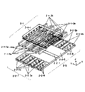
[Fig. 1] Fig. 1 is an exploded perspective view of a high-
frequency line connecting structure according to a first
embodiment of the present invention.
[Fig. 2] Fig. 2 is an exploded perspective view of the
high-frequency line connecting structure according to the first
embodiment of the present invention.
[Fig. 3] Fig. 3 is a bottom view of the high-frequency
line connecting structure according to the first embodiment of the
present invention.
[Fig. 4] Fig. 4 is a perspective view of a high-frequency
line connecting structure according to the first embodiment of the
present invention.
[Fig. 5] Fig. 5 is a plan view of the high-frequency line
connecting structure according to the first embodiment of the
present invention.
11
CA 03158938 2022-04-25
[Fig. 6] Fig. 6 is a side view of the high-frequency line
connecting structure according to the first embodiment of the
present invention.
[Fig. 7] Fig. 7 is a diagram illustrating simulation
results of reflection loss characteristics and passage loss
characteristics of the high-frequency line connecting structure
according to the first embodiment of the present invention.
[Fig. 8] Fig. 8 is a diagram illustrating simulation
results of crosstalk characteristics between adjacent channels and
passage loss characteristics of the high-frequency line connecting
structure according to the first embodiment of the present
invention.
[Fig. 9] Fig. 9 is an exploded perspective view of a high-
frequency line connecting structure according to a second
embodiment of the present invention.
[Fig. 10] Fig. 10 is an exploded perspective view of the
high-frequency line connecting structure according to the second
embodiment of the present invention.
[Fig. 11] Fig. 11 is a bottom view of a high-frequency
line substrate of the high-frequency line connecting structure
according to the second embodiment of the present invention.
[Fig. 12] Fig. 12 is a plan view of the high-frequency
line substrate of the high-frequency line connecting structure
according to the second embodiment of the present invention.
[Fig. 13] Fig. 13 is a perspective view of the high-
frequency line connecting structure according to the second
embodiment of the present invention.
12
CA 03158938 2022-04-25
[Fig. 14] Fig. 14 is a plan view of the high-frequency
line connecting structure according to the second embodiment of
the present invention.
[Fig. 15] Fig. 15 is a side view of the high-frequency
line connecting structure according to the second embodiment of
the present invention.
[Fig. 16] Fig. 16 is a diagram illustrating simulation
results of reflection loss characteristics and passage loss
characteristics of the high-frequency line connecting structure
according to the second embodiment of the present invention.
[Fig. 17] Fig. 17 is a diagram illustrating simulation
results of crosstalk characteristics between adjacent channels and
passage loss characteristics of the high-frequency line connecting
structure according to the second embodiment of the present
invention.
[Fig. 18A] Fig. 18A is a plan view of a multilayer printed
circuit board of the prior art.
[Fig. 18B] Fig. 18B is a cross-sectional view of the
multilayer printed circuit board of the prior art.
[Fig. 19] Fig. 19 is a diagram illustrating reflection
loss characteristics and passage loss characteristics of the
multilayer printed circuit board of the prior art.
Description of Embodiments
[0023] Embodiments of the present invention are described
hereinafter in detail with reference to the drawings.
[0024] [First Embodiment]
13
CA 03158938 2022-04-25
,
..
Fig. 1 is an exploded perspective view showing, from
above, a high-frequency line connecting structure according to a
first embodiment of the present invention, and Fig. 2 is an
exploded perspective view showing the high-frequency line
connecting structure from below. As shown in Figs. 1 and 2, a
printed circuit board 2-2 (first substrate) includes a flat plate-
shaped dielectric 2-2-5, a microstrip line 2-2-1 made of a
conductor that is formed on an upper surface (first main surface)
of the dielectric 2-2-5, signal lines 2-2-3a and 2-2-3b (first
signal lines) made of conductors that are formed on the upper
surface of the dielectric 2-2-5 along a direction intersecting
with the microstrip lines 2-2-1, ground planes 2-2-2a and 2-2-2b
(first grounds) made of conductors that are formed on the upper
surface of the dielectric 2-2-5 along the signal lines 2-2-3a and
2-2-3b, a ground plane 2-2-4 made of a conductor that is formed on
a lower surface (second main surface) of the dielectric 2-2-5, and
ground vias 2-2-6 made of conductors that connect the ground
planes 2-2-2a and 2-2-2b to the ground plane 2-2-4.
[0025] In the present embodiment, a plurality of the signal lines
2-2-3a are arranged in parallel. A plurality of the ground planes
2-2-2a are arranged on both sides of the signal lines 2-2-3a along
the signal lines 2-2-3a. Similarly, a plurality of the signal
lines 2-2-3b are arranged in parallel. A plurality of the ground
planes 2-2-2b are arranged on both sides of the signal lines 2-2-
3b along the signal lines 2-2-3b.
[0026] The signal lines 2-2-3a and the signal lines 2-2-3b are
divided at the intersections thereof with the microstrip line 2-2-
14
CA 03158938 2022-04-25
1. Similarly, the ground planes 2-2-2a and the ground planes 2-2-
2b are divided at sections which are at the same position in
extension direction (X direction in Figs. 1 and 2) as the sections
where the signal lines 2-2-3a and 2-2-3b are divided.
[0027] The ground planes 2-2-2a and 2-2-2b are electrically
connected to the ground plane 2-2-4 by the ground vias 2-2-6
formed on the dielectric 2-2-5.
[0028] The signal lines 2-2-3a and 2-2-3b and the ground planes
2-2-2a and 2-2-2b constitute a grounded coplanar line 2-2-7 (first
high-frequency line) having the ground plane 2-2-4 on a rear
surface of the substrate. As described above, the grounded
coplanar line 2-2-7 is divided at the intersection thereof with
the microstrip line 2-2-1.
[0029] Next is described a high-frequency line substrate 2-1
(second substrate) for connecting the divided grounded coplanar
lines 2-2-7 located on both sides of the microstrip line 2-2-1.
Fig. 3 is a bottom view of the high-frequency line substrate 2-1.
In Fig. 3, the descriptions of the signal lead pins and the ground
lead pins, which will be described later, are omitted in order to
facilitate understanding of the configuration of the high-
frequency line substrate 2-1.
[0030] As shown in Figs. 1 to 3, the high-frequency line
substrate 2-1 includes a flat plate-shaped dielectric 2-1-1, a
ground plane 2-1-4 made of a conductor that is formed on a lower
surface of the dielectric 2-1-1 facing the printed circuit board
2-2, a dielectric 2-1-7 formed on a lower surface of the ground
plane 2-1-4 facing the printed circuit board 2-2, a signal line 2-
CA 03158938 2022-04-25
1-6 (second signal line) made of a conductor that is formed on a
lower surface (first main surface) of the dielectric 2-1-7 facing
the printed circuit board 2-2, so that the extension direction
becomes parallel to the extension direction of the signal lines 2-
2-3a and 2-2-3b when the high-frequency line substrate 2-1 is
mounted on the printed circuit board 2-2, and a ground plane 2-1-5
(second ground) made of a conductor that is formed on the lower
surface of the dielectric 2-1-7 facing the printed circuit board
2-2, along the signal line 2-1-6, so that the extension direction
becomes parallel to the extension direction of the ground planes
2-2-2a and 2-2-2b when the high-frequency line substrate 2-1 is
mounted on the printed circuit board 2-2.
[0031] The high-frequency line substrate 2-1 further includes
signal lead pins 2-1-3a and 2-1-3b made of conductors that are
connected to both ends of the signal line 2-1-6 respectively so as
to be in contact with the signal lines 2-2-3a and 2-2-3b when the
high-frequency line substrate 2-1 is mounted on the printed
circuit board 2-2, ground lead pins 2-1-2a and 2-1-2b made of
conductors that are connected to both ends of the ground plane 2-
1-5 respectively so as to be in contact with the ground planes 2-
2-2a and 2-2-2b when the high-frequency line substrate 2-1 is
mounted on the printed circuit board 2-2, and ground vias 2-1-8
made of conductors that are formed in the dielectric 2-1-7 and
connect the ground plane 2-1-4 and the ground plane 2-1-5.
[0032] Examples of the material of the dielectrics 2-1-1, 2-1-7,
and 2-2-5 include low-loss ceramics such as alumina.
16
CA 03158938 2022-04-25
In the present embodiment, a plurality of the signal lines
2-1-6 are arranged in parallel on the lower surface of the high-
frequency line substrate 2-1. The pitch of the signal lines 2-1-6
in the alignment direction (Y direction in Figs. 1 to 3) is the
same as the pitch of the signal lines 2-2-3a and 2-2-3b in the
alignment direction.
[0033] A plurality of the ground planes 2-1-5 are arranged on
both sides of the signal lines 2-1-6 along the signal lines 2-1-6.
The pitch of the ground planes 2-1-5 in the alignment direction is
the same as the pitch of the ground planes 2-2-2a and 2-2-2b in
the alignment direction.
[0034] The ground planes 2-1-5 are electrically connected to the
ground planes 2-1-4 by the ground vias 2-1-8 formed on the
dielectric 2-1-7.
The signal lines 2-1-6 and the ground planes 2-1-5
constitute a grounded coplanar line 2-1-9 (second high-frequency
line) having the ground plane 2-1-4 on the opposite side with the
dielectric 2-1-7 therebetween.
[0035] In the present embodiment, a plurality of the signal lead
pins 2-1-3a and 2-1-3b are arranged in parallel along the
alignment direction of the signal lines 2-2-3a and 2-2-3b and the
alignment direction (Y direction in Figs. 1 to 3) of the signal
lines 2-1-6. The pitch of the signal lead pins 2-1-3a and 2-1-3b
in the alignment direction is the same as the pitch of the signal
lines 2-2-3a and 2-2-3b and the signal lines 2-1-6 in the
alignment direction.
17
CA 03158938 2022-04-25
[0036] A plurality of the ground lead pins 2-1-2a and 2-1-2b are
arranged in parallel along the alignment direction of the ground
planes 2-2-2a and 2-2-2b and the alignment direction (Y direction
in Figs. 1 to 3) of the ground planes 2-1-5. The pitch of the
ground lead pins 2-1-2a and 2-1-2b in the alignment direction is
the same as the pitch of the ground planes 2-2-2a and 2-2-2b and
the ground planes 2-1-5 in the alignment direction.
[0037] Examples of a method for fixing the signal lead pins 2-1-
3a and 2-1-3b to the signal lines 2-1-6 and a method for fixing
the ground lead pins 2-1-2a and 2-1-2b to the ground planes 2-1-5
include brazing and soldering; needless to say, other fixing
methods may be adopted.
[0038] After the high-frequency line substrate 2-1 and the
printed circuit board 2-2 described above are individually
prepared, the high-frequency line substrate 2-1 is mounted on the
printed circuit board 2-2.
Fig. 4 is a perspective view of a high-frequency line
connecting structure in which the high-frequency line substrate 2-
1 is mounted on the printed circuit board 2-2, and the divided
grounded coplanar lines 2-2-7 of the printed circuit board 2-2 are
connected by the grounded coplanar line 2-1-9 of the high-
frequency line substrate 2-1. Fig. 5 is a plan view of the high-
frequency line connecting structure of Fig. 4, and Fig. 6 is a
side view of the high-frequency line connecting structure of Fig.
4.
[0039] In order to prepare the high-frequency line connecting
structure shown in Figs. 4 to 6, the surface of the high-frequency
18
CA 03158938 2022-04-25
line substrate 2-1 on which the signal lines 2-1-6 and the ground
planes 2-1-5 are formed is placed face-down so the signal lines 2-
1-6 are positioned above the divided sections of the signal lines
2-2-3a and 2-2-3b and the ground planes 2-1-5 are positioned on
the divided sections of the ground planes 2-2-2a and 2-2-2b, and
then the high-frequency line substrate 2-1 is mounted on the
printed circuit board 2-2.
[0040] In so doing, the high-frequency line substrate 2-1 is
mounted on the printed circuit board 2-2 in such a manner that the
signal lead pins 2-1-3a and 2-1-3b of the high-frequency line
substrate 2-1 and the signal lines 2-2-3a and 2-2-3b of the
printed circuit board 2-2 come into contact with each other, and
that the ground lead pins 2-1-2a and 2-1-2b of the high-frequency
line substrate 2-1 and the ground planes 2-2-2a and 2-2-2b of the
printed circuit board 2-2 come into contact with each other.
[0041] The signal lead pins 2-1-3a and 2-1-3b of the high-
frequency line substrate 2-1 and the signal lines 2-2-3a and 2-2-
3b of the printed circuit board 2-2 are connected by soldering or
the like. Similarly, the ground lead pins 2-1-2a and 2-1-2b of the
high-frequency line substrate 2-1 and the ground planes 2-2-2a and
2-2-2b of the printed circuit board 2-2 are connected by soldering
or the like.
[0042] With the high-frequency line connecting structure
described above, the signal line 2-2-3a of the printed circuit
board 2-2 is electrically connected to the signal line 2-2-3b via
the signal lead pin 2-1-3a, the signal line 2-1-6, and the signal
lead pin 2-1-3b of the high-frequency line substrate 2-1.
19
CA 03158938 2022-04-25
Similarly, the ground plane 2-2-2a of the printed circuit board 2-
2 is electrically connected to the ground plane 2-2-2b via the
ground lead pin 2-1-2a, the ground plane 2-1-5, and the ground
lead pin 2-1-2b of the high-frequency line substrate 2-1. In the
present embodiment, the microstrip line 2-2-1 and the grounded
coplanar line 2-2-7 formed on the upper surface of the printed
circuit board 2-2 can be crossed three-dimensionally.
[0043] In
the present embodiment, as shown in Fig. 6, the shapes
of the ground lead pins 2-1-2a and 2-1-2b and of the signal lead
pins 2-1-3a and 2-1-3b are determined in such a manner that the
height of the ground lead pins 2-1-2a and 2-1-2b from the upper
surface of the printed circuit board 2-2 is greater than that of
the signal lead pins 2-1-3a and 2-1-3b at the contact portions
between the signal lead pins 2-1-3a and 2-1-3b and the signal
lines 2-2-3a and 2-2-3b, and the contact portions between the
ground lead pins 2-1-2a and 2-1-2b and the ground planes 2-2-2a
and 2-2-2b.
[0044] As is clear from Fig. 6, needless to say, the height of
upper surfaces of the signal lead pins 2-1-3a and 2-1-3b at the
connection portions between the signal lead pins 2-1-3a and 2-1-3b
and the signal lines 2-1-6 is the same as the height of the upper
surfaces of the ground lead pins 2-1-2a and 2-1-2b at the
connection portions between the ground lead pins 2-1-2a and 2-1-2b
and the ground planes 2-1-5. The signal lead pins 2-1-3a and 2-1-
3b are shaped such that the upper surfaces thereof become lower in
height from the high-frequency line substrate 2-1 toward the
signal lines 2-2-3a and 2-2-3b, respectively.
CA 03158938 2022-04-25
[0045] A high-frequency signal propagates from the printed
circuit board 2-2 to the high-frequency line substrate 2-1 through
the signal lead pin 2-1-3a. Furthermore, a high-frequency signal
propagates from the high-frequency line substrate 2-1 to the
printed circuit board 2-2 through the signal lead pin 2-1-3b. In
such a case, since the signal lead pins 2-1-3a and 2-1-3b are
exposed to the air, the capacitance between the signal lead pins
2-1-3a and 2-1-3b and the ground lead pins 2-1-2a and 2-1-2b
decreases, and the characteristic impedance of the coplanar line
tends to increase.
[0046] In the present embodiment, at the contact portions between
the signal lead pins 2-1-3a and 2-1-3b and the signal lines 2-2-3a
and 2-2-3b, and the contact portions between the ground lead pins
2-1-2a and 2-1-2b and the ground planes 2-2-2a and 2-2-2b, the
height of the ground lead pins 2-1-2a and 2-1-2b is made greater
than that of the signal lead pins 2-1-3a and 2-1-3b. Thus, a
structure is obtained in which the signal lead pins 2-1-3a and 2-
1-3b are surrounded by the ground lead pins 2-1-2a and 2-1-2b that
each function as the ground of the coplanar line.
[0047] With this structure, in the present embodiment, not only
is it possible to prevent a decrease in capacitance between the
signal lead pins 2-1-3a and 2-1-3b and the ground lead pins 2-1-2a
and 2-1-2b, but also an increase in the characteristic impedance
of the coplanar lines can be suppressed. As a result, impedance
matching can be achieved between the grounded coplanar line 2-2-7
of the printed circuit board 2-2 and the grounded coplanar line 2-
1-9 of the high-frequency line substrate 2-1.
21
CA 03158938 2022-04-25
[0048] In addition, in the present embodiment, the ground lead
pins 2-1-2a and 2-1-2b can enclose a line of electric force from
the signal lead pins 2-1-3a and 2-1-3b so as not to leak the line
of electric force to the adjacent signal lead pins 2-1-3a and 2-1-
3b. As a result, crosstalk between the signal lead pins 2-1-3a and
2-1-3b and the adjacent signal lead pins 2-1-3a and 2-1-3b can be
reduced.
[0049] Fig. 7 is a diagram illustrating simulation results of
reflection loss characteristics and passage loss characteristics
of the grounded coplanar line in the high-frequency line
connecting structure of the present embodiment. Fig. 8 is a
diagram illustrating simulation results of crosstalk
characteristics between adjacent channels and passage loss
characteristics of the grounded coplanar line in the high-
frequency line connecting structure of the present embodiment.
[0050] Reference numeral 700 in Figs. 7 and 8 indicates the
reflection loss characteristics, and reference numeral 701
indicates the passage loss characteristics. Reference numeral 702
of Fig. 8 indicates a crosstalk between adjacent channels
occurring when the shape of the ground lead pins 2-1-2a and 2-1-2b
is identical to that of the signal lead pins 2-1-3a and 2-1-3b,
and reference numeral 703 indicates a crosstalk between adjacent
channels in the present embodiment.
[0051] In the present embodiment, by mounting the high-frequency
line substrate 2-1 on the printed circuit board 2-2, the grounded
coplanar lines 2-2-7 divided at the intersection thereof with the
microstrip line 2-2-1 are connected via the high-frequency line
22
CA 03158938 2022-04-25
A
substrate 2-1. Also in the present embodiment, by making the
height of the ground lead pins 2-1-2a and 2-1-2b at the connection
portion with the printed circuit board 2-2 greater than that of
the signal lead pins 2-1-3a and 2-1-3b, impedance matching can be
achieved between the grounded coplanar line 2-2-7 of the printed
circuit board 2-2 and the grounded coplanar line 2-1-9 of the
high-frequency line substrate 2-1.
[0052] As a result, in the present embodiment, the high-frequency
line connecting structure capable of achieving favorable effects
as shown in Figs. 7 and 8 and realizing low reflection loss
characteristics, low passage loss characteristics, and low
crosstalk characteristics in a wide band, can be obtained.
[0053] [Second Embodiment]
A second embodiment of the present invention is described
next. Fig. 9 is an exploded perspective view showing, from above,
a high-frequency line connecting structure according to the second
embodiment of the present invention. Fig. 10 is an exploded
perspective view showing the high-frequency line connecting
structure of Fig. 9 from below. Fig. 11 is a bottom view of the
high-frequency line substrate. Fig. 12 is a plan view of the high-
frequency line substrate. Note that, in Fig. 11, the descriptions
of the signal lead pins and the ground lead pins are omitted in
order to facilitate understanding of the configuration of the
high-frequency line substrate. Also in Fig. 12, the description of
the DC block capacitor is omitted in order to facilitate
understanding of the configuration of the high-frequency line
substrate.
23
CA 03158938 2022-04-25
N
,
[0054] Fig. 13 is a perspective view of the high-frequency line
connecting structure in which a high-frequency line substrate is
mounted on a printed circuit board, and a grounded coplanar line
of the printed circuit board is connected by a grounded coplanar
line of the high-frequency line substrate. Fig. 14 is a plan view
of the high-frequency line connecting structure of Fig. 13, and
Fig. 15 is a side view of the high-frequency line connecting
structure of Fig. 13.
[0055] A printed circuit board 3-2 (first substrate) of the
present embodiment includes a flat plate-shaped dielectric 3-2-5,
signal lines 3-2-3a and 3-2-3b (first signal lines) made of
conductors that are formed on an upper surface (first main
surface) of the dielectric 3-2-5, ground planes 3-2-2a and 3-2-2b
(first grounds) made of conductors that are formed on the upper
surface of the dielectric 3-2-5 along the signal lines 3-2-3a and
3-2-3b, a ground plane 3-2-4 made of a conductor that is formed on
a lower surface (second main surface) of the dielectric 3-2-5, and
ground vias 3-2-6 made of conductors that connect the ground
planes 3-2-2a and 3-2-2b to the ground plane 3-2-4.
[0056] In the present embodiment, a plurality of the signal lines
3-2-3a are arranged in parallel. A plurality of the ground planes
3-2-2a are arranged on both sides of the signal lines 3-2-3a along
the signal lines 3-2-3a. Similarly, a plurality of the signal
lines 3-2-3b are arranged in parallel. A plurality of ground
planes 3-2-2b are arranged on both sides of the signal lines 3-2-
3b along the signal lines 3-2-3b.
24
CA 03158938 2022-04-25
[0057] The signal lines 3-2-3a and the signal lines 3-2-3b are
divided at the position where a DC block capacitor is mounted as
described hereinafter. Similarly, the ground planes 3-2-2a and the
ground planes 3-2-2b are divided at sections which are at the same
position in the extension direction (X direction in Figs. 9 to 15)
as the sections where the signal lines 3-2-3a and 3-2-3b are
divided.
[0058] The ground planes 3-2-2a and 3-2-2b are electrically
connected to the ground plane 3-2-4 by the ground vias 3-2-6
formed on the dielectric 3-2-5.
[0059] The signal lines 3-2-3a and 3-2-3b and the ground planes
3-2-2a and 3-2-2b constitute a grounded coplanar line 3-2-7 (first
high-frequency line) having the ground plane 3-2-4 on a rear
surface of the substrate. The grounded coplanar line 3-2-7 is
divided at a section where the high-frequency line substrate is
mounted, in order to insert the DC block capacitor in series as
described hereinafter.
[0060] On the other hand, the high-frequency line substrate 3-1
(second substrate) includes a flat plate-shaped dielectric 3-1-1,
signal lines 3-1-6a and 3-1-6b (second signal lines) made of
conductors that are formed on a lower surface (first main surface)
of the dielectric 3-1-1 facing the printed circuit board 3-2 so
that the extension direction becomes parallel to the extension
direction of the signal lines 3-2-3a and 3-2-3b when the high-
frequency line substrate 3-1 is mounted on the printed circuit
board 3-2, a ground plane 3-1-5 (second ground) made of a
conductor that is formed on the lower surface of the dielectric 3-
CA 03158938 2022-04-25
1-1 facing he printed circuit board 3-2 so as to surround the
signal line 3-1-6a and 3-1-6b, signal lines 3-1-7a and 3-1-7b
(third signal lines) made of conductors that are formed on an
upper surface (second main surface) of the dielectric 3-1-1, and a
ground plane 3-1-4 (third ground) formed on the upper surface of
the dielectric 3-1-1 so as to surround the signal lines 3-1-7a and
3-1-7b.
[0061] The high-frequency line substrate 3-1 further includes
signal lead pins 3-1-3a and 3-1-3b made of conductors that are
connected to the signal lines 3-1-6a and 3-1-6b respectively so as
to be in contact with the signal lines 3-2-3a and 3-2-3b when the
high-frequency line substrate 3-1 is mounted on the printed
circuit board 3-2, ground lead pins 3-1-2a and 3-1-2b made of
conductors that are connected to both ends of the ground plane 2-
1-5 respectively so as to be in contact with the ground planes 3-
2-2a and 3-2-2b when the high-frequency line substrate 3-1 is
mounted on the printed circuit board 3-2, ground vias 3-1-8 made
of conductors that are formed on the dielectric 3-1-1 and connect
the ground plane 3-1-4 and the ground plane 3-1-5 to each other,
vias 3-1-9a and 3-1-9b made of conductors that are formed on the
dielectric 3-1-1 and connect the signal lines 3-1-6a and 3-1-6b
and the signal lines 3-1-7a and 3-1-7b to each other, and a DC
block capacitor 3-1-10 (electronic component).
[0062] Examples of the material of the dielectrics 3-1-1 and 3-2-
include low-loss ceramics such as alumina.
In the present embodiment, a plurality of the signal lines
3-1-6a are arranged in parallel on the lower surface of the high-
26
CA 03158938 2022-04-25
,
,
,
frequency line substrate 3-1. Similarly, a plurality of the signal
lines 3-1-6b are arranged in parallel. The ground planes 3-1-5 are
arranged so as to surround the signal lines 3-1-6a and 3-1-6b. The
signal lines 3-1-6a and the signal lines 3-1-6b are divided in
order to mount the DC block capacitor 3-1-10 on the opposite
surface. The pitch of the signal lines 3-1-6a and 3-1-6b in the
alignment direction (Y direction in FIGS. 9 to 15) is the same as
the pitch of the signal lines 3-2-3a and 3-2-3b in the alignment
direction.
[0063] In the present embodiment, a plurality of the signal lines
3-1-7a are arranged in parallel on the upper surface of the high-
frequency line substrate 3-1. Similarly, a plurality of the signal
lines 3-1-7b are arranged in parallel. The ground planes 3-1-4 are
arranged so as to surround the signal lines 3-1-7a and 3-1-7b. The
signal lines 3-1-7a and the signal lines 3-1-7b are divided in
order to mount the DC block capacitor 3-1-10 on the upper surface
of the high-frequency line substrate 3-1. The pitch of the signal
lines 3-1-7a and 3-1-7b in the alignment direction (Y direction in
Figs. 9 to 15) is the same as the pitch of the signal lines 3-1-6a
and 3-1-6b in the alignment direction.
[0064] The ground planes 3-1-5 are electrically connected to the
ground planes 3-1-4 by the ground vias 3-1-8 formed on the
dielectric 3-1-1.
Ends of the signal lines 3-1-7a are electrically connected
to one of the two parts of the second signal line (signal line 3-
1-6a) via the via 3-1-9a formed in the dielectric 3-1-1. Ends of
the signal lines 3-1-7b are electrically connected to the other
27
CA 03158938 2022-04-25
one of the two parts of the second signal line (signal line 3-1-
6b) via the vias 3-1-9b formed in the dielectric 3-1-1.
[0065] The ground planes 3-1-5 are formed around the signal lines
3-1-6a and 3-1-6b, and the ground planes 3-1-4 are formed around
the signal lines 3-1-7a and 3-1-7b. Thus, the signal lines 3-1-6a
and 3-1-7a, the vias 3-1-9a, and the ground planes 3-1-4 and 3-1-5
constitute a pseudo-coaxial line structure 3-1-13a formed along a
vertical direction of the high-frequency line substrate 3-1
(dielectric 3-1-1). Similarly, the signal lines 3-1-6b and 3-1-7b,
the vias 3-1-9b, and the ground planes 3-1-4 and 3-1-5 constitute
a pseudo-coaxial line structure 3-1-13b.
[0066] The signal lines 3-1-6a and 3-1-6b and the ground planes
3-1-5 constitute a grounded coplanar line 3-1-11 (second high-
frequency line) having the ground planes 3-1-4 on the opposite
side with the dielectric 3-1-1 therebetween. The grounded coplanar
line 3-1-11 is divided into two in order to insert the DC block
capacitor 3-1-10 in series.
[0067] The signal lines 3-1-7a and 3-1-7b and the ground plane 3-
1-4 constitute a grounded coplanar line 3-1-12 (third high-
frequency line) having the ground plane 3-1-5 on the opposite side
with the dielectric 3-1-1 therebetween. The grounded coplanar line
3-1-12 is divided into two in order to insert the DC block
capacitor 3-1-10 in series.
[0068] One electrode of the DC block capacitor 3-1-10 is soldered
to one of the two divided sections of the third signal line
(signal line 3-1-7a). The other electrode of the DC block
capacitor 3-1-10 is soldered to the other part (signal line 3-1-
28
CA 03158938 2022-04-25
A
7b) of the two divided sections of the third signal line. In this
manner, the DC block capacitor 3-1-10 is mounted on the high-
frequency line substrate 3-1 and the DC block capacitor 3-1-10 is
inserted in series into the grounded coplanar lines 3-1-11 and 3-
1-12.
[0069] Examples of a method for fixing the signal lead pins 3-1-
3a and 3-1-3b to the signal lines 3-1-6a and 3-1-6b and a method
for fixing the ground lead pins 3-1-2a and 3-1-2b to the ground
planes 3-1-5 include brazing and soldering; needless to say, other
fixing methods may be adopted.
[0070] After the high-frequency line substrate 3-1 and the
printed circuit board 3-2 described above are individually
prepared, the high-frequency line substrate 3-1 is mounted on the
printed circuit board 3-2.
In order to prepare the high-frequency line connecting
structure shown in Figs. 13 to 15, the surface of the high-
frequency line substrate 3-1 on which the signal lines 3-1-6a and
3-1-6b and the ground planes 3-1-5 are formed is placed face-down
so the signal lines 3-1-6a, 3-1-6b, 3-1-7a, and 3-1-7b are
positioned above the divided section of the signal lines 3-2-3a
and 3-2-3b and the ground planes 3-1-5 and 3-1-4 are positioned on
the divided section of the ground planes 3-2-2a and 3-2-2b, and
then the high-frequency line substrate 3-1 is mounted on the
printed circuit board 3-2.
[0071] In so doing, the high-frequency line substrate 3-1 is
mounted on the printed circuit board 3-2 in such a manner that the
signal lead pins 3-1-3a and 3-1-3b of the high-frequency line
29
CA 03158938 2022-04-25
substrate 3-1 and the signal lines 3-2-3a and 3-2-3b of the
printed circuit board 3-2 come into contact with each other, and
that the ground lead pins 3-1-2a and 3-1-2b of the high-frequency
line substrate 3-1 and the ground planes 3-2-2a and 3-2-2b of the
printed circuit board 3-2 come into contact with each other.
[0072] The signal lead pins 3-1-3a and 3-1-3b of the high-
frequency line substrate 3-1 and the signal lines 3-2-3a and 3-2-
3b of the printed circuit board 3-2 are connected by soldering or
the like. Similarly, the ground lead pins 3-1-2a and 3-1-2b of the
high-frequency line substrate 3-1 and the ground planes 3-2-2a and
3-2-2b of the printed circuit board 3-2 are connected by soldering
or the like.
[0073] With the high-frequency line connecting structure
described above, the signal line 3-2-3a of the printed circuit
board 3-2 is electrically connected to the signal line 3-2-3b via
the signal lead pin 3-1-3a, the signal line 3-1-6a, the via 3-1-
9a, the signal line 3-1-7a, the DC block capacitor 3-1-10, the
signal line 3-1-7b, the via 3-1-9b, the signal line 3-1-6b and the
signal lead pin 3-1-3b of the high-frequency line substrate 3-1.
[0074] The ground plane 3-2-2a of the printed circuit board 3-2
is electrically connected to the ground plane 3-2-2b via the
ground lead pin 3-1-2a, the ground plane 3-1-5, and the ground
lead pin 3-1-2b of the high-frequency line substrate 3-1.
In this manner, the high-frequency line substrate 3-1 on
which the DC block capacitor 3-1-10 is mounted can be mounted on
the printed circuit board 3-2, whereby the DC block capacitor 3-1-
CA 03158938 2022-04-25
.'
.'
can be inserted in series into the grounded coplanar lines 3-2-
7.
[0075]
In the present embodiment, as shown in Fig. 15, the shapes
of the ground lead pins 3-1-2a and 3-1-2b and of the signal lead
pins 3-1-3a and 3-1-3b are determined in such a manner that the
height of the ground lead pins 3-1-2a and 3-1-2b from the upper
surface of the printed circuit board 3-2 is greater than that of
the signal lead pins 3-1-3a and 3-1-3b at the contact portions
between the signal lead pins 3-1-3a and 3-1-3b and the signal
lines 3-2-3a and 3-2-3b, and the contact portions between the
ground lead pins 3-1-2a and 3-1-2b and the ground planes 3-2-2a
and 3-2-2b.
[0076] As is clear from Fig. 15, needless to say, the height of
upper surfaces of the signal lead pins 3-1-3a and 3-1-3b at the
connection portions between the signal lead pins 3-1-3a and 3-1-3b
and the signal lines 3-1-6a and 3-1-6b is the same as the height
of the upper surfaces of the ground lead pins 3-1-2a and 3-1-2b at
the connection portions between the ground lead pins 3-1-2a and 3-
1-2b and the ground planes 3-1-5. The signal lead pins 3-1-3a and
3-1-3b are shaped such that the upper surfaces thereof become
lower in height from the high-frequency line substrate 3-1 toward
the signal lines 3-2-3a and 3-2-3b.
[0077] A high-frequency signal propagates from the printed
circuit board 3-2 to the high-frequency line substrate 3-1 through
the signal lead pin 3-1-3a. Furthermore, a high-frequency signal
propagates from the high-frequency line substrate 3-1 to the
printed circuit board 3-2 through the signal lead pin 3-1-3b. In
31
CA 03158938 2022-04-25
1
such a case, since the signal lead pins 3-1-3a and 3-1-3b are
exposed to the air, the capacitance between the signal lead pins
3-1-3a and 3-1-3b and the ground lead pins 3-1-2a and 3-1-2b
decreases, and the characteristic impedance of the coplanar line
tends to increase.
[0078] In the present embodiment, at the contact portions between
the signal lead pins 3-1-3a and 3-1-3b and the signal lines 3-2-3a
and 3-2-3b, and the contact portions between the ground lead pins
3-1-2a and 3-1-2b and the ground planes 3-2-2a and 3-2-2b, the
height of the ground lead pins 3-1-2a and 3-1-2b is made greater
than that of the signal lead pins 3-1-3a and 3-1-3b. Thus, a
structure is obtained in which the signal lead pins 3-1-3a and 3-
1-3b are surrounded by the ground lead pins 3-1-2a and 3-1-2b that
each function as the ground of the coplanar line.
[0079] With this structure, in the present embodiment, not only
is it possible to prevent a decrease in capacitance between the
signal lead pins 3-1-3a and 3-1-3b and the ground lead pins 3-1-2a
and 3-1-2b, but also an increase in the characteristic impedance
of the coplanar lines can be suppressed. As a result, impedance
matching can be achieved between the grounded coplanar line 3-2-7
of the printed circuit board 3-2 and the grounded coplanar lines
3-1-11 and 3-1-12 of the high-frequency line substrate 3-1.
[0080] In addition, in the present embodiment, the ground lead
pins 3-1-2a and 3-1-2b can enclose a line of electric force from
the signal lead pins 3-1-3a and 3-1-3b so as not to leak the line
of electric force to the adjacent signal lead pins 3-1-3a and 3-1-
3b. As a result, crosstalk between the signal lead pins 3-1-3a and
32
CA 03158938 2022-04-25
3-1-3b and the adjacent signal lead pins 3-1-3a and 3-1-3b can be
reduced.
[0081] Fig. 16 is a diagram illustrating simulation results of
reflection loss characteristics and passage loss characteristics
of the grounded coplanar line in the high-frequency line
connecting structure of the present embodiment, and Fig. 17 is a
diagram showing simulation results of crosstalk characteristics
between adjacent channels and passage loss characteristics of the
grounded coplanar line in the high-frequency line connecting
structure of the present embodiment.
[0082] Reference numeral 600 in Figs. 16 and 17 indicates the
reflection loss characteristics, and reference numeral 601
indicates the passage loss characteristics. Reference numeral 602
of Fig. 17 indicates a crosstalk between adjacent channels
occurring when the shape of the ground lead pins 3-1-2a and 3-1-2b
is identical to that of the signal lead pins 3-1-3a and 3-1-3b,
and reference numeral 603 indicates a crosstalk between adjacent
channels in the present embodiment.
[0083] In the present embodiment, by mounting the high-frequency
line substrate 3-1 onto the printed circuit board 3-2, the DC
block capacitor 3-1-10 is inserted in series into the grounded
coplanar line 3-2-7. Also in the present embodiment, by making the
ground lead pins 3-1-2a and 3-1-2b at the connection portion with
the printed circuit board 3-2 higher than the signal lead pins 3-
1-3a and 3-1-3b, impedance matching can be achieved between the
grounded coplanar line 3-2-7 of the printed circuit board 3-2 and
33
CA 03158938 2022-04-25
the grounded coplanar lines 3-1-11 and 3-1-12 of the high-
frequency line substrate 3-1.
[0084] As a result, in the present embodiment, the high-frequency
line connecting structure capable of achieving favorable effects
as shown in Figs. 16 and 17 and realizing low reflection loss
characteristics, low passage loss characteristics, and low
crosstalk characteristics in a wide bandwidth, can be obtained.
[0085] Note that, in the present embodiment, the DC block
capacitor is described as an example of the electronic component
to be inserted in series into the coplanar line, but an electronic
component other than the DC block capacitor may be used.
[0086] In
the first and second embodiments, the dielectric 2-1-1,
2-1-7, 2-2-5, 3-1-1, and 3-2-5 constituting the grounded coplanar
lines 2-1-9, 2-2-7, 3-1-11, 3-1-12, and 3-2-7 are low-loss
ceramics such as alumina, but needless to say, liquid crystal
polymer, polymide, quartz glass, or the like can be used instead.
[0087] Also, in the first and second embodiments, when mounting
the high-frequency line substrates 2-1 and 3-1 on the printed
circuit boards 2-2 and 3-2, the connection portions between the
signal lead pins 2-1-3a, 2-1-3b, 3-1-3a, and 3-1-3b and the signal
lines 2-2-3a, 2-2-3b, 3-2-3a, and 3-2-3b, the connection portions
between the ground lead pins 2-1-2a, 2-1-2b, 3-1-2a, and 3-1-2b
and the ground planes 2-2-2a, 2-2-2b, 3-2-2a, and 3-2-2b, the
connection portions between the signal lead pins 2-1-3a, 2-1-3b,
3-1-3a, and 3-1-3b and the signal lines 2-1-6, 3-1-6a, and 3-1-6b,
and the connection portions between the ground lead pins 2-1-2a,
2-1-2b, 3-1-2a, and 3-1-2b and the ground planes 2-1-5 and 3-1-5
34
CA 03158938 2022-04-25
are typically gold-plated for the purpose of improving solder
wettability. However, gold plating is not specified in particular
because it is not the essence of the present invention.
Industrial Applicability
[0088] The present invention can be applied to a technique for
three-dimensionally crossing high-frequency lines of a printed
circuit board and inserting electronic components into the high-
frequency lines of the printed circuit board.
Reference Signs List
[0089] 2-1, 3-1 High-frequency line substrate
2-1-1, 2-2-5, 3-1-1, 3-2-5 Dielectric
2-1-2a, 2-1-2b, 3-1-2a, 3-1-2b Ground lead pin
2-1-3a, 2-1-3b, 3-1-3a, 3-1-3b Signal lead pin
2-1-4, 2-1-5, 2-2-2a, 2-2-2b, 2-2-4, 3-1-4, 3-1-5, 3-2-2a, 3-2-2b
Ground plane
2-1-6, 2-2-3a, 2-2-3b, 3-1-6a, 3-1-6b, 3-1-7a, 3-1-7b, 3-2-3a, 3-
2-3b Signal line
2-1-7 Dielectric
2-1-8, 2-2-6, 3-2-6, 3-1-8 Ground via
2-1-9, 2-2-7, 3-1-11, 3-1-12, 3-2-7 Grounded coplanar line
2-2, 3-2 Printed circuit board
2-2-1 Microstrip line
3-1-9a, 3-1-9b Via
3-1-10 DC block capacitor
3-1-13a, 3-1-13b Pseudo-coaxial line structure