Note : Les descriptions sont présentées dans la langue officielle dans laquelle elles ont été soumises.
WO 2021/110508
PCT/EP2020/083353
DETUNING DETECTION AND COMPENSATION FOR INDUCTIVE COUPLING
SYSTEMS
PRIORITY APPLICATION
This application claims priority to U. S. Patent Application Serial Number
16/704,252, filed December 5, 2019, the disclosure of which is incorporated
herein in its
entirety by reference.
FIELD OF THE DISCLOSURE
This document pertains generally, but not by way of limitation, to Radio
Frequency
Identification (REID) systems and, more particularly, to techniques for
reducing harmful
interference effects in RF1D systems.
BACKGROUND
An RFID system is a system that uses radio frequency transponders (e.g., tags)
to
identify items-of-interest. Each radio frequency transponder is attached to or
near a
corresponding item and includes information identifying that item. When an
identification
needs to be made, a radio frequency reader unit (e.g., an interrogator) is
used to excite (e.g.,
interrogate) the transponder on the item that then transmits an identification
signal (including
the identification information for the item) back to the reader unit. The
reader unit then uses
the identification information received from the transponder to perform any of
a number of
different RFID applications. For example, the identification information can
be used to
perform fimctions such as asset management, inventory tracking, access
control, and others.
SUMMARY OF THE DISCLOSURE
In some certain embodiments, a system and method are provided for operating an
inductive coupling reader. The disclosed system and method perform operations
comprising'
detecting a change in a resonance frequency of the inductive coupling reader;
comparing the
change in the resonance frequency to a threshold; determining that the change
in the
resonance frequency exceeds the threshold; and activating a compensation
circuit to offset the
change in the resonance frequency of the inductive coupling reader in response
to
determining that the change in the resonance frequency exceeds the threshold.
1
CA 03159892 2022-5-27
WO 2021/110508
PCT/EP2020/083353
In some embodiments, the change in the resonance frequency is caused by an
external
metal material in close proximity to the inductive coupling reader, and a
range of the
inductive coupling reader is reduced as a result of the change in the
resonance frequency.
In some embodiments, detecting the change in the resonance frequency comprises
measuring an amount of current being driven to the inductive coupling reader
using a current
sensor.
In some embodiments, the amount of current being driven to the inductive
coupling
reader is compared to the expected amount of current. In such cases, the
change in the
resonance frequency is determined to exceed the threshold when the amount of
current is less
than the expected amount of current by a given amount.
In some embodiments, the amount of current being driven to the inductive
coupling
reader comprises the current being driven to an antenna of the inductive
coupling reader, and
the given amount comprises ten percent of the expected amount of current.
In some embodiments, the expected amount of current is retrieved from a look-
up
table.
In some embodiments, the compensation circuit comprises one or more capacitors
coupled in parallel to a resonance circuit of the inductive coupling reader.
In some embodiments, proper operation of the inductive coupling reader is
verified
after activating the compensation circuit by comparing a current amount of
current being
driven to the inductive coupling reader to an expected amount of current.
In some embodiments, the threshold comprises a first threshold, and the
compensation
circuit comprises a first compensation circuit. In such cases, the operations
further comprise:
determining that the change in the resonance frequency exceeds the first
threshold and is less
than a second threshold; activating the first compensation circuit in response
to determining
that the change in the resonance frequency exceeds the first threshold and is
less than the
second threshold; determining that the change in the resonance frequency
exceeds the first
threshold and the second threshold; and activating a second compensation
circuit in response
to determining that the change in the resonance frequency exceeds the first
threshold and the
second threshold, wherein the second compensation circuit provides a greater
offset to the
resonance frequency than the first compensation circuit.
In some embodiments, activation of the first compensation circuit couples a
first
capacitor in parallel with a resonance circuit of the inductive coupling
reader, and activation
of the second compensation circuit couples a second capacitor in parallel with
the resonance
2
CA 03159892 2022-5-27
WO 2021/110508
PCT/EP2020/083353
circuit of the inductive coupling reader, the second capacitor being greater
than the first
capacitor.
In some embodiments, the second capacitor includes the first capacitor and at
least
one more capacitor.
In some embodiments, the operations further comprise computing the offset
provided
by the compensation circuit by: mounting the inductive coupling reader on a
metal surface;
measuring a detuning effect of the metal surface on the inductive coupling
reader; and
computing the offset to compensate for the measured detuning effect.
In some embodiments, the compensation circuit comprises: a switch and one or
more
capacitors having a first terminal coupled to first terminals of capacitors of
a resonance
circuit of the inductive coupling reader and having a second terminal coupled
to the switch.
In some embodiments, the one or more capacitors are coupled to the switch via
a
diode.
In some embodiments, the compensation circuitry is activated by closing the
switch to
couple the second terminal of the one or more capacitors to ground.
In some embodiments, the switch comprises a transistor.
In some embodiments, the inductive coupling reader comprises an RFID reader.
Metal material in close proximity to conventional RFID readers typically
reduces the
range of the conventional RFD) readers because the metal material changes the
resonance
frequency of the resonance circuit of the RFD) readers. The disclosed
embodiments detect
interference and detuning of the resonance circuit of the inductive coupling
reader and, in
response, switch in additional parallel capacitance to compensate for such
detuning. In this
way, the overall power efficiency and range of inductive coupling readers,
such as RFID
readers, is improved which improves the overall efficiency and functioning of
the computer.
This overview is intended to provide an overview of subject matter of the
present
patent application. It is not intended to provide an exclusive or exhaustive
explanation of the
inventive subject matter. The detailed description is included to provide
further information
about the present patent application.
BRIEF DESCRIPTION OF THE DRAWINGS
In the drawings, which are not necessarily drawn to scale, like numerals may
describe
similar components in different views. Like numerals having different letter
suffixes may
represent different instances of similar components. The drawings illustrate
generally, by way
3
CA 03159892 2022-5-27
WO 2021/110508
PCT/EP2020/083353
of example, but not by way of limitation, various embodiments discussed in the
present
document.
FIG. 1 is a block diagram illustrating an RFID system in accordance with
various
embodiments.
FIG. 2 is a block diagram illustrating a reader unit for use in an RFD) system
in
accordance with various embodiments.
FIG. 3 is a block diagram illustrating a reader unit for use in an RFID system
in
accordance with various embodiments.
FIG. 4 is a flow diagram depicting an example process for operating an
inductive
coupling reader in accordance with various embodiments.
FIG. 5 is a block diagram illustrating an example of a machine upon which one
or
more embodiments may be implemented.
DETAILED DESCRIPTION
This disclosure describes, among other things, techniques for operating an
inductive
coupling reader. Specifically, the disclosed techniques detect interference
and detuning of the
resonance circuit of the inductive coupling reader and, in response, switch in
additional
parallel capacitance to compensate for such detuning. In this way, the overall
power
efficiency and range of inductive coupling readers, such as RED readers, is
improved which
improves the overall efficiency and functioning of the computer.
In an RFID system, a problem arises when one or more external interference
signals
are present within the frequency band of the system during an interrogation
operation. Such
interference will often cause misidentification of items-of-interest and
faulty reporting in the
RFID system. Increasingly, such interference is being caused by metal material
located near
the system-of-interest. Such metal material significantly reduces the range of
the RFID
interrogator, particularly because such metal material changes the resonance
frequency of the
resonance circuit of the RFID interrogator. For example, if an inductive
coupling reader
(e.g., a 13.56 MHz RFID reader) is mounted on a metal surface, the apparent
inductance of
its antenna will change. As the antenna is part of a parallel resonance
circuit that is used to
communicate with an RFID transponder (e.g., a credential, such as an RFID
tag), the actual
performance (e.g., read range) will degrade due to the detuning of this
circuit. This will also
cause the RFID reader to consume more power to read a given RFID tag that
wastes system
resources.
4
CA 03159892 2022-5-27
WO 2021/110508
PCT/EP2020/083353
To address the shortcomings of such typical scenarios, the disclosed
techniques detect
circumstances in which the resonance circuit of the inductive coupling reader
is detuned and
compensated for such detuning. Particularly, the disclosed techniques employ a
current
sensor to measure the actual power consumption of the inductive coupling
reader. If the
power consumption fails to meet some predefined threshold (e.g., exceeds a
threshold value,
falls below a threshold value, or falls outside of a threshold range), the
system determines
that the resonance circuit has been detuned (e.g., because of presence of a
metal material in
proximity to the inductive coupling reader). In such cases, the inductive
coupling reader
employs a switchable tuning capacitor that allows the inductive coupling
reader to add
additional parallel capacitance to mitigate and compensate for the detuning.
This enables
performance of the inductive coupling reader to be recovered and improved
which enhances
the power efficiency and range of the inductive coupling reader. As such, the
overall
efficiency and functioning of the computer is improved.
FIG. 1 is a block diagram illustrating an RF1D system according to some
embodiments. As illustrated, an REID system 8 includes: an RF reader unit 12
(inductive
coupling reader) and a first plurality of RF identification tags 16, 18, 20,
22, 24, 26 that are
each attached to a corresponding item-of-interest 34, 36, 38, 40, 42, and 44
for use in
identifying the item-of-interest. The items-of-interest 34, 36, 38, 40, 42,
and 44 can include,
for example, pieces of inventory, personnel, capital assets, or any other
objects for which it
may be desirable to track or monitor within a particular region. The number of
items that a
particular reader is capable of tracking is generally a matter of design
choice.
The RF reader unit 12 can be a stationary unit, such as wall mounted proximity
readers, or a portable unit that can be easily relocated. In general, the
coverage region
serviced by an RF reader unit will be a function of the transmit power level
of the reader, the
antenna pattern of the reader transmit antenna, and the location and
orientation of the reader
at any particular time.
During normal operation of the example system of FIG. 1, the RF reader unit 12
periodically interrogates its coverage region 52 to identify the items-of-
interest that are
presently located therein. That is, the reader unit 12 periodically transmits
an RF
interrogation signal within the coverage region 52 that acts as a "request"
for each of the RF
tags 16-26 within the region 52 to transmit its identification signal
identifying the associated
item-of-interest. Each of the RF tags within the coverage region 52 receives
the interrogation
signal and responds by transmitting its identification signal back to the
interrogating reader.
To prevent signal collisions in the channel between the RF tags and the reader
within a
5
CA 03159892 2022-5-27
WO 2021/110508
PCT/EP2020/083353
particular coverage region, the RF tags can each transmit their identification
signals after a
different quasi-random delay period When the RF reader receives an
identification signal
from one of the RF tags, it transmits an acknowledgment signal to that RF tag
informing it
that its identity has been recorded. After receiving the acknowledgment
signal, the identified
RF tag does not retransmit its identification signal. If, after transmitting
its identification
signal and waiting for a predetermined time period, an RF tag does not receive
an
acknowledgment signal, it can assume that a collision has occurred in the
channel and it can
retransmit its identification signal after another quasi-random delay period.
This can continue
until an acknowledgment signal is received from the reader by each of the RF
tags in the
coverage region. After receiving identification information from all of the RF
tags within its
coverage region 52, the RF reader unit reports the collected information to an
appropriate
entity.
With reference to FIG. 1, it can be appreciated that some interference between
the RF
reader unit 12 and metal material is likely to occur. For example, the RF
reader unit 12 may
be wall mounted on a wall that includes metal material. Such metal material
can influence
the resonance circuit of the RF reader unit 12 and change the resonance
frequency of the
resonance circuit. This can reduce the range of the RF reader unit 12 causing
the RF reader
unit 12 to misidentify or fail to identify items within the region 52 that are
further away from
the RF reader unit 12. Namely, the size of the region 52 may be reduced when
metal material
is present in proximity to the RF reader unit 12. Also, the amount of power
needed by the RF
reader unit 12 to properly operate may be increased because the resonance
frequency of the
RF reader unit 12 changes.
In accordance with the present disclosure, a method and apparatus is provided
for
reducing the negative effects of interference within an RFID system by
compensating for
metal material determined to cause changes to the resonance frequency of the
RF reader unit
12.
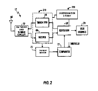
FIG. 2 is a block diagram illustrating an RF reader unit 12 in accordance with
one
embodiment of the present disclosure. As illustrated, the reader unit 12
includes: an antenna
60, a matching and tuning circuit 62, a resonance circuit 210 that includes a
transmitter 64
and a receiver 66, a controller 68, a current sensor 70, a comparator 72, a
compensation
circuit 220 and a user interface 74. While comparator 72 is drawn in FIG. 2 as
a separate
physical component, some or all of the functionality of comparator 72 can be
implemented by
controller 68. Namely, rather than being implemented by a hardware element,
the
6
CA 03159892 2022-5-27
WO 2021/110508
PCT/EP2020/083353
functionality of the comparator 72 can be implemented in software by
controller 68. In such
cases, the output of the current sensor 70 is provided directly to the
controller 68.
The controller 68 is operative for controlling the operation of the reader
unit 12 in
order to interrogate, track, and report on items-of-interest within the
coverage region 52 of
the reader unit 12. The controller 68 is implemented using a digital
processing device, such as
a general-purpose microprocessor, a digital signal processor, a reduced
instruction set
computer, a complex instruction set computer, or a field programmable gate
array. In
addition, one or more of the other functional blocks illustrated in FIG. 2 can
also be
implemented digitally within the same (or a different) digital processor as
the controller 68.
The transmitter 64 is used to generate interrogation signals (under the
control of the
controller 68) for transmission into the coverage region 52 via antenna 60
during an
interrogation operation. The transmitter 64 can also be used to generate an
acknowledgment
signal for delivery to a specific RF tag after identification information has
been received from
the tag, as described above. The receiver 66 is operative for, among other
things, receiving,
demodulating, and decoding identification signals received from RF tags
located within the
coverage region 52 and for delivering the resulting identification information
to the controller
68.
The matching and tuning circuit 62 is a device that improves the efficiency
with
which power available from a driver is delivered to the antenna 60. Impedances
at the
antenna 60 can he too high for low-voltage drivers to be able to develop
enough power
directly and, in such cases, a matching network is used to compensate for and
match the
impedances at the antenna 60. In addition to the impedance matching in the
case of inductive
coupling RF1D systems, the matching and tuning circuit 62 can also be used to
set the
resonance frequency of the antenna 60 correctly.
As the controller 68 collects tag identification information from the
corresponding
coverage region 52, it reports the data to an appropriate entity via user
interface 74.
Alternatively, the controller 68 can wait until all of the tag information has
been collected for
the coverage region 52 before it reports the data. The user interface 74 can
take many
different forms depending upon the type of reporting being done within the
system. For
example, the interface 74 can be coupled to a video display for displaying the
identification
data to an operator. Alternatively, the interface 74 could include a modem for
transferring the
data to a remote computer for storage. In some embodiments, the reader unit in
a large RFID
system interfaces via interface 74 to a central control processor that
assembles, manages, and
analyzes the identification information to generate a system wide report. The
central control
7
CA 03159892 2022-5-27
WO 2021/110508
PCT/EP2020/083353
processor can also use the information to perform other system functions such
as activating
electric door locks, sending messages to user displays (including a display on
the reader
itself), sounding alarms, and activating recording devices (e.g., a video
camera). Other forms
of user interface 74 can also be used.
In some embodiments, the controller 68 detects a change in a resonance
frequency of
the reader 12. Specifically, the controller 68 detects a change in the
resonance frequency of
the resonance circuit 210. In some implementations, the controller 68 detects
the change in
the resonance frequency based on an amount of current being driven to the
reader 12, and
specifically to the resonance circuit 210. In particular, a current sensor 70
is coupled to the
resonance circuit 210 and measures the amount of current driven to the
resonance circuit 210.
The current sensor 70 provides the measured current value to the comparator
72. The
comparator 72 accesses a preset threshold and determines whether the measured
current value
received from the current sensor 70 falls outside the threshold. In some
cases, the comparator
72 determines whether the measured current falls below a threshold value. In
some cases, the
comparator 72 determines whether the measured current exceeds a threshold
value. In some
cases, the comparator 72 determines whether the measured current falls outside
of a threshold
range. Namely, the threshold could be a specific value, such as a value that
is 10% higher or
10% lower than the normal current, or it could be a range, such as within 10%
of the normal
current.
The preset threshold of the comparator 72 represents an expected amount of
current
drawn by the resonance circuit 210 under normal operations. When the current
falls outside
of the preset threshold, the comparator 72 provides an indication to the
controller 68. The
indication may inform the controller 68 that a metal material is in close
proximity to the
reader 12. In response to determining that the current is above a preset
value, below a preset
value, or outside of a range of values, the controller 68 may detect that the
resonance
frequency of the inductive coupling reader has changed by an amount that falls
outside a
threshold. In such cases, the controller 68 activates the compensation circuit
220 to couple
one or more capacitors in parallel with the resonance circuit 210 to offset
the change in the
resonance frequency.
As an example, the preset threshold may be set to a value that is 10% higher
or 10%
lower than the value of the current drawn by the resonance circuit 210 (e.g.,
an antenna of the
resonance circuit 210) when no metal material is in close proximity to the
reader 12. The
preset threshold may be programmed into a look-up table or memory during
manufacture of
the reader 12 and/or may be dynamically updated based on different operating
conditions.
8
CA 03159892 2022-5-27
WO 2021/110508
PCT/EP2020/083353
The comparator 72 may periodically or continuously retrieve the preset
threshold from the
look-up table or memory to compare with the current being measured by the
current sensor
70.
In some embodiments, after the controller 68 activates the compensation
circuit 220,
the controller 68 may instruct the current sensor 70 to re-measure the current
drawn by the
resonance circuit 210. The re-measured current is compared by the comparator
72 to the
preset threshold to determine whether a change in the resonance frequency of
the resonance
circuit 210 still falls outside the threshold. As an example, after activating
the compensation
circuit 220, the current measured by the current sensor 70 may now be within
5% of the
normal operating current driven to the resonance circuit 210. The preset
threshold may be set
to a value that is 10% higher or lower than the normal operating current and,
in such cases,
the controller 68 may determine that the change in the resonance frequency of
the resonance
circuit 210 no longer falls outside the threshold (e.g., because the current
measured by the
current sensor 70 is not 10% more than or 10% less than the normal operating
current of the
resonance circuit 210).
In some embodiments, after the controller 68 activates the compensation
circuit 220,
the controller 68 may determine the current measured by the current sensor 70
may now be
12% greater than the normal operating current driven to the resonance circuit
210. Namely,
the change in the resonance frequency of the resonance circuit 210 may still
fall outside the
threshold even though the compensation circuit 220 is activated. In such
cases, the controller
68 may instruct the compensation circuit 220 to couple one or more additional
capacitors in
parallel with the resonance circuit 210 (e.g., to increase the total parallel
capacitance coupled
to the resonance circuit 210).
As an example, the compensation circuit 220 may include first and second
compensation circuits. The first compensation circuit may include a first
capacitor and the
second compensation circuit may include a second capacitor. The first
capacitor may be of
the same size and value as the second capacitor. In such cases, the controller
68 determines
that the change in the resonance frequency of the resonance circuit 210 falls
outside a first
threshold but is within a second threshold. For example, a first threshold may
be set to a
value of 10% greater than the normal operating current drawn by the resonance
circuit 210
and the second threshold may be set to a value that is 15% greater than the
normal operating
current drawn by the resonance circuit 210. The controller 68 may determine
that the current
being drawn by the resonance circuit 210 is 12% greater than the normal
operating current
drawn by the resonance circuit 210. In such cases, the controller 68
determines that the
9
CA 03159892 2022-5-27
WO 2021/110508
PCT/EP2020/083353
change in the resonance frequency of the resonance circuit 210 (resulting from
current being
drawn by the resonance circuit 210 by an amount that is 12% greater than the
normal
operating current) falls outside the first threshold but is within the second
threshold. In
response, the controller 68 activates the first compensation circuit. By
activating the first
compensation circuit, the controller 68 couples the first capacitor in
parallel to the resonance
circuit 210.
In some cases, after activating the first compensation circuit or at some
other time
before the first compensation circuit is activated, the controller 68 measures
the current
driven to the resonance circuit 210. The controller 68 determines that the
change in the
resonance frequency falls outside the first threshold and the second
threshold. For example,
the controller 68 may determine that the current being drawn by the resonance
circuit 210 is
17% greater than the normal operating current drawn by the resonance circuit
210. In such
cases, the controller 68 determines that the change in the resonance frequency
of the
resonance circuit 210 (resulting from current being drawn by the resonance
circuit 210 by an
amount that is 17% greater than the normal operating current) falls outside
the first threshold
(e.g., set to a value of 10% greater than the normal operating current) and
the second
threshold (e.g., set to a value of 15% greater than the normal operating
current). In response,
the controller 68 activates the second compensation circuit. By activating the
second
compensation circuit, the controller 68 couples the first and second
capacitors in parallel to
the resonance circuit 210.
In some implementations, the first capacitor may be smaller than the second
capacitor.
In such cases, activation of the second compensation circuit couples a larger
capacitor in
parallel with the resonance circuit 210 and decouples the smaller capacitor of
the first
compensation circuit from the resonance circuit 210. Namely, only one of the
first and
second compensation circuits is coupled to the resonance circuit 210 at a time
when different
size capacitors are implemented by the respective compensation circuits.
In some embodiments, the first or second compensation circuits are coupled in
parallel with the resonance circuit 210 by way of a switch, such as a
transistor. For example,
when the controller 68 activates (closes) a switch of the compensation circuit
220, one or
more capacitors of the compensation circuit 220 may be coupled in parallel to
the resonance
circuit 210. When the switch is de-activated (opened), the one or more
capacitors are
decoupled from the resonance circuit 210.
In some embodiments, the value of the capacitor or capacitance in the
compensation
circuit 220 is determined when the reader 12 is manufactured. In one example,
to do so, the
CA 03159892 2022-5-27
WO 2021/110508
PCT/EP2020/083353
reader 12 is mounted on a metal surface or material. A detuning effect on the
resonance
circuit 210 of the reader 12 is measured. As an example, the current sensor
may output a first
current value being drawn by the resonance circuit 210 when the reader 12 is
not mounted on
the metal surface or material. This first current value may represent the
expected current
drawn by the resonance circuit 210 under normal operating conditions. In some
cases, the
threshold may be computed as a function or factor of this expected current
(e.g., the threshold
may be set to a value of 10% greater than the first current value). In some
cases, after the
reader 12 is mounted on a metal surface or material, the current sensor may
output a second
current value being drawn by the resonance circuit 210. In such
implementations, the
threshold may be set to the value of the second current value or set to some
value that is
based on or is a function of the second current value but is higher or lower
than the second
current value. After the reader 12 is mounted on the metal surface, one or
more capacitors
may be coupled in parallel to the resonance circuit 210 until a capacitor
value is determined
that causes the current measured by the current sensor to be substantially
close to the first
current value. This capacitor value may be used to set the capacitor value of
the
compensation circuit 220. As such, when the reader 12 is operating in close
proximity to a
metal surface (e.g., as determined by the current measured by the current
sensor 70 exceeding
a threshold value), the controller 68 activates the compensation circuit 220
to couple the
capacitor value in parallel to the resonance circuit 210 to offset a change in
the resonance
frequency of the resonance circuit 210.
In some embodiments, the capacitor value(s) can be determined mathematically
(e.g.,
without actually mounting the reader 12 on a metal surface during
manufacture). In some
cases, the capacitor value(s) may be determined based on an expected metal
material on
which the reader 12 will be set during operation.
FIG. 3 is a block diagram illustrating a reader unit for use in an RFID system
in
accordance with various embodiments. As shown in FIG. 3, control circuitry 68
may be
coupled to a resonance circuit and a compensation circuit. Contorl circuitry
68 may include
and/or implement the functionality of controller 68. The control circuitry 68
measures
current drawn by the resonance circuit. In response to determining that the
current drawn by
the resonance circuit exceeds a threshold, the controller 68 activates a
switch 320. As a
result, a compensation capacitor 310 becomes coupled in parallel with the
resonance circuit.
Namely, a first terminal of the compensation capacitor 310 is coupled to
ground via a diode
330 and the switch 320. When the switch is de-activated, the compensation
capacitor 310 is
not coupled to ground and, as such, is decoupled from the resonance circuit.
When the
11
CA 03159892 2022-5-27
WO 2021/110508
PCT/EP2020/083353
switch 320 is closed, the first terminal of the compensation capacitor 310 is
coupled to
ground via the diode 330 and the switch 320. A second terminal of the
compensation
capacitor 310 is coupled to first terminals of one or more capacitors of the
resonance circuit.
Second terminals of the one or more capacitors of the resonance circuit are
coupled to
ground. In this way, the compensation capacitor 310 can be coupled in parallel
with the
capacitors of the resonance circuit when the switch 320 is activated or
closed.
FIG. 4 is a flow diagram depicting an example process 400 for operating an
inductive
coupling reader in accordance with various embodiments.
At operation 410, the inductive coupling reader detects a change in a
resonance
frequency of the inductive coupling reader.
At operation 420, the inductive coupling reader compares the change in the
resonance
frequency to a threshold.
At operation 430, the inductive coupling reader determines that the change in
the
resonance frequency falls outside the threshold.
At operation 440, the inductive coupling reader activates a compensation
circuit to
offset the change in the resonance frequency of the inductive coupling reader
in response to
determining that the change in the resonance frequency falls outside the
threshold.
FIG. 5 is a block diagram of an example machine 500 upon which any one or more
of
the techniques (e.g., methodologies) discussed herein may be performed and/or
that can be
included in the reader discussed above. In alternative embodiments, the
machine 500 may
operate as a standalone device or may be connected (e.g., networked) to other
machines. In a
networked deployment, the machine 500 may operate in the capacity of a server
machine, a
client machine, or both in server-client network environments. In an example,
the machine
500 may act as a peer machine in a peer-to-peer (P2P) (or other distributed)
network
environment. The machine 500 may be a personal computer (PC), a tablet PC, a
set-top box
(STB), a personal digital assistant (PDA), a mobile telephone, a web
appliance, an IoT
device, an automotive system, an aerospace system, or any machine capable of
executing
instructions (sequential or otherwise) that specify actions to be taken by
that machine.
Further, while only a single machine is illustrated, the term "machine" shall
also be taken to
include any collection of machines that individually or jointly execute a set
(or multiple sets)
of instructions to perform any one or more of the methodologies discussed
herein, such as via
cloud computing, software as a service (SaaS), or other computer cluster
configurations.
Examples, as described herein, may include, or may operate by, logic,
components,
devices, packages, or mechanisms. Circuitry is a collection (e.g., set) of
circuits implemented
12
CA 03159892 2022-5-27
WO 2021/110508
PCT/EP2020/083353
in tangible entities that include hardware (e.g., simple circuits, gates,
logic, etc.). Circuitry
membership may be flexible over time and underlying hardware variability.
Circuitries
include members that may, alone or in combination, perform specific tasks when
operating.
In an example, hardware of the circuitry may be immutably designed to carry
out a specific
operation (e.g., hardwired). In an example, the hardware of the circuitry may
include variably
connected physical components (e.g., execution units, transistors, simple
circuits, etc.)
including a computer-readable medium physically modified (e.g., magnetically,
electrically,
by moveable placement of invariant-massed particles, etc.) to encode
instructions of the
specific operation. In connecting the physical components, the underlying
electrical
properties of a hardware constituent are changed, for example, from an
insulator to a
conductor or vice versa. The instructions enable participating hardware (e.g.,
the execution
units or a loading mechanism) to create members of the circuitry in hardware
via the variable
connections to carry out portions of the specific tasks when in operation.
Accordingly, the
computer-readable medium is communicatively coupled to the other components of
the
circuitry when the device is operating. In an example, any of the physical
components may be
used in more than one member of more than one circuitry. For example, under
operation,
execution units may be used in a first circuit of a first circuitry at one
point in time and reused
by a second circuit in the first circuitry, or by a third circuit in a second
circuitry, at a
different time.
The machine (e.g., computer system) 500 may include a hardware processor 502
(e.g.,
a central processing unit (CPU), a graphics processing unit (GPU), a hardware
processor
core, or any combination thereof, such as a memory controller, etc.), a main
memory 504,
and a static memory 506, some or all of which may communicate with each other
via an
interlink (e.g., bus) 508. The machine 500 may further include a display
device 510, an
alphanumeric input device 512 (e.g., a keyboard), and a user interface (UI)
navigation device
514 (e.g., a mouse). In an example, the display device 510, alphanumeric input
device 512,
and LTI navigation device 514 may be a touchscreen display. The machine 500
may
additionally include a storage device 522 (e.g., drive unit); a signal
generation device 518
(e.g., a speaker); a network interface device 520; one or more sensors 516,
such as a Global
Positioning System (GPS) sensor, wing sensors, mechanical device sensors,
temperature
sensors, ICP sensors, bridge sensors, audio sensors, industrial sensors, a
compass, an
accelerometer, or other sensors; and one or more system-in-package data
acquisition devices
590. The system-in-package data acquisition device(s) 590 may implement some
or all of the
13
CA 03159892 2022-5-27
WO 2021/110508
PCT/EP2020/083353
functionality of the offset calibration system 100. The machine 500 may
include an output
controller 528, such as a serial (e.g., universal serial bus (USD)), parallel,
or other wired or
wireless (e.g., infrared (R), near field communication (NFC), etc.) connection
to
communicate with or control one or more peripheral devices (e.g., a printer,
card reader, etc.).
The storage device 522 may include a machine-readable medium on which is
stored
one or more sets of data structures or instructions 524 (e.g., software)
embodying or utilized
by any one or more of the techniques or functions described herein. The
instructions 524 may
also reside, completely or at least partially, within the main memory 504,
within the static
memory 506, or within the hardware processor 502 during execution thereof by
the machine
500. In an example, one or any combination of the hardware processor 502, the
main memory
504, the static memory 506, or the storage device 521 may constitute the
machine-readable
medium.
While the machine-readable medium is illustrated as a single medium, the term
"machine-readable medium" may include a single medium or multiple media (e.g.,
a
centralized or distributed database, or associated caches and servers)
configured to store the
one or more instructions 524.
The term "machine-readable medium" may include any transitory or non-
transitory
medium that is capable of storing, encoding, or carrying transitory or non-
transitory
instructions for execution by the machine 500 and that cause the machine 500
to perform any
one or more of the techniques of the present disclosure, or that is capable of
storing,
encoding, or carrying data structures used by or associated with such
instructions. Non-
limiting machine-readable medium examples may include solid-state memories,
and optical
and magnetic media. In an example, a massed machine-readable medium comprises
a
machine-readable medium with a plurality of particles having invariant (e.g.,
rest) mass.
Accordingly, massed machine-readable media are not transitory propagating
signals. Specific
examples of massed machine-readable media may include non-volatile memory,
such as
semiconductor memory devices (e.g., Electrically Programmable Read-Only Memory
(EPROM), Electrically Erasable Programmable Read-Only Memory (EEPROM)) and
flash
memory devices; magnetic disks, such as internal hard disks and removable
disks; magneto-
optical disks; and CD-ROM and DVD-ROM disks.
The instructions 524 (e.g., software, programs, an operating system (OS),
etc.) or
other data that are stored on the storage device 521 can be accessed by the
main memory 504
for use by the hardware processor 502. The main memory 504 (e.g., DRAM) is
typically fast,
but volatile, and thus a different type of storage from the storage device 521
(e.g., an SSD),
14
CA 03159892 2022-5-27
WO 2021/110508
PCT/EP2020/083353
which is suitable for long-term storage, including while in an "off'
condition. The
instructions 524 or data in use by a user or the machine 500 are typically
loaded in the main
memory 504 for use by the hardware processor 502. When the main memory 504 is
full,
virtual space from the storage device 521 can be allocated to supplement the
main memory
504; however, because the storage device 521 is typically slower than the main
memory 504,
and write speeds are typically at least twice as slow as read speeds, use of
virtual memory can
greatly reduce user experience due to storage device latency (in contrast to
the main memory
504, e.g., DRAM). Further, use of the storage device 521 for virtual memory
can greatly
reduce the usable lifespan of the storage device 521.
The instructions 524 may further be transmitted or received over a
communications
network 526 using a transmission medium via the network interface device 520
utilizing any
one of a number of transfer protocols (e.g., frame relay, internet protocol
(IP), transmission
control protocol (TCP), user datagram protocol (UDP), hypertext transfer
protocol (HTTP),
etc.). Example communication networks may include a local area network (LAN),
a wide
area network (WAN), a packet data network (e.g., the Internet), mobile
telephone networks
(e.g., cellular networks), Plain Old Telephone Service (POTS) networks, and
wireless data
networks (e.g., Institute of Electrical and Electronics Engineers (IEEE)
802.11 family of
standards known as Wi-Fi , IEEE 802.16 family of standards known as WiMax ,
IEEE
802.15.4 family of standards, peer-to-peer (P2P) networks), among others. In
an example, the
network interface device 520 may include one or more physical jacks (e.g.,
Ethernet, coaxial,
or phone jacks) or one or more antennas to connect to the communications
network 526. In
an example, the network interface device 520 may include a plurality of
antennas to
wirelessly communicate using at least one of single-input multiple-output
(S1M0), multiple-
input multiple-output (MIMO), or multiple-input single-output (MISO)
techniques. The term
"transmission medium" shall be taken to include any tangible or intangible
medium that is
capable of storing, encoding, or carrying instructions for execution by the
machine 500, and
includes digital or analog communications signals or other tangible or
intangible media to
facilitate communication of such software.
Each of the non-limiting aspects or examples described herein may stand on its
own,
or may be combined in various permutations or combinations with one or more of
the other
examples.
The above detailed description includes references to the accompanying
drawings,
which form a part of the detailed description. The drawings show, by way of
illustration,
specific embodiments in which the inventive subject matter may be practiced.
These
CA 03159892 2022-5-27
WO 2021/110508
PCT/EP2020/083353
embodiments are also referred to herein as "examples.." Such examples may
include elements
in addition to those shown or described. However, the present inventors also
contemplate
examples in which only those elements shown or described are provided.
Moreover, the
present inventors also contemplate examples using any combination or
permutation of those
elements shown or described (or one or more aspects thereof), either with
respect to a
particular example (or one or more aspects thereof), or with respect to other
examples (or one
or more aspects thereof) shown or described herein.
In the event of inconsistent usages between this document and any documents so
incorporated by reference, the usage in this document controls.
In this document, the terms "a" or "an" are used, as is common in patent
documents,
to include one or more than one, independent of any other instances or usages
of "at least
one" or "one or more." In this document, the term "or" is used to refer to a
nonexclusive or,
such that "A or B" includes "A but not B," "B but not A," and "A and B,"
unless otherwise
indicated. In this document, the terms "including" and "in which" are used as
the plain-
English equivalents of the respective terms "comprising" and "wherein." Also,
in the
following claims, the terms "including" and "comprising" are open-ended; that
is, a system,
device, article, composition, formulation, or process that includes elements
in addition to
those listed after such a term in a claim are still deemed to fall within the
scope of that claim.
Moreover, in the following claims, the terms "first," "second," "third," etc.,
are used merely
as labels, and are not intended to impose numerical requirements on their
objects.
Method examples described herein may be machine- or computer-implemented at
least in part. Some examples may include a computer-readable medium or machine-
readable
medium encoded with transitory or non-transitory instructions operable to
configure an
electronic device to perform methods as described in the above examples. An
implementation
of such methods may include code, such as microcode, assembly-language code, a
higher-
level-language code, or the like. Such code may include transitory or non-
transitory
computer-readable instructions for performing various methods. The code may
form portions
of computer program products. Further, in an example, the code may be tangibly
stored on
one or more volatile, non-transitory, or non-volatile tangible computer-
readable media, such
as during execution or at other times. Examples of these tangible computer-
readable media
may include, but are not limited to, hard disks, removable magnetic disks,
removable optical
disks (e.g., compact discs and digital video discs), magnetic cassettes,
memory cards or
sticks, random access memories (RAMs), read-only memories (ROMs), and the
like.
16
CA 03159892 2022-5-27
WO 2021/110508
PCT/EP2020/083353
The above description is intended to be illustrative, and not restrictive. For
example,
the above-described examples (or one or more aspects thereof) may be used in
combination
with each other. Other embodiments may be used, such as by one of ordinary
skill in the art
upon reviewing the above description. The Abstract is provided to comply with
37 C.F.R.
1.72(b), to allow the reader to quickly ascertain the nature of the technical
disclosure. It is
submitted with the understanding that it will not be used to interpret or
limit the scope or
meaning of the claims. Also, in the above detailed description, various
features may be
grouped together to streamline the disclosure. This should not be interpreted
as intending that
an unclaimed disclosed feature is essential to any claim. Rather, inventive
subject matter may
lie in less than all features of a particular disclosed embodiment. Thus, the
following claims
are hereby incorporated into the detailed description as examples or
embodiments, with each
claim standing on its own as a separate embodiment, and it is contemplated
that such
embodiments may be combined with each other in various combinations or
permutations.
The scope of the inventive subject matter should be determined with reference
to the
appended claims, along with the full scope of equivalents to which such claims
are entitled.
17
CA 03159892 2022-5-27