Note : Les descriptions sont présentées dans la langue officielle dans laquelle elles ont été soumises.
CA 03161140 2022-05-11
WO 2021/094485
PCT/EP2020/081963
1
Nanowires network
FIELD OF THE INVENTION
The present invention relates to the synthesis of a network of nanowires. More
specifically, the present invention relates to a process for preparing said
network of
nanowires.
BACKGROUND
Networks comprised of nanowires present advantages over materials made of
larger
building blocks. In general, nanowires are mechanically flexible due to their
nanoscale
dimensions and have a reduced amount of defects in comparison with bulk
materials.
They also display various optoelectronic properties resulting from their small
size and
one-dimensional morphology. Consequently, some of the properties of the
nanowires
networks depend on the characteristics of the nanowires. Thus a high degree of
control
over the nanowires' crystalline quality, morphology and size distribution is
needed.
Heurlin, M. et al. (Heurlin, M. et al. Nature volume 492, pages 90-94,2012)
discloses an
aerosol-based nanowire growth method (aerotaxy method) wherein catalytic size-
selected Au aerosol particles induce nucleation and growth of GaAs nanowires
at a
growth rate of about 1 micrometer per second. The effectivity of aerotaxy
method has
only been demonstrated for the synthesis of GaAs (GaAsNWs), P-, Zn- and Sn-
doped
GaAsNWs nanowires and InP nanoparticles (Magnusson, M. H. et al. Frontiers of
Physics, 9(3), 398-418,2014). W02013176619 (Al) describes a gas phase nanowire
synthesis method that claims to be able to grow individual silicon nanowires
followed by
a subsequent step of spraying said nanowires through a spray nozzle followed
by their
deposition onto a substrate to form a network of nanowires. According to
W02013176619 (Al) the spraying and deposition step may be performed right
after the
synthesis of nanowires or after the storage of said nanowires in a reservoir.
However,
two-step methods for synthesis of nanowire networks lead to nanowires
shortening and
therefore to degraded materials. Moreover, the nanowires forming the network
are not
permanently entangled or associated and need to be deposited on a supporting
substrate to generate self-standing materials.
CA 03161140 2022-05-11
WO 2021/094485
PCT/EP2020/081963
2
In summary, there is a need to develop one-step methods for synthesis of
networks of
nanowires with good mechanical properties that overcome prior art limitations.
BRIEF DESCRIPTION OF THE INVENTION
The inventors of the present invention have found a one-step method for
producing self-
standing networks of nanowires with good mechanical properties, such as good
flexibility
in bending, and wherein the nanowires have high aspect ratios. The discovery
of self-
standing networks of nanowires that are also flexible represents a
breakthrough since
they allow post-production manipulation of the nanowire network as an
engineering
material, rather than as a powder or filler which typically undergo
degradation and/or
nanowire shortening during dispersion upon processing. In addition, the
inventors have
observed that the method of the present invention allows the production of
networks of
nanowires in large amounts and at high rates. This approach is of great
importance for
a large variety of applications of networks of nanowires in various
technological fields,
since it solves the current limitations of the prior art.
The method of the present invention is based on aerosol technology and has the
potential of being scaled up to produce large amounts of product, while
maintaining a
high level of control over the process.
Thus, in a first aspect, the invention is directed to a method for preparing a
network of
nanowires comprising the steps of:
i. providing a first gas flow to a reaction vessel;
wherein said first gas flow comprises at least one precursor compound
comprising at least one element selected from Si, Ge, Al, B, Cu, Zn, Cd, Al,
Ga, In, As, Sb, Nb, Ni, Ti, Se, Ta, Pt, Mo, W, C, N, 0, Co, Mn, Li and Te;
and
ii. providing a second gas flow to the reaction vessel, said second gas
flow
comprising metallic catalyst particles; so as the first and second gas flows
are mixed in the reaction vessel to form a gas flow mixture;
wherein the at least one precursor compound is in the gas flow mixture in a
mole
fraction (xi) of at least 0.005;
wherein the temperature inside the reaction vessel ranges from 200 to 800 C
or
is at least 801 C; and
CA 03161140 2022-05-11
WO 2021/094485
PCT/EP2020/081963
3
wherein the at least one precursor compound decomposes under the
temperature inside the reaction vessel and grows on the metallic catalyst
particles by vapor liquid-solid (VLS) and/or chemical vapor deposition (CVD)
to
form a network of nanowires.
In a second aspect, the invention is directed to a network of nanowires
obtainable by the
method as defined above; wherein the aspect ratio (length/diameter) of the
nanowires
of the network of nanowires is at least 130.
In a third aspect, the present invention is directed to a nonwoven material
comprising
the network of nanowires of the present invention.
Another aspect of the invention is directed to an electrode comprising the
network of
nanowires of the present invention in any of its particular embodiments or the
nonwoven material of the present invention and optionally an electrical
connection or a
current collector, preferably comprising a conductive wire or a current
collector; wherein
the electrical connection or the current collector and the network of
nanowires are
electrically connected.
In a further aspect, the present invention is directed to the use of the
network of
nanowires of the present invention, in electronic devices, micromechanical
systems,
optoelectronic devices, wearable devices, insulators, sensors, electrodes,
catalysis,
structural elements, batteries, flexible devices, radiation absorbing material
and
transparent devices.
In a further aspect, the present invention is directed to the use of the
nonwoven materials
of the present invention, in electronic devices, micromechanical systems,
optoelectronic devices, wearable devices, insulators, sensors, electrodes,
catalysis,
structural elements, batteries, flexible devices, radiation absorbing material
and
transparent devices.
In a further aspect, the present invention is directed to a pharmaceutical
composition
comprising the network of nanowires of the invention or the nonwoven material
of the
invention.
CA 03161140 2022-05-11
WO 2021/094485
PCT/EP2020/081963
4
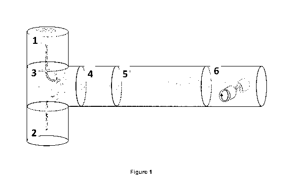
FIGURES
Figure 1 shows a sketch of the continuous synthesis system comprising (1) a
silicon
precursor flow entry, (2) an aerosol of catalyst nanoparticles flow entry, (3)
a mixing area of
the silicon precursor and the catalyst flow; (4) a silicon nanowire nucleation
area; (5) area
of elongation/growth and entanglement of silicon nanowires; and (6) area of
spinning,
drawing and/or collection of nonwoven materials (such as fibers) comprising
silicon
nanowires.
Figure 2 shows a transmission electron microscopy micrograph showing a silicon
nanowire.
Figure 3 shows scanning electron microscopy micrographs of the network of
silicon
nanowires obtained in the present invention.
Figure 4 shows a self-standing network of silicon nanowires obtained in the
present
invention.
Figure 5 shows a piece of the network of silicon nanowires obtained in the
present invention
under bending deformation.
Figure 6 shows mechanical tests results of nanowire networks.
DETAILED DESCRIPTION OF THE INVENTION
Unless defined otherwise, all technical and scientific terms used herein have
the same
meaning as commonly understood to one of ordinary skill in the art to which
this
disclosure belongs. As used herein, the singular forms "a" "an" and "the"
include plural
reference unless the context clearly dictates otherwise.
The present invention is directed to a method for preparing a network of
nanowires, to
the network of nanowires obtainable by said method, to a nonwoven material
comprising the network of nanowires, to the uses of the network of nanowires
of the
invention and the nonwoven material, and to a pharmaceutical composition
comprising
the network of nanowires of the invention or the nonwoven material of the
invention.
CA 03161140 2022-05-11
WO 2021/094485
PCT/EP2020/081963
The nanowires of the network of nanowires of the present invention are high
aspect
ratio structures that may be made of a solid material or may be hollow (having
a tube
shape). In an embodiment, the nanowires are continuous structures (not
porous). In
another embodiment, the nanowires form a net by joining among each other
during
5 .. their synthesis.
Method
In a first aspect, the invention is directed to a method for preparing a
network of
nanowires comprising the steps of:
i. providing a first gas flow to a reaction vessel;
wherein said first gas flow comprises at least one precursor compound
comprising at least one element selected from Si, Ge, Al, B, Cu, Zn, Cd, Al,
Ga, In, As, Sb, Nb, Ni, Ti, Se, Ta, Pt, Mo, W, C, N, 0, Co, Mn, Li, and Te;
and
ii. providing a second gas flow to the reaction vessel, said second gas
flow
comprising metallic catalyst particles; so as the first and second gas flows
are mixed in the reaction vessel to form a gas flow mixture;
wherein the at least one precursor compound is in the gas flow mixture in a
mole
fraction (xi) of at least 0.005;
wherein the temperature inside the reaction vessel ranges from 200 to 800 C
or
is at least 801 C; and
wherein the at least one precursor compound decomposes under the
temperature inside the reaction vessel and grows on the metallic catalyst
particles by vapor liquid-solid (VLS) and/or chemical vapor deposition (CVD)
to
form a network of nanowires.
The method for preparing a network of nanowires may comprise a further step of
transforming the network of nanowires into fibers, yarns or fabrics. The step
of
transforming the network of nanowires into fibers, yarns or fabrics is
optionally
performed at the same time than step (ii) of the method of the invention.
In a particular embodiment, the method for preparing a network of nanowires
comprises
a further step of collecting the network of nanowires; particularly by
spinning and
winding the network of nanowires (as a yarn or a fabric) on a bobbin.
CA 03161140 2022-05-11
WO 2021/094485
PCT/EP2020/081963
6
In an embodiment, the method of the present invention is a continuous
aggregated
method.
Step (I)
The method for preparing a network of nanowires of the present invention
comprises a
step (i) of providing a first gas flow to a reaction vessel; wherein said
first gas flow
comprises at least one precursor compound comprising at least one element
selected
from Si, Ge, Al, B, Cu, Zn, Cd, Al, Ga, In, As, Sb, Nb, Ni, Ti, Se, Ta, Pt,
Cu, Mo, W, C,
N, 0, Co, Mn, Li and Te.
In a particular embodiment, the first gas flow further comprises H2. In a
particular
embodiment, the first gas flow further comprises an inert gas, particularly N2
Precursor
The step (i) of the method of the present invention provides a first gas flow
to a reaction
vessel wherein said first gas flow comprises at least one precursor compound.
In a
particular embodiment, the at least one precursor compound is a compound that
participates in a reaction (i.e. chemical reaction) that produces the nanowire
network
of the present invention, for example, Sil-lais a precursor compound that when
used in
the method of the present invention may lead to a Si nanowire network.
In a particular embodiment, the at least one precursor compound of the method
of the
present invention comprises at least one element selected from Si, Ge, Al, B,
Cu, Zn,
Cd, Al, Ga, In, As, Sb, Nb, Ni, Ti, Se, Ta, Pt, Cu, Mo, W and Te; particularly
Si, Ge, In,
Ga, Se and Te; more particularly Si and Ge; even more particularly Si.
In a particular embodiment, the at least one precursor compound is one
precursor
compound.
The at least one precursor compound may be in solid or liquid form (i.e.
aerosolized in
the first gas flow of the method of the present invention) or in gas form. In
a particular
embodiment, the at least one precursor compound is in gas form.
CA 03161140 2022-05-11
WO 2021/094485
PCT/EP2020/081963
7
In a particular embodiment, the at least one precursor compound of the method
of the
present invention is a metallic hydride or an organometallic compound.
Precursors of
the present invention include but are not limited compounds such as (3-
Aminopropyl)triethoxysilane, N-sec-
Butyl(trimethylsilyl)amine,
chloropentamethyldisilane, tetramethylsilane, silicon
tetrabromide, silicon
tetrachloride, tris(tert-butoxy)silanol, SiH4, tetramethylgermanium,
triethylgermanium
hydride, triphenylgermanium hydride, triphenylgermanium
hydride,
tetramethylgermanium, tributylgermanium hydride, triethylgermanium hydride,
triphenylgermanium hydride, trimethylindium (TMin), trimethylindium (TEIN),
trimethylgallium (TMG), triethylgallium (TEG), dimethyl selenide, tellurium
tetrachloride, trimethylaluminium (TMAI), triethylaluminium (TEA!), NH3, AsH3
and PH3;
particularly silane derivates such as (3-Aminopropyl)triethoxysilane, N-sec-
Butyl(trimethylsilyl)amine, chloropentamethyldisilane, tetramethylsilane,
silicon
tetrabromide, silicon tetrachloride, tris(tert-butoxy)silanol, SiH4,
tetramethylgermanium,
triethylgermanium hydride, triphenylgermanium hydride, triphenylgermanium
hydride,
tetramethylgermanium, tributylgermanium hydride, triethylgermanium hydride,
triphenylgermanium hydride, trimethylindium (TMin), trimethylindium (TEIN),
trimethylgallium (TMG), triethylgallium (TEG), dimethyl selenide and tellurium
tetrachloride; more particularly silane derivates such as (3-
Aminopropyl)triethoxysilane, N-
sec-Butyl(trimethylsilyl)amine,
chloropentamethyldisilane, tetramethylsilane, silicon
tetrabromide, silicon
tetrachloride, tris(tert-butoxy)silanol, SiH4, tetramethylgermanium,
triethylgermanium
hydride, triphenylgermanium hydride, triphenylgermanium
hydride,
tetramethylgermanium, tributylgermanium hydride, triethylgermanium hydride and
triphenylgermanium hydride; even more particularly Si1-14
In a particular embodiment, the at least one precursor compound is a metallic
hydride,
particularly Si1-14
In a particular embodiment, the at least one precursor compound is an
organometallic
compound.
In a particular embodiment, the first gas flow comprises more than one
precursor
compound. In particular, the first gas flow comprises a first precursor
compound and
CA 03161140 2022-05-11
WO 2021/094485
PCT/EP2020/081963
8
additional precursor compounds. In a particular embodiment, the additional
precursor
compounds may be used as dopants of the nanowire network (in less amount that
the
main precursor compound). Suitable dopants depend on the nanowire material
being
doped.
In a particular embodiment, the at least one precursor compound of the present
invention is provided to the reaction vessel of the present invention at a
rate of at least
0.01 mol/h; preferably at a rate of at least 0.05 mol/h; more preferably of at
least 0.10
mol/h; even much more preferably of about 0.03 mol/h.
Step (ii)
The method for preparing a network of nanowires of the present invention
comprises a
step (ii) of providing a second gas flow to the reaction vessel, said second
glass flow
comprising metallic catalyst particles; so as the first and second gas flows
are mixed
in the reaction vessel to form a gas flow mixture.
In a particular embodiment, the second gas flow of the method of the present
invention
further comprises an inert gas, preferably N2.
In a more particular embodiment, the second gas flow of the method of the
present
invention further comprises H2.
In a particular embodiment only one type of gas is used in the invention. In
particular,
the terms "first" and "second" are referred to the number of flows used.
Catalyst
The method for preparing a network of nanowires of the present invention
comprises a
step (ii) of providing a second gas flow comprising metallic catalyst
particles.
In a particular embodiment, the metallic catalyst particles of the method of
the present
invention comprise one or more element selected from Au, Ag, Cu, Fe, Ni, Ga,
Co, Pt,
In and Al; particularly comprise one or more element selected from Au, Ni, Ag
and Cu;
more particularly comprise one or more element selected from Au and Ag; even
more
CA 03161140 2022-05-11
WO 2021/094485
PCT/EP2020/081963
9
particularly comprise Au. The metallic catalytic particles may consist of a
single
element, or a combination (e.g. alloy) of two or more elements. The metallic
catalyst
particles may be in the second gas flow as solid particles or as liquid
particles;
preferably as solid particles.
In another particular embodiment, the metallic catalyst particles of the
method of the
present invention further comprise one or more additional elements selected
from
group 16 elements to control and/or enhance the growth of nanowires. This
additional
elements are particularly selected from oxygen, sulfur, selenium, tellurium,
and
polonium; more particularly selected from S, Se, Te and 0.
In a particular embodiment, the metallic catalyst particles consist of one
element
selected from Au, Ag, Cu, Fe, Ni, Ga, Co, Pt, In and Al; particularly consist
of one
element selected from Au, Ag and Cu; more particularly consist of one element
selected from Au and Ag; even more particularly consist of Au.
In a particular embodiment, the metallic catalyst particles have an averaged
diameter
of between 0.1 and 100 nm; preferably of between 1 and 30 nm. The average
diameters
of the metallic catalyst particles of the present invention may be calculated
from an
average of the values obtained by measuring the diameters of more than 100
metallic
catalyst particles using electronic microscopy micrographs or from the size
distribution
obtained from different aerosol measuring technics such as from a Differential
Mobility
Particle Sizer (DMA).
Furthermore, the metallic catalyst particles may be provided without
electrical charge
or the metallic catalytic particles may be given a charge.
The metallic catalyst particles may be provided to the reaction vessel in the
form of an
aerosol generated by an upstream aerosol generator. Alternatively, the
metallic
catalyst particles may be formed in-situ by providing a precursor compound;
preferably
a gaseous precursor compound. In a preferred embodiment, the metallic catalyst
particles are provided in the form of an aerosol.
In a particular embodiment, the metallic catalyst particles enter the reaction
vessel at
a rate of at least 1 x 10⁻⁵ g/h; preferably of at least 1 x 10⁻⁴ g/h; more
preferably of at
CA 03161140 2022-05-11
WO 2021/094485
PCT/EP2020/081963
least 2 x 10⁻⁴ g/h; even more preferably of at least 2.7 x 10⁻⁴ g/h.
Gas flow mixture
In a particular embodiment the gas flow mixture of the method of the present
invention
5 is generated when the first and the second gas flow are in contact in the
reaction
vessel. Means for mixture may be used to mix the flows to form a gas flow
mixture.
Pressure and flow rates might be adjusted if necessary to ensure a proper
mixture of
the first and second flow to form a gas flow mixture.
10 In a particular embodiment, the gas flow mixture circulates in the
reaction vessel at a
rate of at least 60 l/h; preferably at least 120 l/h.
In another particular embodiment, the gas flow mixture has a residence time in
the
reaction vessel of less than 100 seconds; particularly of between 0.1 and 80
seconds;
more particularly of between 1 and 60 seconds; even more particularly of
between 2
and 30 seconds; preferably of between 4 and 16 seconds.
In addition to the gas flow mixture, one or more sheath flows may be
introduced in the
reaction vessel of the present invention. Sheath flows include, but are not
limited to,
nitrogen, hydrogen and noble gases such as helium and argon.
In the method of the present invention the at least one precursor compound is
in the
gas flow mixture in a mole fraction (xi) of at least 0.005.
In a particular embodiment, the at least one precursor compound is in the gas
flow
mixture in a mole fraction of at least 0.006; particularly of at least 0.01;
more particularly of
at least 0.015; even more particularly of between 0.01 and 0.5; preferably of
about 0.02. In
the context of the present invention, the mole fraction is expressed as the
amount of a
constituent (in moles), divided by the total amount of all constituents (also
expressed in
moles).
In a particular embodiment, the at least one precursor compound of the present
invention is in the gas flow mixture in a concentration of at least 0.1'10-4
mo1/1;
particularly in a concentration of at least 1'10-4 mo1/1; more particularly in
a
concentration of at least 1.5*10-4 mo1/1; even more particularly of at least
2*10-4 mo1/1.
CA 03161140 2022-05-11
WO 2021/094485
PCT/EP2020/081963
11
In a particular embodiment, the gas flow mixture comprises H2
In an embodiment, the gas flow mixture of the invention comprises:
- at least one precursor compound;
- at least a sheath gas such as nitrogen, hydrogen and/or noble gases; and
- metallic catalyst particles.
In an embodiment, the gas flow mixture of the invention consist of:
- at least one precursor compound;
- at least a sheath gas such as nitrogen, hydrogen and/or noble gases; and
- metallic catalyst particles.
In a preferred embodiment, the gas flow mixture of the invention consist of:
- a precursor compound such as SiH4;
- a sheath gas or gas mixture such as nitrogen, hydrogen, noble gases of
combinations thereof; and
metallic catalyst particles such as gold particles.
Reaction vessel
In a particular embodiment, the reaction vessel used in the process of the
present
invention is a gas reaction vessel; preferably a cylindrical reaction vessel;
more
preferably a ceramic or metallic cylindrical reaction vessel; even more
preferably a
stainless steel cylindrical reaction vessel such as a tube.
According to the method of the present invention, the first and second gas
flows mix
inside the reaction vessel.
In a particular embodiment, the temperature inside the reaction vessel is
homogeneous; in particular is homogeneous within 50 degrees along the reactor
tube,
more particularly is homogeneous over 80 cm from the hot zone; particularly
between
30-50 cm of the hot zone.
In the method of the present invention, the temperature inside the reaction
vessel is at
least 200 C; preferably at least 400 C; more preferably at least 500 C.
CA 03161140 2022-05-11
WO 2021/094485
PCT/EP2020/081963
12
In a particular embodiment, the temperature inside the reaction vessel ranges
from 200
to 800 C or is at least 801 C; this temperatures allow the precursor compound
to
decompose; preferably the temperature ranges from 200 to 800 C or from 801 to
3000 C; more preferably the temperature ranges from 300 to 800 C or from 801
to
2000 C.
In a particular embodiment, the temperature inside the reaction vessel ranges
from 200
to 800 C; preferably the temperature ranges from 300 to 700 C; more preferably
from
400 to 650 C; even more preferably is about 600 C.
In a particular embodiment, the pressure inside the reaction vessel is between
500
mbar to 20000 mbar (50000 Pa to 2000000 Pa); preferably between 900 mbar to
3000
mbar (90000 Pa to 300000 Pa).
In a particular embodiment, the temperature inside the reaction vessel is
reached by
any suitable means of heating known in the art; preferably by plasma, arc
discharge,
resistive heating, hot wire heating, torch heating, or flame heating means;
more
preferably by resistive heating, hot wire heating, torch heating, or flame
heating means.
Nanowire network growth
In the method of the present invention, the at least one precursor compound
decomposes under the temperature conditions inside the reaction vessel and
grows
on the metallic catalyst particles by vapor liquid-solid (VLS) and/or chemical
vapor
deposition (CVD) to form a network of nanowires. In a particular embodiment
the
nanowires grow while being in the gas flow mixture (i.e. they are
aerosolized). In a
particular embodiment, the at least one precursor compound decomposes under
the
temperature conditions inside the reaction vessel and grows on the metallic
catalyst
particles by floating catalyst chemical vapor deposition (CVD) to form a
network of
nanowires.
If necessary, one or more sheath flows may be introduced in the reaction
vessel. In
particular, said one or more sheath flows might be introduced between the gas
flow
mixture and the walls of the reaction vessel.
CA 03161140 2022-05-11
WO 2021/094485
PCT/EP2020/081963
13
By choosing appropriate precursor compounds, gas flows, temperatures,
pressures,
and metallic catalyst particles, the nanowires can be grown in the axial or
radial
direction, or in a combination of the two growth modes; preferably growth
occurs in
axial direction; more preferably growth occurs in the 110 direction;
particularly for Si
nanowires.
Nanowire growth may be initiated by catalytic decomposition of the at least
one
precursor compound on the surface of the metallic catalyst particles and
nucleation of
the nanowire on the surface of the metallic catalytic particles. After
nucleation, the
nanowire may grow directionally and form an elongated object, i.e. a nanowire.
Growth
may occur via vapor liquid-solid (VLS) and/or chemical vapor deposition (CVD).
At the
same time, the nanowires reach a critical concentration and aggregate to form
a
network of nanowires in the reaction vessel. Thus, the method of the present
invention
is a continuous aggregated method. Preferably, the gas mixture flows through
the
reactor carrying metallic catalytic particles and the nanowire network flows
through the
reaction vessel length. In an embodiment, the network of nanowires comprises
hollow
nanowires such as nanotubes. In an embodiment the network of nanowires
comprises
hollow and not hollow nanowires such as solid nanowires. In another
embodiment, the
network of nanowires consist of hollow nanowires such as nanotubes.
In the context of the present invention, the expression chemical vapor
deposition (CVD)
is understood as a process in which one or more volatile precursor compounds
react
and/or decompose on a catalyst surface to produce one-dimensional structures,
such
as nanowires. Said catalyst particle may be suspended in the gas phase,
commonly
referred to as floating catalyst. Said particles may be in molten or solid
state and may
include additional elements to control and/or enhance growth of nanowires as
described herein above. This additional elements include group 16 elements,
such as
S, Se, Te, or oxygen. Said precursors may also partially decompose on the
surface of
the reactor.
In a particular embodiment, the method for preparing a network of nanowires of
the
present invention is performed under an aerogelation parameter of at least 1 *
10-7;
particularly under an aerogelation parameter of at least 1 * 10-6; more
particularly under
an aerogelation parameter of at least 2 * 10-6.
CA 03161140 2022-05-11
WO 2021/094485
PCT/EP2020/081963
14
In the context of the present invention, the expression "aerogelation
parameter" is
understood as the product of the average aspect ratio of the nanowires
(length/diameter)
and the volumetric concentration (vc (volume of nanowires/volume of the
reactor)).
In the context of the present invention, the expression "vapor¨liquid¨solid"
(VLS) is a
mechanism for the growth of one-dimensional structures, such as nanowires,
from
chemical vapor deposition by direct adsorption of a gas (i.e. the at least one
precursor
compound on gas phase) on to a liquid catalyst particle, which can rapidly
adsorb a
vapor to supersaturation levels, and from which crystal growth can occur from
nucleated seeds at the gas-liquid-solid interface.
In a particular embodiment, a nanowire network of the present invention is
formed while
being in the gas flow mixture (in the reaction vessel), particularly, a
network of
nanowires wherein the nanowires are aggregated (i.e. the nanowires are joined,
entangled, connected or fused among them) is obtained at the exit of the
reaction
vessel of the present invention.
In a particular embodiment, the network of nanowires of the present invention
is
generated as a continuous process. Alternatively, the network of nanowires may
be
discretely generated. In a preferred embodiment, the network of nanowires of
the
present invention is continuously generated.
In a particular embodiment, the method of the present invention further
comprises a
step of collecting the network of nanowires on a substrate; preferably wherein
the
substrate is a filter; more preferably a vacuum filter. In a more particular
embodiment,
the method of the present invention further comprises a step of densification
of the
network of nanowires; preferably by using a solvent or a mixture of solvents;
more
preferably an organic solvent or a mixture of organic solvents; even more
preferably a
solvent or a mixture of solvents comprising an alcohol group; even much more
preferably using isopropanol.
In a particular embodiment, the network of nanowires of the present invention
is
generated at a rate of at least 0.01 g/h; preferably at a rate of at least
0.02 g/h; more
preferably at a rate of at least 0.05 g/h; even more preferably at a rate of
about 0.1 g/h.
CA 03161140 2022-05-11
WO 2021/094485
PCT/EP2020/081963
In another particular embodiment, the network of nanowires of the present
invention is
generated at a rate of between 0.01 g/h and 10 g/h; preferably at a rate of
between
0.02 g/h and 5 g/h; more preferably at a rate of between 0.05 g/h and 1 g/h;
even more
preferably at a rate of at between 0.09 g/h and 1 g/h.
5
Network of nanowires
An aspect of the present invention is directed to a network of nanowires
obtainable by
the method of the present invention in any of its particular embodiments;
wherein the
10 aspect ratio (length/diameter) of the nanowires of the network of
nanowires is at least
130.
In a particular embodiment, the nanowires of the network of nanowires of the
present
invention form a net; preferably the nanowires of the network of nanowires are
joined,
15 entangled, connected, fused or interlocked among them; preferably
joined, entangled,
connected or fused; more preferably joints are formed among them. In an
embodiment,
the net comprises aggregates of nanowires. In a particular embodiment the net
is self-
standing.
In a particular embodiment, the network of nanowires is self-standing. In the
context of
the present invention the term "self-standing" refers to a structure that is
not supported
by other objects or structures, such as a substrate. In an embodiment, the
network of
nanowires does not comprise an additional phase such as an additional matrix
or
binder. In an alternative embodiment, the network of nanowires consist in
nanowires.
In a particular embodiment, the nanowires of the network of the present
invention are
aggregated; particularly are strongly aggregated; particularly they are
strongly
aggregated by secondary forces such as van der Waals forces, permanent
dipoles,
hydrogen bonds and/or covalent bonds, entanglements and other forms of
mechanical
interlock. By strongly aggregated, in the context of the present invention it
is implied
that the materials form a solid object and that the nanowires that comprise
the network
cannot be easily dispersed without recourse to sonication, stirring, cutting
or similar
methods.
In a particular embodiment, the network of nanowires of the present invention
is a
CA 03161140 2022-05-11
WO 2021/094485
PCT/EP2020/081963
16
continuous network. In the context of the present invention, a continuous
network is
understood as a percolated non-discreet network.
In a particular embodiment, the network of nanowires of the present invention
is an
aerogel, i.e. a solid material of low density; preferably of a density of
below 10-2 g/cm3;
preferably of below 10-3g/cm3; more preferably of below 10-4g/cm3; more
preferably of
below 10-5g/cm3. In a particular embodiment, the network of nanowires of the
present
invention has a density of at least 0.001 g/cm3; particularly of at least 0.01
g/cm3
In a more particular embodiment, the network of nanowires of the present
invention is
densified; particularly by mechanical methods, solvents addition methods,
electromagnetic methods or similar methods.
In a particular embodiment, the nanowires of the network of the present
invention have
.. an average aspect ratio (length/diameter) of at least 10; preferably of at
least 100; more
preferably of at least 110; more preferably of at least 120, even more
preferably at least
130; even more preferably of at least 135; even more preferably of at least
140; more
preferably of at least 150; even more preferably of at least 200.
.. In a more particular embodiment, the nanowires of the network of the
present invention
have an average aspect ratio (length/diameter) of between 1 and 1000;
particularly of
between 100 and 800; more particularly of between 120 and 700. The average
aspect
ratio of the nanowires of the network of the present invention may be
calculated from
an average of the values obtained by measuring the dimensions of a significant
number
.. of nanowires (for example, more than 100) using electron microscopy.
In a particular embodiment, the average length of the nanowires of the network
of the
present invention is at least 1 micron; particularly at least 2 microns;
preferably at least
3, 4 or 5 microns; more preferably at least 10 microns. In a particular
embodiment, the
average length of the nanowires of the network of the present invention is
between 1
and 30 microns; preferably between 2 and 20 microns; more preferably between 3
and
15 microns.The average length of the nanowires of the network of the present
invention
may be calculated from an average of the values obtained by measuring the
lengths of
more than 100 nanowires using electron microscopy.
CA 03161140 2022-05-11
WO 2021/094485
PCT/EP2020/081963
17
In a particular embodiment, the network of nanowires of the present invention
has a
porosity below 99.9%; particularly below 99%; more particularly below 97%;
even more
particularly about 96%.
In another particular embodiment, the network of nanowires of the present
invention
has a porosity below 90.0%.
In an alternativeembodiment, the network of nanowires of the present invention
has a
porosity of between 99.9% and 30%; particularly of between 50% and 98%; more
particularly of between 60% and 97%; even more particularly of about 96%.
The porosity of the network of nanowires has been measured using methods known
in
the art, such as determining the volume of a regular sample by optical and/or
electron
microscopy observation and measuring its weight gravimetrically; porosity is
then
calculated through comparison with the theoretical density of a monolithic
crystal of the
same substance as the nanowire as known in the art.
In a particular embodiment, the nanowires of the network of nanowires of the
present
invention comprises at least one material selected from GaAs, InP, GaP,
GaxIni_xAsyPi_
y,AlGa1AsP1,GaSb, GaxIni_xAsySbi_y, GaN, InN, AIN, AlzGaxIni_N, Si, SiC, Ge or
SixGei_x, Si0,, TiOx, Zn0,, CdS, Tax, MoSy, WS, MoTey, TaSey, NbSey, NiTey,
BN,
BizTey, BP, Cu, Pt, Co0,, MnO, Cu0,, LiNny0, Li,NiyMn,0 and Nix where 0)(1,
0y1 and 0n1; preferably comprise Si, SiC, Ge or SiGe1 and SiO, where 0)(1;
even more preferably comprises Si, Ge or SiGe1 and SiO, where 0)(1; more
preferably comprise Si or Ge; even more preferably comprises Si. In a
particular
embodiment, the nanowires of the network of nanowires of the present invention
further
comprise a coating; preferably an inorganic or carbon coating.
In another particular embodiment, the nanowires of the network of nanowires of
the
present invention consist of at least one material selected from GaAs, InP,
GaP,
GaxlniAsyPi_y, AI,GaiAsyPi_y, GaSb, GaxlniAsySbi_y, GaN, InN, AIN,
AlzGaxIni_N,
Si, SiC, Ge or SixGei_x, SiOx, TiOx, Zn0,, CdS, Tax, MoSy, WS, MoTey, TaSey,
NbSey,
NiTey, BN, BizTey, BP, Cu, Pt, Co0,, MnO, Cu0,, LiNny0, Li,NiyMn,0 and Nix
where
0)(1, 0y1 and 0n1; preferably comprises Si, SiC, Ge or Si,Gei_, and SiO,where
0)(1; more preferably consist of at least one material selected from Si and
Ge; even
more preferably consist of Si. In another particular embodiment, the nanowires
of the
CA 03161140 2022-05-11
WO 2021/094485
PCT/EP2020/081963
18
network of nanowires of the present invention consist of at least one material
selected
from Si and Ge and a coating; preferably an inorganic or carbon material.
In a particular embodiment, the network of nanowires of the present invention
has a
volumetric density of at least 0.01 g/cm3; particularly of at least 0.05
g/cm3; more
particularly of at least 0.075 g/cm3; even more particularly of at least 0.080
g/cm3
preferably of at least 0.015 g/cm3; more preferably of at least 0.020 g/cm3;
even more
preferably about 0.128 g/cm3.
In a particular embodiment, the network of nanowires of the present invention
has a
volumetric density of between 0.01 g/cm3 and 0.2 g/cm3; particularly between
0.07
g/cm3 and 0.30 g/cm3. The volumetric density of the network of nanowires of
the
invention may be calculated from any experimental technique known in the art,
particularly it determined from areal density and thickness of the sample of
the network
of nanowires.
In a particular embodiment, the nanowires of the network of nanowires of the
present
invention are entangled; preferably are physically entangled.
In a particular embodiment, the network of nanowires of the present invention
is a
network that comprises nanowires. In a particular embodiment, the nanowires
forming
the network can have the same or different properties. In a more particular
embodiment, the nanowires comprised in the network have different composition
and/or aspect ratios.
In a particular embodiment, the nanowires of the network of nanowires are
hollow (i.e.
they are nanotubes); preferably they are nanotubes. In a more particular
embodiment,
the hollow nanowires comprise Si, SiC, Ge or SiGe1 and SiO, where 0)(1; more
preferably consist of at least one material selected from Si and Ge; even more
preferably consist of Si.
In a particular embodiment, the network of nanowires of the present invention
further
comprise the metallic catalyst particles used in the method of the present
invention.
In a particular embodiment, the nanowires of the network of nanowires of the
present
CA 03161140 2022-05-11
WO 2021/094485
PCT/EP2020/081963
19
invention further comprise coatings; particularly inorganic or carbon
coatings; more
preferably carbon coatings.
In a particular embodiment, the network of nanowires of the present invention
further
comprises coatings; particularly inorganic or carbon coatings; more preferably
carbon
coatings.
In another particular embodiment, the network of nanowires of the present
invention can
be chemically functionalized by gas-phase, liquid-phase, annealing or
irradiation
processes. In a particular embodiment, the chemical functionalization of the
nanowires
is performed in the synthesis process or in an additional step.
In a particular embodiment, the nanowires of the network of nanowires of the
present
invention further comprise a labeling or marking element or compound; wherein
said
labeling element or compound allow their traceability. In a particular
embodiment, the
labeling or marking of the nanowires is performed during the synthesis process
or after
said synthesis, in an additional step.
In a particular embodiment, the nanowires of the network of nanowires of the
present
invention are predominantly aligned.
In a particular embodiment, the nanowires of the network of nanowires of the
present
invention are drawn, stretched or subjected to electromagnetic or
electrochemical
methods to align the nanowires.
In a particular embodiment, the network of nanowires of the present invention
further
comprise particles; preferably amorphous particles; more preferably amorphous
spherical particles.
In a particular embodiment, the nanowires of the network of nanowires of the
present
invention are crystalline.
In an embodiment, the network of nanowires of the present invention comprise a
crystalline phase and an amorphous phase; preferably, wherein the crystalline
phase
is in at least a 50 wt% of the total weight of the network; more preferably in
at least a
CA 03161140 2022-05-11
WO 2021/094485
PCT/EP2020/081963
75 wt%; even more preferably in at least a 90 wt%; even more preferably
wherein the
crystalline phase comprises crystalline nanowires and the amorphous phase
comprises amorphous particles; preferably amorphous spherical particles.
5 In an embodiment, the network of nanowires of the present invention
comprise at least
a 50 wt% of crystalline nanowires of the total weight of the network;
preferably at least
a 75 wt%; more preferably at least a 90 wt%.
In another particular embodiment, the network of nanowires of the present
invention
10 consist of nanowires.
In an embodiment, the network of nanowires of the present invention has
fracture
energy values of at least 0.05 J/g; preferably of between 0.1 and 0.5 J/g.
Fracture
energy values have been measured by mechanical tensile tests of network of
nanowire
15 samples using conventional mechanical testing equipment as known in the
art.
In an embodiment, the network of nanowires of the present invention has
specific
tensile strengths over 0.5 M Pa/SG; preferably over 0.8 M Pa/SG more
preferably over
1 M Pa/SG. In particular, specific tensile strengths values are in M Pa/SG
units, wherein
20 SG stands for specific gravity being numerically equivalent to the
density of the network
of nanowires in units of g/cm3. Specific tensile strengths may be measured by
any
tensile test technique known in the art, for example may be measured by
mechanical
tensile measurements of samples of network of nanowires using a Textechno
Favimat
tensile tester at a strain rate of 10%/min and preferably at a gauge length of
5 mm.
Nonwoven material
Another aspect of the present invention is directed to a nonwoven material
comprising
the network of nanowires as defined in any of its particular embodiments. In a
particular
embodiment, the nonwoven material of the present invention comprises one or
more
layers of the network of nanowires of the present invention.
In another particular embodiment, the nonwoven material of the present
invention is a
nonwoven fabric; preferably a unidirectional nonwoven fabric.
CA 03161140 2022-05-11
WO 2021/094485
PCT/EP2020/081963
21
In another particular embodiment, the nanowires of the network of nanowires of
the
nonwoven material of the present invention are oriented in a single direction;
preferably
in a single parallel direction.
In another particular embodiment, the nonwoven material of the present
invention is
nonwoven fabric wherein the nanowires of the network of nanowires are oriented
in a
single direction; preferably in a single parallel direction.
In another particular embodiment, the nonwoven material of the present
invention is a
yarn.
In another particular embodiment, the nonwoven material of the present
invention can
be chemically functionalized by gas-phase, liquid-phase, annealing or
irradiation
processes that modify the surface chemistry of the nanowires.
Uses
Another aspect of the present invention is directed to the use of the network
of
nanowires of the present invention in electronic devices, micromechanical
systems,
optoelectronic devices, wearable devices, insulators, sensors, electrodes,
catalysis,
structural elements, batteries, flexible devices, radiation absorbing material
and
transparent devices.
Another aspect of the present invention is directed to the use of the nonwoven
material
of the present invention in electronic devices, micromechanical systems,
optoelectronic
devices, wearable devices, insulators, sensors, electrodes, catalysis,
structural
elements, batteries, flexible devices, radiation absorbing material and
transparent
devices.
In an embodiment, the present invention is directed to the use of the network
of
nanowires of the invention or the nonwoven material of the invention, in
batteries,
particularly in an electrode such as an anode or a cathode, a separator and/or
a current
collector of batteries.
CA 03161140 2022-05-11
WO 2021/094485
PCT/EP2020/081963
22
In an embodiment, the present invention is directed to the use of the network
of
nanowires of the invention or the nonwoven material of the invention as
electrode;
preferably as an anode in a lithium battery.
Electrode:
Another aspect of the invention is directed to an electrode comprising the
network of
nanowires of the present invention in any of its particular embodiments or the
nonwoven material of the present invention and optionally an electrical
connection or a
current collector, preferably comprising a conductive wire or a current
collector; wherein
the electrical connection and the network of nanowires are electrically
connected. In an
embodiment, the electrode consist of the network of nanowires of the present
invention.
In a more particular embodiment, the electrode is an anode.
The authors of the present invention have observed that the mechanical
properties
endowed by the nanowire network eliminate the use of reinforcing additives
(e.g.
polymeric binders) in the electrode and enable methods to process or integrate
such
electrode without the need for solvents or other forms of dispersion
traditionally used.
Pharmaceutical composition
An aspect of the invention is directed to a pharmaceutical composition
comprising the
network of nanowires according to any of claims 10-25 or the nonwoven material
according to claim 26; preferably as pharmaceutically acceptable excipients.
EXAMPLES
The invention is illustrated by means of the following example that in no case
limits the
scope of the invention.
Example 1:
CA 03161140 2022-05-11
WO 2021/094485
PCT/EP2020/081963
23
A network of nanowires comprising silicon (Si) nanowires was produced by
decomposition
of a Si precursor in the presence of catalyst nanoparticles suspended in a gas
stream inside
a reaction vessel.
A first gas flow delivered a Si1-14 precursor (2 g/h) in a flow of H2 (200
specific cubic
centimeters per minute) to a reaction vessel. At the same time, an aerosol of
pre-
synthesized catalyst gold nanoparticles in a N2 flow as main carrier gas (1
specific liters per
minute) was introduced into the reaction vessel as a second gas flow. Then,
the first and
second flows mixed to form a gas flow mixture.
The Si1-14 precursor was in the gas flow mixture in a mole fraction of 0.02
(expressed as the
amount of the precursor in moles, divided by the total amount of all
constituents in the
mixture also expressed in moles), and in a concentration of 2.4*10-4 mo1/1 in
the reaction
vessel. The reaction vessel used was a metallic reaction tube inside a tube
furnace.
Upon entry of the gas flow mixture into the hot zone of the reaction vessel
(at around 600 C),
the Si precursor decomposed and associated with the catalyst particles. Si
nanowires grew
rapidly inside the reaction vessel, also suspended in the gas stream. The
average length of
the nanowires was at least 4 microns. Nanowires average diameter and aspect
ratio were
obtained from a significant number of measurements performed by image analysis
of
scanning electron micrographs at high magnification. Nanowire lengths were
calculated
from the product of diameter and aspect ratio.
The nanowires entangled and interact among them in the reaction vessel, and
formed a
highly porous solid (network of nanowires), similar to a web or an aerogel
(see Figure 3),
associated through strong surface interactions among said nanowires. The
residence time
in the reaction zone was less than 40 seconds. The network material
synthesized was
collected by drawing it as a yarn or unidirectional non-woven fabric.
The network of nanowires material synthesized was free-standing (see Figure 4)
and had
sufficient mechanical stability to withstand handling under conditions
relevant for further
processing. As shown in Figure 5, the obtained material was flexible enough to
withstand a
reversible bending to a curvature radius of a couple of milimetres (see Figure
5). The
network of nanowires presented a low volumetric density of 0.09 g/cm3 and a
porosity of
CA 03161140 2022-05-11
WO 2021/094485
PCT/EP2020/081963
24
about 96.0%. In addition, the network of nanowires was produced at a rate over
>1x10-
1g/h.
Mechanical test of the nanowire network were performed. In particular, tensile
tests were
performed with a Textechno Favimat tensile tester at a strain rate of 10%/min.
Sample
dimensions were determined from optical micrographs of each sample: widths and
thickness of the nanowire network samples were 0.6 mm and 25 microns
respectively.
The volumetric density was then determined from areal density and thickness of
the
sample. Area density was determined by weighing a regular sample of network of
nanowires , whose dimensions can be determined by direct observation through
optical
and/or electron microscopy techniques.
Discarding specimens that broke at the grips, 36 samples were tested in total,
23 at
gauge length of 5mm, 5 at 2 mm, and 8 at 1mm. No significant difference in
tensile
strength was found at smaller gauge lengths. Data was corrected for machine
compliance, obtained from tensile tests on commercial poly-aramid fibres.
Stress-strain
curves in the main manuscript are for 5mm gauge-length samples. Tensile
fracture
energy values are showed on Table 1 below. Data showed on Table 1 were
calculated
from the 10 best measurements with clear evidence of a genuine fracture not
induced
by grips of defects introduced in the sample during manipulation. Density
ratios were
calculated assuming a maximum density corresponding to hexagonal closed packed
bundles of solid rods each with the theoretical bulk density of the material.
In particular,
specific tensile strengths values are in MPa/SG units, wherein SG stands for
specific
gravity being numerically equivalent to the density of the network of
nanowires in units
of g/cm3.
Table 1
Relative Density Fracture Strength
Fracture
density energy strain
d/dtheory (g/cm3) (J/g) (MPa/SG) cyco
Si nanowire
0.061 0.128 0.18 0.1 12.1 3
2.75 7
network
Figure 6 shows mechanical tests results on rectangular fabrics of samples
comprising of
Si nanowires. In particular, figure 6 shows a stress-strain curve for 5 mm
gauge-length
samples. The samples showed high fracture energy values from elasto-plastic
CA 03161140 2022-05-11
WO 2021/094485
PCT/EP2020/081963
deformation and correspondingly, high ductility. The nanowire network shows
large
ductility values of about 3%. In addition, the density-normalized fracture
energy values
were 0.18 0.1 Jg-1.