Note : Les descriptions sont présentées dans la langue officielle dans laquelle elles ont été soumises.
CA 03163083 2022-05-26
WO 2021/108119
PCT/US2020/059794
1
BATTERY CONNECTIONS AND METALIZED FILM COMPONENTS IN ENERGY
STORAGE DEVICES HAVING INTERNAL FUSES
TECHNICAL FIELD
[001] The present disclosure relates to improvements in the structural
components and
physical characteristics of lithium battery articles. The present technology
relates to a battery
connections and metalized film components in energy storage devices having
internal fuses for
use in connection with the utilization of thin metalized surface composite
current collectors
(aluminum and/or copper, as examples), high shrinkage rate materials,
materials that become
nonconductive upon exposure to high temperatures, and combinations thereof
Such
improvements accord the ability to withstand certain imperfections (dendrites,
unexpected
electrical surges, etc.) within the target lithium battery through provision
of ostensibly an internal
fuse within the subject lithium batteries themselves that prevents undesirable
high temperature
results from short circuits. Battery articles and methods of use thereof
including such
improvements are also encompassed within this disclosure.
BACKGROUND ART
[002] Standard lithium ion batteries, for example, are prone to certain
phenomena related to
short circuiting and have experienced high temperature occurrences and
ultimate firing as a
result. Structural concerns with battery components have been found to
contribute to such
problems.
[003] Lithium batteries remain prevalent around the world as an electricity
source within a
myriad of products. From rechargeable power tools, to electronic cars, to the
ubiquitous cellular
telephone (and like tablets, hand-held computers, etc.), lithium batteries (of
different ion types)
are utilized as the primary power source due to reliability, above-noted
rechargeability, and
longevity of usage. With such widely utilized power sources, however, comes
certain problems,
some of which have proven increasingly serious. Notably, safety issues have
come to light
wherein certain imperfections within such lithium batteries, whether due to
initial manufacturing
issues or time-related degradation problems, cause susceptibility to firing
potentials during short
circuit events. Basically, internal defects with conductive materials have
been found to create
undesirable high heat and, ultimately, fire, within such battery structures.
As a result, certain
CA 03163083 2022-05-26
WO 2021/108119
PCT/US2020/059794
2
products utilizing lithium batteries, from hand-held computerized devices (the
Samsung Galaxy
Note 7, as one infamous situation) to entire airplanes (the Boeing 787) have
been banned from
sales and/or usage until solutions to compromised lithium batteries used
therein and therewith
have been provided (and even to the extent that the Samsung Galaxy Note 7 has
been banned
from any airplanes in certain regions). Even the Tesla line of electric cars
have exhibited notable
problems with lithium battery components, leading to headline-grabbing stories
of such
expensive vehicles exploding as fireballs due to battery issues. Widespread
recalls or outright
bans thus remain today in relation to such lithium battery issues, leading to
a significant need to
overcome such problems.
[004] These problems primarily exist due to manufacturing issues, whether
in terms of
individual battery components as made or as such components are constructed as
individual
batteries themselves. Looked at more closely, lithium batteries are currently
made from six
primary components, a cathode material, a cathode current collector (such as
aluminum foil) on
which the cathode material is coated, an anode material, an anode current
collector (such as
copper foil) on which the anode material is coated, a separator situated
between each anode and
cathode layer and typically made from a plastic material, and an electrolyte
as a conductive
organic solvent that saturates the other materials thereby providing a
mechanism for the ions to
conduct between the anode and cathode. These materials are typically wound
together into a
can, as shown in Prior Art FIG. 1, or stacked. There are many other
configurations that are and
may be utilized for such battery production purposes, including pouch cells,
prismatic cells, coin
cells, cylindrical cells, wound prismatic cells, wound pouch cells, and the
list goes on. These
battery cells, when made correctly and handled gently, can provide energy for
various
applications for thousands of charge-discharge cycles without any appreciable
safety incident.
However, as alluded to above, certain events and, in particular, certain
defects can cause internal
shorting between the internal conductive materials which can lead to heat
generation and
internal thermal runaway, known to be the ultimate cause of fire hazards
within such lithium
batteries. Such events may further be caused by, as noted above, internal
defects including the
presence of metallic particles within the battery, burrs on the current
collector materials, thin
spots or holes in the separator (whether included or caused during subsequent
processing),
misalignments of battery layers (leaving "openings" for unwanted conductivity
to occur),
external debris penetrating the battery (such as road debris impacting a
moving vehicle),
CA 03163083 2022-05-26
WO 2021/108119
PCT/US2020/059794
3
crushing and/or destabilizing of the cell itself (due to accidents, for
instance), charging the cell in
a confined space, and the like. Generally speaking, these types of defects are
known to cause
generation of a small electronic conductive pathway between the anode and
cathode. When such
an event occurs, if the cell is then charged, such a conductive pathway may
then cause a
discharge of the cell through which ultimately generates excessive heat,
thereby compromising
the battery structure and jeopardizing the underlying device being powered
thereby. Combined
with the presence of flammable organic solvent materials as battery
electrolytes (which are
generally of necessity for battery operability), such excessive heat has been
shown to cause
ignition thereto, ultimately creating a very dangerous situation. Such
problems are difficult to
control once started, at the very least, and have led to significant injuries
to consumers. Such a
potential disastrous situation is certainly to be avoided through the
provision of a battery that
delivers electrical energy while not compromising the flammable organic
electrolyte in such a
manner.
[005] The generation of excessive heat internally may further create
shrinkage of the plastic
separator, causing it to move away from, detach, or otherwise increase the
area of a short within
the battery. In such a situation, the greater exposed short area within the
battery may lead to
continued current and increased heating therein, leading to the high
temperature event which
causes significant damage to the cell, including bursting, venting, and even
flames and fire.
[006] Such damage is particularly problematic as the potential for firing
and worse comes
quickly and may cause the battery and potentially the underlying device to
suffer an explosion as
a result, putting a user in significant danger as well.
[007] Lithium batteries (of many varied types) are particularly susceptible
to problems in
relation to short circuiting. Typical batteries have a propensity to exhibit
increased discharge
rates with high temperature exposures, leading to uncontrolled (runaway)
flaring and firing on
occasion, as noted above. Because of these possibilities, certain regulations
have been put into
effect to govern the actual utilization, storage, even transport of such
battery articles. The ability
to effectuate a proper protocol to prevent such runaway events related to
short circuiting is of
enormous importance, certainly. The problem has remained, however, as to how
to actually
corral such issues, particularly when component production is provided from
myriad suppliers
and from many different locations around the world.
CA 03163083 2022-05-26
WO 2021/108119
PCT/US2020/059794
4
[008] Some have honed in on trying to provide proper and/or improved
separators as a
means to help alleviate potential for such lithium battery fires. Low melting
point and/or
shrinkage rate plastic membranes appear to create higher potentials for such
battery firing
occurrences. The general thought has then been to include certain coatings on
such separator
materials without reducing the electrolyte separation capabilities thereof
during actual utilization.
Thus, ceramic particles, for instance, have been utilized as polypropylene
and/or polyethylene
film coatings as a means to increase the dimensional stability of such films
(increase melting
point, for example). Binder polymers have been included, as well, as a
constituent to improve
cohesion between ceramic particles and adhesion to the plastic membrane
(film). In actuality,
.. though, the thermal increase imparted to the overall film structure with
ceramic particle coatings
has been found to be relatively low, thus rendering the dominant factor for
such a separator issue
to be the actual separator material(s) itself.
[009] As a result, there have been designed and implemented, at least to a
certain degree,
separator materials that are far more thermally stable than the polyethylene
and polypropylene
porous films that make up the base layer of such typical ceramic-coated
separators. These low
shrinkage, dimensionally stable separators exhibit shrinkage less than 5% when
exposed to
temperatures of at least 200 C (up to temperatures of 250,300, and even
higher), far better than
the high shrinkage rates exhibited by bare polymer films (roughly 40%
shrinkage at 150 C), and
of ceramic-coated films (more than 20% at 180 C) (such shrinkage measurement
comparisons
are provided in Prior Art FIG. 2). Such low shrinkage rate materials may
change the mechanism
of thermal degradation inside a target cell when a short occurs. Generally
speaking, upon the
occurrence of a short within such a battery cell, heat will always be
generated. If the separator
does not shrink in relation to such a short circuit event, heat will continue
to be generated and
"build up" until another material within the battery degrades. This phenomenon
has been
simulated with an industry standard nail penetration test. For instance, even
with a separator
including para-aramid fiber and exhibiting shrinkage stability up to 550 C,
the subject test
battery showed a propensity to short circuit with unique internal results.
Such a cell was
investigated more closely subsequent to such treatment wherein the cell was
opened, the excess
electrolyte was evaporated, and the cell filled with epoxy and then sectioned
perpendicular to the
nail, which was left in the cell. Scanning electron microscope images were
then undertaken using
backscattered electron imaging (BEI), which enabled mapping of the different
battery elements
CA 03163083 2022-05-26
WO 2021/108119
PCT/US2020/059794
to show the effect of such a nail penetration activity. These are shown in
Prior Art FIGS. 3 and
3a.
[010] In Prior Art FIG. 3, it is noted that the copper layers consistently
come closer to the
nail than the aluminum layers. It is also noted that the high stability
separator is still intact
5 between the electrodes. Prior Art FIG. 3a shows a higher magnification of
the end of one
aluminum layer, showing that it ends in a layer of cracked grey matter. This
was investigated
with BEI, which showed the resultant matter to actually be aluminum oxide, an
insulating
ceramic. Such evidence led to the proposed conclusion that when the separator
itself is thermally
stable, the aluminum current collector will oxidize, effectively breaking the
circuit (and stopping,
as a result, any short circuit once the insulating aluminum oxide is formed).
Once the circuit is
broken, the current stops flowing and the heat is no longer generated,
reversing the process that,
with less stable separators, leads to thermal runaway.
[011] This possible solution, however, is limited to simply replacing the
separator alone
with lower shrinkage rate characteristics. Although such a simple resolution
would appear to be
of great value, there still remains other manufacturing procedures and
specified components
(such as ceramic-coated separator types) that are widely utilized and may be
difficult to
supplant from accepted battery products. Thus, despite the obvious benefits of
the utilization
and inclusion of thermally stable separators, undesirable battery fires may
still occur,
particularly when ceramic coated separator products are considered safe for
such purposes.
Thus, it has been determined that there is at least another, solely internal
battery cell structural
mechanism that may remedy or at least reduce the chance for heat generation
due to an internal
short in addition to the utilization of such highly thermal stable separator
materials. In such a
situation, the occurrence of a short within such a battery cell would not
result in deleterious
high temperature damage due to the cessation of a completed internal circuit
through a de
facto internal fuse creation. Until now, however, nothing has been presented
within the lithium
battery art that easily resolves these problems. The present disclosure
provides such a highly
desirable cure making lithium battery cells extremely safe and reliable within
multiple markets.
[012] Of further and particular interest is the consideration of properly
allowing for
conduction of electrical charge from the subject lithium ion battery to an
external source. This is
generally accomplished through the utilization of a tab that is contacted and
affixed to a current
collector or, potentially, in some way to both anode and cathode current
collectors to provide the
CA 03163083 2022-05-26
WO 2021/108119
PCT/US2020/059794
6
needed conductance property with an external source. The tab ostensibly
functions as a contact
with such internal battery components and extends outside of the battery cell
casing with contact
points for such conductivity purposes. The tab must thus remain in place and
not disengage from
the current collector(s) and allow for unabated access to the external source
without, again,
dislodgement internally or disengagement therewith externally. As there have
been no
disclosures within the lithium ion battery art regarding such thin film
current collectors, there is
likewise nothing that has attempted to improve upon or optimize such tab
connection issues,
either. Certainly, standard types of tabs are well known and connect with
large current collectors
of standard battery cells; however, such do not provide any considerations as
to protecting the
effects of thin film current collectors (internal fuse, for instance) while
still providing a
dimensionally stable result overall to protect from battery failure due to
structural compromises.
[013] Of especial importance is the ability to weld to a tab that consists
of thin layers of
metal attached to a thicker layer of electrically insulating material such as
plastic. Welding solid
metal tabs to solid metal foils requires only surface connections, which then
allow electrical
connections to the entirety of the opposing foil or tab. However, when the two
faces of the
current collector are electrically isolated by supporting insulating layers,
making a surface
connection to a single side is ineffective, leaving the other side
electrically isolated. As such,
nothing has been discussed or disclosed within the current lithium ion battery
art or industry to
such an effect. The present disclosure, however, overcomes such paradigms and
provides a result
heretofore unexplored and/or understood within the pertinent industry.
[014] Therefore, a need exists for a new and improved battery connections
and metalized
film components in energy storage devices having internal fuses that can
utilize thin metalized
surface composite current collectors (aluminum and/or copper, as examples),
high shrinkage rate
materials, materials that become nonconductive upon exposure to high
temperatures, and
combinations thereof. In this regard, the present technology substantially
fulfills this need. In
this respect, the battery connections and metalized film components in energy
storage devices
having internal fuses according to the present technology substantially
departs from the
conventional concepts and designs of the prior art, and in doing so provides
an apparatus
primarily developed for the purpose of utilizing thin metalized surface
composite current
collectors (aluminum and/or copper, as examples), high shrinkage rate
materials, materials that
become nonconductive upon exposure to high temperatures, and combinations
thereof.
CA 03163083 2022-05-26
WO 2021/108119
PCT/US2020/059794
7
DISCLOSURE OF TECHNOLOGY
[015] In view of the foregoing disadvantages inherent in the known types of
lithium battery
connections, the present technology provides an improved battery connections
and metalized film
components in energy storage devices having internal fuses, and overcomes the
above-mentioned
disadvantages and drawbacks of the prior art. As such, the general purpose of
the present
technology, which will be described subsequently in greater detail, is to
provide a new and
improved battery connections and metalized film components in energy storage
devices having
internal fuses and method which has all the advantages of the prior art
mentioned heretofore and
many novel features that result in a battery connections and metalized film
components in energy
storage devices having internal fuses which is not anticipated, rendered
obvious, suggested, or
even implied by the prior art, either alone or in any combination thereof
[016] One aspect of the present technology can include a lithium battery
cell that includes
needed tab leads to allow for conductance from the internal portion thereof
externally to power
a subject device, which may be a non-trivial provision because of the thin
nature of the
electrodes, and potentially that the two sides of the electrode material may
not be conductive
with each other. Provided in the present technology are tabs that exhibit
sufficient safety levels
in combination with the internal fuse characteristics noted above while
simultaneously displaying
pull strength to remain in place during utilization as well as complete
coverage with the thin film
metalized current collectors for such an electrical conductivity result. Such
tabs are further
provided with effective welds for the necessary contacts and at levels that
exhibit surprising
levels of amperage and temperature resistance to achieve the basic internal
fuse result with the
aforementioned sufficient conductance to an external device. With such a tab
lead component
and welded structure, a further improvement within the lithium battery art is
provided the
industry.
[017] Additionally, the internal fuse developments of the present
technology, exhibiting
extremely thin current collector structures, further allow for the potential
for repetitive folds
thereof within a single cell. Such a fold possibility provides the capability
of connecting two
sides of a current collector which might otherwise be electrically insulated
by a polymer layer
situated between the two conducting layers, without the need for excessive
internal weight
and/or battery volume requirements. Ostensibly, the folded current collector
retains the
CA 03163083 2022-05-26
WO 2021/108119
PCT/US2020/059794
8
internal fuse characteristics while simultaneously permitting for such a power
increase,
potentially allowing for any number of power increases within any number of
sized batteries
without the need for the aforementioned excessive weight and volume
requirements, creating
new battery articles for different purposes with targeted high power levels
and as high safety
benefits as possible.
[018] According to one aspect, the present technology can include an
energy storage device
comprising an anode, a cathode, at least one separator present between the
anode and the cathode,
an electrolyte, at least one metalized thin film current collector in contact
with at least one of the
anode and the cathode, and at least one tab attached to the at least one
metalized thin film current
collector. The at least one metalized thin film current collector has a
polymer substrate layer
having a top and bottom surface. A first metalized layer is placed on the
polymer substrate top
layer and a second metalized layer is attached to the polymer substrate bottom
layer. The current
collector exhibits weld divot therein such that at least a portion of the
first and second metalized
layer are in contact with one another.
[019] According to another aspect, the present technology can include an
energy storage
device comprising an anode, a cathode, at least one separator present between
the anode and the
cathode, an electrolyte, at least one metalized thin film current collector in
contact with at least
one of the anode and the cathode, and at least one tab attached to the at
least one metalized thin
film current collector,. The at least one metalized thin film current
collector has a polymer
substrate layer having a top and bottom surface, wherein a first metalized
layer is attached to the
polymer substrate top layer and the tab is placed on the polymer substrate
bottom layer. the
current collector exhibits weld divot therein such that at least a portion of
the first metalized layer
is in contact with the tab.
[020] According to still another aspect, the present technology can
include a current collector
tab system for utilization with an energy storage device including an anode
and a cathode. The
current collector tab system can include at least one current collector in
contact with at least one
of the anode and the cathode, at least one tab, and one or more weld divots.
The current collector
can be in contact with at least one of the anode and the cathode. The current
collector can
include a polymer substrate layer having a top and bottom surface. A first
metalized layer can be
attached to the polymer substrate top layer and a second metalized layer can
be attached to the
polymer substrate bottom layer. The tab can be attached to the polymer
substrate top surface or
CA 03163083 2022-05-26
WO 2021/108119
PCT/US2020/059794
9
the polymer substrate bottom surface. The weld divots can be exhibited on the
current collector
such that the tab is in contact with at least a portion of the first metalized
layer or a portion of the
second metalized layer, respectively. The weld divots can be configured to
move the polymer
substrate layer so that the first metalized layer and the second metalized
layer are in contact.
[021] According to yet another aspect, the present technology can include a
process to
produce a lithium ion battery comprising the steps of: a) providing an
electrode having at least
one metalized substrate with a coating of an ion storage material; b)
providing a counterelectrode;
c) layering the electrode and counterelectrode opposite each other with a
separator component
interposed between the electrode and the counterelectrode; d) providing a
package material
including an electrical contact component, wherein the contact includes a
portion present
internally within the package material and a portion present external to the
package material; e)
electrically connecting the electrical contact with the metalized substrate;
f) introducing at least
one liquid electrolyte with ions internally within the package material; and
g) sealing the package
material. The electrically connecting in step e) comprises a process whereby
at least one metal
layer of the metalized substrate is pressed through the polymer substrate of
the metalized
substrate to make electrical connection with resistance less than 1 ohm with
the electrical contact.
[022] According to still yet another aspect, the present technology can
include a method of
producing current collection tab of a lithium ion battery. The method can
include the steps of
attaching a first metalized layer to a top layer of a polymer substrate of a
current collector, and
attaching a second metalized layer to a bottom layer of the polymer substrate.
Contacting the
current collector with at least one of anode and a cathode. Welding a portion
of a tab to one of
the first metalized layer and the second metalized layer so that a weld divot
is formed contacting
the tab to the first metalized layer and the second metalized layer,
respectively.
[023] Some or all embodiments of the present technology can include at
least one electrical
connection tab attached through the weld divot to the metalized layer of the
current collector.
[024] In some or all embodiments, the weld divot can be associated with one
of the anode
and the cathode.
[025] In some or all embodiments, the tab can be electrically connected
through the weld
divot to the anode or the cathode.
[026] Some or all embodiments of the present technology can include
reinforcements
provided over the welds.
CA 03163083 2022-05-26
WO 2021/108119
PCT/US2020/059794
[027] In some or all embodiments, the metalized film includes up to 25
layers thereof.
[028] In some or all embodiments, the tab can be multiple tabs present up
to 25.
[029] In some or all embodiments, at least some of the metal layers are
extruded through the
adjacent current collectors to contact metalized layers of other current
collectors that are
5 otherwise not in face-to-face contact with the extruded metal layers.
[030] In some or all embodiments, the weld divot can be multiple divots
which exhibit a
pattern that is fully populated, sparsely populated, partial grid staggered or
partial grid aligned.
[031] In some or all embodiments, the weld divot can include a divot shape
of linear, a
truncated pyramid, rounded pyramid or spherical.
10 [032] In some or all embodiments, the polymer substrate layer can
include a multi-layered
metalized film structure with a polymer substrate in-between each individual
metalized film, and
a bottom-most metalized film of the multi-layered metalized film structure
being the second
metalized layer. The multi-layered metalized film structure can be configured
to be manipulated
through the weld divot to connect the multi-layered metalized film structure
together at a weld
interface.
[033] In some or all embodiments, the weld divot can be configured to
generate a graduated
contour surrounding the weld divot to facilitate a full weld pressure
application through the
multi-layered metalized film structure. The graduated contour of the weld
divot can include a
raised peripheral edge at a top edge of the weld divot.
[034] There has thus been outlined, rather broadly, features of the
technology in order that
the detailed description thereof that follows may be better understood and in
order that the
present contribution to the art may be better appreciated.
[035] Numerous objects, features and advantages of the present
technology will be readily
apparent to those of ordinary skill in the art upon a reading of the following
detailed description
of presently preferred, but nonetheless illustrative, embodiments of the
present technology when
taken in conjunction with the accompanying drawings. In this respect, before
explaining the
current embodiment of the technology in detail, it is to be understood that
the technology is not
limited in its application to the details of construction and to the
arrangements of the components
set forth in the following description or illustrated in the drawings. The
technology is capable of
other embodiments and of being practiced and carried out in various ways.
Also, it is to be
CA 03163083 2022-05-26
WO 2021/108119
PCT/US2020/059794
11
understood that the phraseology and terminology employed herein are for the
purpose of
descriptions and should not be regarded as limiting.
[036] As such, those skilled in the art will appreciate that the
conception, upon which this
disclosure is based, may readily be utilized as a basis for the designing of
other structures,
methods and systems for carrying out the several purposes of the present
technology. It is
important, therefore, that the claims be regarded as including such equivalent
constructions
insofar as they do not depart from the spirit and scope of the present
technology.
[037] It is another object of the present technology to provide a new and
improved battery
connections and metalized film components in energy storage devices having
internal fuses that
may be easily and efficiently manufactured and marketed.
[038] An even further object of the present technology is to provide a new
and improved
battery connections and metalized film components in energy storage devices
having internal
fuses that has a low cost of manufacture with regard to both materials and
labor, and which
accordingly is then susceptible of low prices of sale to the consuming public,
thereby making
such battery connections and metalized film components in energy storage
devices having
internal fuses economically available to the buying public.
[039] Still another object of the present technology is to provide a new
battery connections
and metalized film components in energy storage devices having internal fuses
that provides in
the apparatuses and methods of the prior art some of the advantages thereof,
while
simultaneously overcoming some of the disadvantages normally associated
therewith.
[040] Even still another object of the present technology is to provide a
battery connections
and metalized film components in energy storage devices having internal fuses
for utilizing thin
metalized surface composite current collectors (aluminum and/or copper, as
examples), high
shrinkage rate materials, materials that become nonconductive upon exposure to
high
temperatures, and combinations thereof.
[041] These together with other objects of the technology, along with the
various features of
novelty that characterize the technology, are pointed out with particularity
in the claims annexed
to and forming a part of this disclosure. For a better understanding of the
technology, its
operating advantages and the specific objects attained by its uses, reference
should be made to the
accompanying drawings and descriptive matter in which there are illustrated
embodiments of the
technology.
CA 03163083 2022-05-26
WO 2021/108119
PCT/US2020/059794
12
BRIEF DESCRIPTION OF THE DRAWINGS
[042] The technology will be better understood and objects other than those
set forth above
will become apparent when consideration is given to the following detailed
description thereof.
Such description makes reference to the annexed drawings wherein:
[043] FIG. 1 is a Prior Art depiction of the architecture of a wound cell,
such as an 18650
cell.
[044] FIG. 2 is a Prior Art depiction of the shrinkage as a function of
temperature as
measured by Dynamic Mechanical Analysis of several lithium ion battery
separators, as measured
according to NASA/TM-2010-216099 "Battery Separator Characterization and
Evaluation
Procedures for NASA's Advanced Lithium Ion Batteries", which is incorporated
herein by
reference, section 3.5. Included are first generation separators (Celgard PP,
Celgard tri-layer), 2'
generation separators (ceramic PE) and 3rd generation separators (Silver,
Gold, Silver AR).
[045] FIG. 3 is a Prior Art depiction of a scanning electron micrograph
(SEM) of the cross
section of a pouch cell that has undergone a nail penetration test. The layers
are aluminum and
copper as mapped by BEI (backscattered electron imaging). The nail is vertical
on the left side.
In each case, the aluminum layer has retreated from the nail, leaving behind a
"skin" of
aluminum oxide, an insulator.
[046] FIG. 3A is a Prior Art depiction of a zoom in on one of the layers
from the image
shown in Fig 3. It shows a close up of the aluminum oxide layer, and also
reveals that the
separator had not shrunk at all and was still separating the electrodes to the
very edge.
[047] FIG. 4 is a depiction of the metalized film used in the current
invention, where the
thin layer of conductive material is on the outside, and the center substrate
is a layer that is
thermally unstable under the temperatures required for thermal runaway. This
substrate can
be a melting layer, a shrinking layer, a dissolving layer, an oxidizing layer,
or other layer that
will undergo a thermal instability at a temperature between 100 C and 500 C.
[048] FIG. 5 is a Prior Art depiction of a thick aluminum current
collector, generally between
12 ¨20 microns thick.
[049] FIG. 5A is a depiction of the metalized film used in the current
invention, showing
a 14- micron thick substrate with 1 micron of aluminum on each side. In the
case of the
inventive current collector, it is not capable of carrying the high currents
associated with a short
CA 03163083 2022-05-26
WO 2021/108119
PCT/US2020/059794
13
circuit, while the thick current art is and does.
[050] FIGS. 6 and 6A show images of comparative examples 1-2, each
after having been
touched by the tip of a hot soldering iron. The comparative examples do not
change after
touching with a hot soldering iron.
[051] FIGS. 7, 7 A, and 7B show images of examples 1-3, each after having
been touched
by the tip of a hot soldering iron. The examples 1-3 all exhibit shrinkage as
described in this
disclosure for substrates to be metalized.
[052] FIGS. 8, 8A, and 8B show images of examples 4-6, each after having
been touched by
the tip of a hot soldering iron. The example 4 exhibits shrinkage as described
in this disclosure
for substrates to be metalized. Example 5 has a fiber that will dissolve under
heat in lithium ion
electrolytes. Example 6 is an example of a thermally stable substrate that
would require a thin
conductive layer to function as the current invention.
[053] FIGS. 9, 9A, and 9B are SEMs at different magnifications in cross
section and one
showing the metalized surface of one possible embodiment of one current
collector as now
disclosed as described in Example 9. The metal is clearly far thinner than the
original substrate,
which was 20 microns thick.
[054] FIGS. 10 and 10a are optical micrographs of a Comparative Examples 3
and 4 after
shorting, showing ablation of the area around the short but no hole.
[055] FIGS. 11 and 1 la are optical micrographs of two areas of Example 14
after shorting,
showing clear holes in the material caused by the high current density of the
short.
[056] FIG. 12 shows a depiction of the size and shape of a test strip for
testing the current
carrying capacity of the current collector utilized for Examples noted below.
[057] FIG. 13 depicts a side perspective view of a single layer current
collector with welded
tab as one potentially preferred embodiment.
[058] FIG. 14 depicts a side perspective view of a single layer current
collector with taped
tab as another potentially preferred embodiment.
[059] FIG. 15 depicts a side perspective view of a single layer current
collector with stapled
tab as another potentially preferred embodiment.
[060] FIG. 16 depicts a side perspective view of a single layer current
collector with a single
rounded fold therein and a taped tab as another potentially preferred
embodiment.
[061] FIG. 17 depicts a side perspective view of a single layer current
collector with a double
CA 03163083 2022-05-26
WO 2021/108119
PCT/US2020/059794
14
rounded fold therein and a taped tab as another potentially preferred
embodiment.
[062] FIG. 18 depicts a side perspective view of a single layer current
collector with two
parallel welded tabs as another potentially preferred embodiment.
[063] FIG. 19 depicts a side perspective view of a single layer current
collector with a single
folded welded tab as another potentially preferred embodiment.
[064] FIG. 20 depicts a side perspective view of a single layer current
collector with a
double rounded fold therein and a welded tab as another potentially preferred
embodiment.
[065] FIG. 21 depicts a side perspective view of a plurality of single
layer current collectors
each with a double rounded fold therein and a welded tab as another
potentially preferred
embodiment.
[066] FIG. 22 depicts a side perspective view of a plurality of single
layer current collectors
each with a double rounded fold therein and two opposing welded tabs as
another potentially
preferred embodiment.
[067] FIG. 23 depicts a side perspective view of a plurality of single
layer current collectors
in contact with a multiple Z-folded clamped tab as another potentially
preferred embodiment.
[068] FIG. 24 depicts a front perspective view of a composite current
collector having a
polymer substrate with two separate layers of metalized film and a single weld
present.
[069] FIG. 25 depicts a side view of a composite current collector having a
polymer substrate
and two separate layers of metalized film with a well-connected tab attached
thereto.
[070] FIG. 26 is a high-magnification electron microscope cross-sectional
view of a 100-
micron length perspective of a welded current collector/polymer substrate
composite (as in FIG.
25).
[071] FIG. 26A is a 50-micron length perspective cross-sectional view
of the composite of
FIG. 26.
[072] FIG. 27 depicts a side perspective view of a composite current
collector having a
polymer substrate and two separate layers of metalized film with a welded tab
attached thereto.
[073] FIG. 27A is a high-magnification electron microscope cross-
sectional view of a
500- micron portion of the interface between the metalized film, polymer
substrate, and tab
as shown at the weld location in FIG. 27.
[074] FIG. 27B is a 100-micron portion of the interface of FIG. 27A.
[075] FIG. 28 depicts a side perspective view of a composite current
collector having a
CA 03163083 2022-05-26
WO 2021/108119
PCT/US2020/059794
polymer substrate and multiple layers of metalized film with a welded tab
attached thereto.
[076] FIG. 28A is a high-magnification electron microscope cross-
sectional view of a 500-
micron length perspective of the welded multi-layered metalized film/polymer
substrate
composite as shown in FIG. 28.
5 [077] FIG. 28B is a 200-micron length perspective view of the
composite of FIG. 28A.
[078] FIG. 29 depicts a side exploded perspective view of multi-layer of a
metalized film
current collector welded to a tab.
[079] FIG. 30 depicts a transparent side perspective view of a rigid
plastic enclosure battery
including a metalized film current collector and welded tab composite.
10 [080] FIG. 31 depicts a side transparent view of a cylindrical
battery with a jelly roll
composite current collector with a welded tab.
[081] FIG. 32 depicts a side perspective transparent view of a pouch
enclosure battery
including a metalized film current collector and welded tab composite.
[082] FIG. 33 depicts a front perspective view of a multi-layer battery
composite with
15 multilayers of metalized film current collectors and welded tabs.
[083] FIG. 33A is a different side perspective view of the battery
composite of FIG. 33.
[084] FIG. 34 depicts different potential embodiments of alternative weld
structures in
association with the metalized film current collectors and tabs herein.
[085] FIG. 35 depicts a possible embodiment configuration of a fully
populated weld grid
structure.
[086] FIG. 35A depicts a possible embodiment configuration of a sparsely
populated weld
grid structure.
[087] FIG. 36 depicts a possible embodiment configuration of a partial
staggered weld grid
structure.
[088] FIG. 37 depicts a possible embodiment configuration of a partial
aligned weld grid
structure.
[089] FIG. 38 depicts a side perspective view of a current collector and
tab battery composite
having a top-side weld present.
[090] FIG. 39 depicts a side perspective view of a current collector and
tab battery composite
having a film-side weld present.
[091] FIG. 40 depicts a side perspective view of a single folded welded tab
and current
CA 03163083 2022-05-26
WO 2021/108119
PCT/US2020/059794
16
collector composite.
[092] FIG. 41 depicts a partially exploded side perspective view of a multi-
layer current
collector and multi-tab composite.
[093] FIG. 42 depicts a side perspective view of a composite of an
electrode and welded tab
including a separating fuse structure.
[094] FIG. 43 depicts a side perspective view of a portion of a current
collector/electrode/tab
composite with tape for attachment.
[095] FIG. 44 depicts a side perspective view of a battery composite having
multi-layer
current collectors and electrodes and a wound tape connection for a welded
tab.
[096] FIG. 45 depicts a side perspective view of a battery composite having
multi-layer
current collectors and electrodes and a clamped tape connection for a welded
tab.
[097] The same reference numerals refer to the same parts throughout
the various figures.
DETAILED DESCRIPTION OF THE TECHNOLOGY
[098] A distinct advantage of this disclosure is the ability through
structural components
to provide a mechanism to break the conductive pathway when an internal short
occurs,
stopping or greatly reducing the flow of current that may generate heat within
the target
battery cell.
[099] Another advantage is the ability to provide such a protective
structural format within
.. a lithium battery cell that also provides beneficial weight and cost
improvements for the
overall cell manufacture, transport and utilization. Thus, another advantage
is the generation and
retention of an internal fuse structure within a target battery cell until the
need for activation
thereof is necessitated. Another advantage is the provision of a lower weight
battery through
the utilization of a thin film base current collector that prevents thermal
runaway during a
short circuit or like event. Still another advantage is the ability to utilize
flammable organic
electrolytes materials within a battery without any appreciable propensity for
ignition thereof
during a short circuit or like event. Another distinct advantage is the
ability to provide a
sufficient conducting tab component welded, or otherwise in contact with, the
internal fuse
current collector, particularly in contact with both the upper surface and
lower surface thereof
simultaneously. Yet another advantage is the ability to create folds within
the thin current
collector components disclosed herein in order to allow for cumulative power
generation in
CA 03163083 2022-05-26
WO 2021/108119
PCT/US2020/059794
17
series of multiple current conductance internal structures to provide robust
on-demand battery
results without needing excessive weight or volume measurements.
[0100] Accordingly, this inventive disclosure encompasses an energy
storage device
comprising an anode, a cathode, at least one polymeric or fabric separator
present between said
anode and said cathode, an electrolyte, and at least one current collector in
contact with at least
one of said anode and said cathode; wherein either of said anode or said
cathode are interposed
between at least a portion of said current collector and said separator,
wherein said current
collector comprises a conductive material coated on a polymeric material
substrate, and wherein
said current collector stops conducting at the point of contact of an exposed
short circuit at the
operating voltage of said energy storage device, wherein said voltage is at
least 2.0 volts. One
example would be a current density at the point of contact of 0.1 amperes/mm2
with a tip size of
1 mm2 or less. Of course, for larger cells, the required threshold current
density may be higher,
and the cell may only stop conducting at a current density of at least 0.3
amperes/mm2, such as at
least 0.6 amperes/mm2, or even at least 1.0 amperes/mm2. Such a coated
polymeric material
substrate should also exhibit an overall thickness of at most 25 microns, as
described in greater
detail below. Methods of utilizing such a beneficial current collector
component within an
energy storage device (whether a battery, such as a lithium ion battery, a
capacitor, and the
like) are also encompassed within this disclosure. Furthermore, such a thin
film current collector
battery article may also be provided with at least one tab contacted with a
base thin film collector
through between 2 and 50 welds (which may be uniformly spaced and sized)
leading along the
length of said current collector, wherein said at least one tab is laid upon
said thin film such that
said at least one tab has an exposed top surface or a bottom surface in
contact with a covered
surface of said thin film current collector, wherein said welds exhibit
placement of conductive
material passing through said tab from its exposed top surface to said covered
surface of said thin
film current collector. Further encompassed herein is the utilization of
multiple current
collectors as disclosed above which may be folded to provide separate power
generation regions
that are connected in series within a single battery article.
[0101] Additionally, much larger current densities may be supported for
a very short period
of time, or in a very small tipped probe. In such a situation, a larger
current, such as 5 amperes,
or 10 amperes, or even 15 amperes, may be connected for a very short time
period [for example,
less than a second, alternatively less than 0.1 seconds, or even less than 1
millisecond (0.001
CA 03163083 2022-05-26
WO 2021/108119
PCT/US2020/059794
18
seconds)]. Within the present disclosure, while it may be possible to measure
a larger current,
the delivery time for such a current is sufficiently short such that the total
energy delivered is
very small and not enough to generate enough heat to cause a thermal runaway
event within
the target battery cell. For example, a short within a conventional
architecture cell has been
known to generate 10 amperes for 30 seconds across 4.2 volts, a result that
has delivered 1200
joules of energy to a small local region within such a battery. This resultant
measurement can
increase the temperature of al-gram section of the subject battery by about
300 C, a temperature
high enough to not only melt the conventional separator material present
therein, but also drive
the entire cell into a runaway thermal situation (which, as noted above, may
cause the
aforementioned compromise of the electrolyte materials present therein and
potential destruction
of not only the subject battery but the device/implement within which it is
present and the
surrounding environment as well. Thus, it is certainly a possibility that the
ability to reduce the
time for short circuit duration, as well as the resulting delivered energy
levels associated within
such a short to a low joules measurement, thermal runaway (and the potential
disaster associated
.. therewith) may be avoided, if not completely prevented. For instance, the
reduction of short
circuit residence time within a current collector to 1 millisecond or less can
then subsequently
reduce the amount of delivered energy to as low as 0.04 joules (as opposed to
1200 joules, as
noted above, leading to excessive, 300 Celsius or greater, for example,
within al-gram local
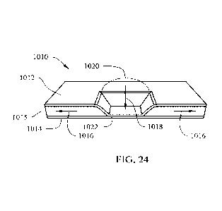
region of the subject battery). Such a low level would thus only generate a
temperature increase
.. of 0.01 C within such an 1-gram local region of battery, thus preventing
thermal runaway within
the target cell and thus overall battery.
[0102] Therefore, it is another significant advantage of the present
disclosure to provide
the battery a current collector that drastically limits the delivery time of a
current level applied
to the target current collector surface through a probe tip (in order to
controllably emulate the
effect of an internal manufacturing defect, a dendrite, or an external event
which causes an
internal short within the subject battery) to less than 1 second, preferably
less than 0.01 seconds,
more preferably less than 1 millisecond, and most preferably, perhaps, even
less than 100
microseconds, particularly for much larger currents. Of course, such a current
would be limited
to the internal voltage of the cell, which might be 5.0 V, or 4.5 V, or 4.2 V
or even less, such as
4.0 V or 3.8 V, but with a minimum of 2.0 V.
[0103] Such a novel current collector component is actually
counterintuitive to those typically
CA 03163083 2022-05-26
WO 2021/108119
PCT/US2020/059794
19
utilized and found within lithium (and other types) of batteries and energy
storage devices today.
Standard current collectors are provided are conductive metal structures, such
as aluminum
and/or copper panels of thicknesses that are thought to provide the necessary
strength to survive
the manufacturing process. The strength of these metals necessitates a
thickness that is far in
excess of the electrical needs of the cell. For example, the electrical needs
of the cell dictate a
metal thickness on the order of 500nm of Aluminum, while the thinnest solid
foil aluminum that
can survive the manufacturing process is around 10 p.m. It appears, however,
that such a belief
has actually been misunderstood, particularly since the thick panels prevalent
in today's energy
storage devices will actually support any current the typically low impedance
cell can deliver
.. when a short occurs and thus contribute greatly to runaway temperatures if
and when such a
situation occurs. Such a short may be caused, for example, by a dendritic
formation between the
anode and cathode. Such a malformation (whether caused at or during
manufacture or as a
result of long-term usage and thus potential degradation) may allow for
voltage to pass
unexpectedly from the anode to the cathode, thereby creating an increase in
current and
consequently in temperature at the location such occurs. Indeed, one potential
source of short
circuit causing defect are burrs that form on the edges of these thick typical
current collectors
when they are slit or cut with worn blades during repetitive manufacturing
processes of multiple
products (as is common nowadays). It has been repeatedly analyzed and
understood, however,
that the standard current collector materials merely exhibit a propensity to
create a durable
short circuit and allow for temperature increase, and further permitting the
current present
during such an occurrence to continue through the device, thus allowing for
unfettered generation
and movement, leaving no means to curtail the current and thus temperature
level from
increasing. This problem leads directly to runaway high temperature results;
without any
internal means to stop such a situation, the potential for fire generation and
ultimately device
immolation and destruction is typically imminent. Additionally, the current
pathway (charge
direction) of a standard current collector remains fairly static both before
and during a short
circuit event, basically exhibiting the same potential movement of electric
charge as expected
with movement from cathode to anode and then horizontally along the current
collector in a
specific direction. With a short circuit, however, this current pathway fails
to prevent or at least
curtail or delay such charge movement, allowing, in other words, for rapid
discharge in runaway
fashion throughout the battery itself. Coupled with the high temperature
associated with such
rapid discharge leads to the catastrophic issues (fires, explosions, etc.)
noted above.
CA 03163083 2022-05-26
WO 2021/108119
PCT/US2020/059794
[0104]
To the contrary, and, again, highly unexpected and counterintuitive to the
typical
structures and configurations of lithium batteries, at least, the utilization
of a current collector of
the instant disclosure results in an extremely high current density
measurement (due to the
reduced thickness of the conductive element) and prevention of charge movement
(e.g., no
5 charge direction) in the event of a short circuit. In other words, with
the particular structural
limitations accorded the disclosed current collector component herein, the
current density
increases to such a degree that the material is unable to remain intact and
fails by vaporizing.
[0105]
The total amount of energy necessary to cause this failure of the conductor is
low as
discussed above and results in very low temperatures generated from the event.
Combined with
10 the other structural considerations of such a current collector
component, namely the actual lack
of a dimensionally stable polymeric material in contact with such a conductive
material layer,
the conductive material oxidizes instantly at the charge point thereon,
leaving, for example,
aluminum or cupric oxide, both nonconductive materials. With such
instantaneous
nonconductive material generation, the short circuit charge appears to
dissipate as there is no
15 direction available for movement thereof. Thus, with the current
collector as now described,
an internal short circuit occurrence results in an immediate cessation of
current, effectively
utilizing the immediate high temperature result from such a short to generate
a barrier to further
charge movement. As such, the lack of further current throughout the body of
the energy
storage device (in relation to the short circuit, of course) mutes such an
undesirable event to
20 such a degree that the short is completely contained, no runaway current
or high temperature
result occurs thereafter, and, perhaps most importantly, the current collector
remains viable for
its initial and protective purposes as the localized nonconductive material
then present does not
cause any appreciable reduction in current flow when the energy storage device
(battery, etc.)
operates as intended.
Furthermore, the relatively small area of nonconductive material
generation leaves significant surface area, etc., on the current collector,
for further utilization
without any need for repair, replacement, or other remedial action. The need
to ensure such a
situation, which, of course, does not always occur, but without certain
precautions and
corrections, as now disclosed, the potential for such a high temperature
compromise and
destruction event actually remains far higher than is generally acceptable.
Thus, the entire
current collector, due to its instability under the conditions of a short
circuit, becomes a two-
dimensional electrical fuse, preventing the potentially disastrous high
currents associated with
CA 03163083 2022-05-26
WO 2021/108119
PCT/US2020/059794
21
short circuits by using the instantaneous effect of that high current to
destroy the ability of the
current collector to conduct current at the point of the short circuit.
[0106] Such advantages are permitted in relation to such a novel
resultant current collector
that may be provided, with similar end results, through a number of different
alternatives. In
any of these alternative configurations, such a current collector as described
herein functions
ostensibly as an internal fuse within a target energy storage device (e.g.,
lithium battery,
capacitor, etc.). In each instance (alternative), however, there is a current
collector including a
polymeric layer that is metalized on one or both sides thereof with at least
one metalized side in
contact with the anode or cathode of the target energy storage device. One
alternative then is
where the total thickness of the entire metalized (coated) polymeric substrate
of the current
collector is less than 20 microns, potentially preferably less than 15
microns, and potentially more
preferably less than 10 microns, all with a resistance measurement of less
than 1 ohm/square
potentially preferably less than 0.1 ohms/square, and potentially more
preferably less than 50
milli-ohms/square. Typical current collectors may exhibit these features but
do so at far higher
weight than those made with reinforcing polymeric substrates and without the
inherent safety
advantages of this presently disclosed variation. For example, a copper foil
at 10 microns thick
may weight 90 grams/m2. However, a copperized foil may weigh as little as 50
grams/m2, or
even as little as 30 gram/m2, or even less than 20 grams/m2, all while
delivering adequate
electrical performance required for the cell to function. In this alternative
structure, however,
the very thin component also allows for a short to react with the metal coat
and in relation to the
overall resistance levels to generate, with an excessively high temperature
due to a current
spike during such a short, a localized region of metal oxide that immediately
prevents any further
current movement therefrom.
[0107] Another possible alternative for such a novel current collector
is the provision of a
temperature dependent metal (or metalized) material that either shrinks from a
heat source during
a short or easily degrades at the specific material location into a
nonconductive material (such as
aluminum oxide from the aluminum current collector, as one example and as
alluded to above in
a different manner). In this way, the current collector becomes thermally
weak, in stark contrast
to the aluminum and copper current collectors that are used today, which are
quite thermally
stable to high temperatures. As a result, an alloy of a metal with a lower
inherent melting
temperature may degrade under lower shorting current densities, improving the
safety advantages
CA 03163083 2022-05-26
WO 2021/108119
PCT/US2020/059794
22
of the lithium-based energy device disclosed herein. Another alternative is to
manufacture the
current collector by coating a layer of conductive material, for example
copper or aluminum, on
fibers or films that exhibit relatively high shrinkage rates at relatively low
temperatures.
Examples of these include thermoplastic films with melt temperatures below 250
C, or even
200 C, and can include as non-limiting examples polyethylene terephthalate,
nylon, polyethylene
or polypropylene. Another possible manner of accomplishing such a result is to
manufacture a
current collector by coating a layer of conductive material, for example
copper or aluminum,
as above, on fibers or films that can swell or dissolve in electrolyte when
the materials are heated
to relatively high temperatures compared to the operating temperatures of the
cells, but low
compared to the temperatures that might cause thermal runaway. Examples of
such polymers
that can swell in lithium ion electrolytes include polyvinylidene fluoride and
poly acrylonitrile,
but there are others known to those with knowledge of the art. Yet another way
to accomplish
such an alternative internal electrical fuse generating process is to coat
onto a substrate a metal,
for example aluminum, that can oxidize under heat, at a total metal thickness
that is much lower
than usually used for lithium batteries. For example, a very thin aluminum
current collector as
used today may be 20 microns thick. A coating thickness of a total of less
than 5 microns would
break the circuit faster, and one less than 2 microns, or even less than 1
micron would break the
circuit even faster. Even still, another way to accomplish the break in
conductive pathway is to
provide a current collector with limited conductivity that will degrade in the
high current
densities that surround a short, similar to the degradation found today in
commercial fuses. This
could be accomplished by providing a current collector with a resistivity of
greater than 5
mOhm/square, or 10 mOhm/square, or potentially preferably greater than 20
mOhm/square, or,
a potentially more preferred level of greater than 50 mOhm/square. These
measurements could
be on one side, or on both sides of a material coated on both sides. The use
of current collectors
of different resistivities may further be selected differently for batteries
that are designed for
high power, which might use a relatively low resistance compared to cells
designed for lower
power and higher energy, and/or which might use a relatively high resistance.
Still another way
to accomplish the break in conductive pathway is to provide a current
collector that will oxidize
into a non-conductive material at temperatures that are far lower than
aluminum, thus allowing
the current collector to become inert in the area of the short before the
separator degrades.
Certain alloys of aluminum will oxidize faster than aluminum itself, and these
alloys would cause
the conductive pathway to deteriorate faster or at a lower temperature. As
possible alternatives,
CA 03163083 2022-05-26
WO 2021/108119
PCT/US2020/059794
23
there may be employed any type of metal in such a thin layer capacity and that
exhibits electrical
conductivity, including, without limitation, gold, silver, vanadium, rubidium,
iridium, indium,
platinum, and others (basically, with a very thin layer, the costs associated
with such metal usage
may be reduced drastically without sacrificing conductivity and yet still
allowing for the
.. protections from thermal runaway potentials during a short circuit or like
event). As well, layers
of different metals may be employed or even discrete regions of metal
deposited within or as
separate layer components may be utilized. Certainly, too, one side of such a
coated current
collector substrate may include different metal species from the opposing
side, and may also
have different layer thicknesses in comparison, as well.
[0108] One way to improve the electrical properties of the cell would be to
ensure that a
coated current collector includes two conductive coated sides, ostensibly
allowing for
conductivity from the coating on one side to the coating on the other side.
Such a result is not
possible for a non- coated polymer film, for instance. However, it has been
realized that such a
two-sided conductivity throughput can be achieved by, as one non-limiting
example, a nonwoven
including a certain percentage of conducting fibers, or a nonwoven loaded with
conductive
materials, or a nonwoven made from a conductive material (such as carbon
fibers or metal
fibers), or, as noted above, a nonwoven containing fibers coated with a
conductive material
(such as fibers with a metal coating on the surface). Another type of novel
thin current collector
material exhibiting top to bottom conductivity may be a film that has been
made conductive,
such as through the utilization of an inherently conductive material (such as,
for example,
conductive polymers such as poly acetylene, polyaniline, or
polyvinylpyrrolidone), or via loading
with a conductive material (such as graphite or graphene or metal particles or
fibers) during or
after film manufacture. Additionally, another possible two-sided thin current
collector material
is a polymer substrate having small perforated holes with sides coated with
metal (aluminum or
copper) during the metallization process. Such a conductivity result from one
side to the other
side would not need to be as conductive as the conductive coatings.
[0109] Thus, such alternative configurations garnering ostensibly the
same current collector
results and physical properties include a) wherein the total thickness of the
coated polymeric
substrate is less than 20 microns with resistance less than 1 ohm/square, b)
the collector
comprising a conductive material coated on a substrate comprising polymeric
material, wherein
the polymeric material exhibits heat shrinkage at 225 C of at least 5%, c)
wherein the collector
CA 03163083 2022-05-26
WO 2021/108119
PCT/US2020/059794
24
metalized polymeric material swells in the electrolyte of the battery, such
swelling increasing as
the polymeric material is heated, d) wherein the collector conductive material
total thickness is
less than 5 microns when applied to a polymeric substrate, e) wherein the
conductivity of the
current collector is between 10 mOhm/square and 1 ohm/square, and f) wherein
the metalized
.. polymeric substrate of the collector exhibits at most 60% porosity. The
utilization of any of
these alternative configurations within an energy storage device with a
separator exhibiting a
heat shrinkage of less than 5% after 1 hour at 225 C would also be within the
purview of this
disclosure. The overall utilization (method of use) of this type of energy
storage device (battery,
capacitor, etc.) is also encompassed herein.
[0110] While the primary advantage of this invention is enhanced safety for
the cell, there are
other advantages, as alluded to above, including reduced weight of the overall
energy storage
device through a reduced amount of metal weight in relation to such current
collector
components. Again, it is completely counterintuitive to utilize thin metalized
coated polymeric
layers, particularly of low dimensionally stable characteristics, for current
collectors within such
battery articles. The present mindset within this industry remains the thought
that greater
amounts of actual metal and/or insulator components are needed to effectuate
the desired
protective results (particularly from potential short circuit events). It has
now been unexpectedly
realized that not only is such a paradigm incorrect, but the effective remedy
to short circuiting
problems within lithium batteries, etc., is to reduce the amount of metal
rather than increase and
couple the same with thermally unstable base layers. Thus, it has been not
only realized, again,
highly unexpectedly, that thin metal layers with such unstable base layers
provide the ability to
combat and effectively stop discharge events during short circuits, the
overall effect is not only
this far safer and more reliable result, but a significantly lower overall
weight and volume of
such component parts. Thus, the unexpected benefits of improved properties
with lowered
.. weight and volume requirements within energy storage products (batteries,
etc.), accords far
more to the industry than initially understood.
[0111] As a further explanation, aluminum, at a density of 2.7 g/cm3, at
20 microns thick
would weigh 54 g/m2. However, the same metal coated at 1 micron on a 10-micron
thick
polypropylene film (density 0.9 g/cm3) would weigh 11.7 g/m2. This current
collector reduction
.. in weight can reduce the weight of the entire target energy storage device
(e.g., battery),increasing
mobility, increasing fuel mileage or electric range, and in general enhance
the value of mobile
CA 03163083 2022-05-26
WO 2021/108119
PCT/US2020/059794
electric applications.
[0112] Additionally, because of the high strength of films, the above
example can also be
made thinner, a total thickness of 11 microns compared to 20 microns, for
example, again
reducing the volume of the cell, thereby effectively increasing the energy
density. In this way, a
5 current collector of less than 15 microns, preferably less than 12, more
preferably less than 10,
and most preferably less than 8 microns total thickness, can be made and
utilized for such a
purpose and function. With the bulk resistivity of aluminum at 2.7 x10⁻⁸ ohm-m
and of copper
at 1.68 x10⁻⁸ ohm-m, a thin coating can be made with less than 1 ohm/square,
or less than 0.5
ohms/square, or even less than 0.1 ohms/square, or less than 0.05 ohms/square.
The thickness of
10 .. these conductive coatings could be less than 5 microns, preferably than3
microns, more
preferably less than 2 microns, potentially most preferably even less than 1
micron. It is
extremely counterintuitive, when standard materials of general use in the
market contain 10
microns or more of metal, that suitable performance could be obtained using
much less metal.
Indeed, most of the metal present in typical storage devices is included to
give suitable
15 .. mechanical properties for high speed and automated processing. It is one
of the advantages of
this invention to use a much lower density polymer material to provide the
mechanical properties,
allowing the metal thickness to be reduced to a level at which the safety of
the cell is improved
because of the inability of the current collector to support dangerously high
current densities
that result from internal electrical shorts and result in thermal runaway,
smoke and fire.
20 [0113] Additionally, these conductive layers can be made by
multiple layers. For example, a
layer of aluminum may be a base layer, coated by a thin layer of copper. In
this way, the bulk
conductivity can be provided by the aluminum, which is light, in expensive and
can easily be
deposited by vapor phase deposition techniques. The copper can provide
additional conductivity
and passivation to the anode, while not adding significant additional cost and
weight. This
25 example is given merely to illustrate and experts in the art could
provide many other multilayer
conductive structures, any of which are excellent examples of this invention.
[0114] These thin metal coatings will in general result in higher
resistance than in an
aluminum or copper current collector of normal practice, providing a
distinguishing feature of
this invention in comparison. Such novel suitable current collectors can be
made at greater than
10 mOhm/square, preferably greater than 20 mOhm/square, more preferably
greater than 50
mOhm/square, and potentially most preferably even greater than 100
mOhm/square.
CA 03163083 2022-05-26
WO 2021/108119
PCT/US2020/059794
26
[0115] Additionally, cells made with the thermally weak current
collectors described above
could be made even more safe if the separator has a high thermal stability,
such as potentially
exhibiting low shrinkage at high temperatures, including less than 5%
shrinkage after exposure
to a temperature of 200 C for 1 hour, preferably after an exposure of 250 C
for one hour, and
potentially more preferably after an exposure to a temperature of 300 C for
one hour. Existing
separators are made from polyethylene with a melt temperature of 138 C and
from
polypropylene with a melt temperature of 164 C. These materials show
shrinkage of >50% at
150 C, as shown in Figure 2; such a result is far too high for utilization
with a thin current
collector as now described herein. To remedy such a problem, it has been
realized that the
utilization of certain separators that shrink less than 50% at 150 C, or even
less than 30%, or
less than 10%, as measured under NASA TM-2010-216099 section 3.5 are
necessary. Even
ceramic coated separators show significant shrinkage at relatively modest
temperatures, either
breaking entirely or shrinking to more than 20% at 180 C. It is thus
desirable to utilize a
separator that does not break during the test, nor shrink to more than 20% at
an exposure of 180
C (at least), more preferably more than 10%, when measured under the same test
standard. The
most preferred embodiment would be to utilize a separator that shrinks less
than 10% when
exposed to a temperature of 200 C, or 250 C, or even 300 C.
[0116] For any of these metalized substrates, it is desirable to have a
low thickness to
facilitate increase the energy density of the cell. Any means can be used to
obtain such thickness,
including calendering, compressing, hot pressing, or even ablating material
from the surface in a
way that reduces total thickness. These thickness-reducing processes could be
done before or
after metallization. Thus, it is desirable to have a total thickness of the
metalized substrate of
less than 25 microns, preferably less than 20 microns, more preferably less
than 16 microns, and
potentially most preferably less than 14 microns. Commercial polyester films
have been realized
with thicknesses of at most 3 microns, and even lower at 1.2 microns. These
types could serve
as suitable substrates and allow the total thickness of the current collector
to be less than 10
microns, preferably less than 6 microns, and more preferably less than 4
microns. Such ultra-
thin current collectors (with proper conductivity as described above and
throughout) may allow
much higher energy density with improved safety performance, a result that has
heretofore gone
unexplored.
[0117] It is also desirable to have low weight for these metalized
substrates. This could be
CA 03163083 2022-05-26
WO 2021/108119
PCT/US2020/059794
27
achieved by the use of low-density polymer materials such as polyolefins or
other low-density
polymers including polyethylene, polypropylene, and polymethylpentene, as
merely examples. It
could also be achieved by having an open pore structure in the substrate or
even through
utilization of low basis weight substrates. Thus, the density of the polymer
used in the substrate
material could be less than 1.4 g/cm3, preferably less than 1.2 g/cm3, and
potentially more
preferably less than 1.0 g/cm3. Also, the areal density of the substrate
material could be less than
20 g/m2, preferably less than 16 g/m2, and potentially most preferably less
than 14 g/m2.
Additionally, the areal density of the metal coated polymer substrate material
could be less than
40 g/m2, preferably less than 30 g/m2, more preferably less than 25 g/m2, and
potentially most
preferably less than 20 g/m2.
[0118] Low weight can also be achieved with a porous polymer substrate.
However, the
porosity must not be too high for these materials, as such would result in low
strength and high
thickness, effectively defeating the purpose of the goals involved. Thus, such
base materials
would exhibit porosity lower than about 60%, preferably lower than 50%, and
potentially more
preferably lower than 40%. Since solid materials can be used for this type of
metal coated
current collector, there is no lower limit to the porosity.
[0119] High strength is required to enable the materials to be processed
at high speeds into
batteries. This can be achieved by the use of elongated polymers, either from
drawn fibers or
from uniaxially or biaxially drawn films.
[0120] As presented below in the accompanying drawings the descriptions
thereof, an energy
storage device, whether a battery, a capacitor, a supercapacitor and the like,
is manufactured and
thus provided in accordance with the disclosure wherein at least one current
collector that
exhibits the properties associated with no appreciable current movement after
a short is
contacting a cathode, an anode, or two separate current collectors contacting
both, and a separator
and electrolytes, are all present and sealed within a standard (suitable)
energy storage device
container, is provided. The cathode, anode, container, electrolytes, and in
some situations, the
separator, components are all standard, for the most part. The current
collector utilized herewith
and herein, however, is, as disclosed, not only new and unexplored within this
art, but
counterintuitive as an actual energy storage device component. Such is, again,
described in
greater detail below.
[0121] As noted above, in order to reduce the chances, if not totally
prevent, thermal runaway
CA 03163083 2022-05-26
WO 2021/108119
PCT/US2020/059794
28
within a battery cell (particularly a lithium ion rechargeable type, but
others are possible as well,
of course), there is needed a means to specifically cause any short circuit
therein to basically
exist within a short period of time, with reduced residence time within or on
the subject current
collector, and ultimately exhibit a resultant energy level of de minimis joule
levels (i.e., less
than 10, preferably less than 1, and most preferably less than 0.01). In such
a situation, then,
and as alluded to earlier, the electrical pathway from anode to cathode, and
through the separator,
with the thin conductive current collector in place, and organic flammable
electrolyte present, it
has been observed that the low-weight, thin current collector allows for such
a desirable result,
particularly in terms of dissipation of rogue charges at the collector surface
and no appreciable
temperature increase such that ignition of the electrolyte component would be
imminent.
Surprisingly, and without being bound to any specific scientific explanation
or theory, it is
believed that the conductive nature of the thin current collector material
allows for short circuit
electrical charges to merely reach the thin conductive current collector and
immediately create a
short duration high-energy event that reacts between the metal at the current
collector surface
with the electrical charge itself, thereby creating a metal oxide to form at
that specific point on
the current collector surface. The metal oxide provides insulation to further
electrical activity
and current applied dissipates instantaneously, leaving a potential
deformation within the
collector itself, but with the aforementioned metal oxide present to protect
from any further
electrical charge activity at that specific location. Thus, the remaining
current collector is intact
.. and can provide the same capability as before, thus further providing such
protections to any
more potential short circuits or like phenomena. In the case of thermal
runaway in prior art
battery products, the anode, cathode, current collectors and separator
comprise the electrical
pathway which generate heat and provide the spark to ignite the cell in
reaction to a short
circuit, as an example. The further presence of ion transporting flammable
electrolytes thus
allows for the effective dangers with high temperature results associated with
such unexpected
electrical charges. In essence, the heat generated at the prior art current
collector causes the
initial electrochemical reactions within the electrolyte materials, leading,
ultimately to the
uncontrolled ignition of the electrolyte materials themselves. Thus, the
disclosed inventive
current collector herein particularly valuable when utilized within battery
cells including such
flammable electrolytes. As examples, then, such electrolytes generally include
organic solvents,
such as carbonates, including propylene carbonate, ethylene carbonate, ethyl
methyl carbonate, di
ethyl carbonate, and di methyl carbonate, and others. These electrolytes are
usually present as
CA 03163083 2022-05-26
WO 2021/108119
PCT/US2020/059794
29
mixtures of the above materials, and perhaps with other solvent materials
including additives of
various types. These electrolytes also have a lithium salt component, an
example of which is
lithium hexafluorophosphate, LiPF6. Such electrolytes are preferred within the
battery industry,
but, as noted, do potentially contribute to dangerous situations. Again, this
inventive current
collector in association with other battery components remedies these concerns
significantly and
surprisingly.
[0122] One way that this current collector will exhibit its usefulness
is in the following test.
A current source with both voltage and current limits can be set to a voltage
limit similar to the
operating voltage of the energy storage device in question. The current can
then be adjusted, and
the current collector tested fewer than two configurations. In the first, a
short strip of the current
collector of known width is contacted through two metal connectors that
contact the entire width
of the sample. The current limit of the current source can be raised to see if
there is a limit to the
ability of the material to carry current, which can be measured as the total
current divided by the
width, achieving a result in A/cm, herein designated as the horizontal current
density. The
second configuration would be to contact the ground of the current source to
one of the full width
metal contacts, and then touch the tip of the probe, approximately 0.25 mm2,
to a place along the
strip of the current collector. If the current is too high, it will burn out
the local area, and no
current will flow. If the current is not too high for the current collector,
then the full current up to
the limit of the current source will flow. The result is a limit of current in
A/mm2, herein
designated as the vertical current density. In this way, a current collector
which can reach a high
current under both configurations would be similar to the prior art, and a
current collector which
could support the horizontal current when contacted under full width, but
would not support a
similar vertical current under point contact would be an example of the
invention herein
described.
[0123] For example, it may be desirable for a current collector to be able
to support horizontal
current density 0.1 A/cm, or 0.5 A/cm, or 1 A/cm or 2 A/cm or even 5 A/cm. And
for a current
collector that could support a horizontal current density as above, it would
be desirable not to
support a vertical current density of 0.1 A/mm2, or 0.5 A/mm2, or 1 A/mm2 or 2
A/mm2 or even
5 A/mm2.
[0124] As alluded to above, there is also generally present within lithium
ion battery cells a
tab weld to join the internal components, particularly the current collectors,
together to connect
CA 03163083 2022-05-26
WO 2021/108119
PCT/US2020/059794
to a tab lead for transfer of charge to an external source. In this situation,
with the current
collectors of extremely thin types, it is paramount such a tab lead
effectively contact the internal
metalized film collectors and remain sufficiently in place to contact an
external source as well.
Additionally, due to the effectiveness of the aforementioned and unexpectedly
good metalized
5 thin film current collectors to permit the needed operations of the
battery cell itself, as well as
the ability to provide the internal fuse characteristics to prevent runaway
current during a
possible problem (dendrite formation, etc.), such a tab must not exhibit any
degree of
displacement or ineffectiveness to combat the same potential runaway charge
issues themselves.
In other words, the effectiveness of the internal fuse results must not be
undone or compromised
10 by tab issues. Surprisingly, it has been determined that such needed
characteristics are
permissible with such tab components.
[0125] To that level, then, it was realized that the metalized thin film
collectors actually allow
for an effective and strong weld of the tab thereto and with the ability to
actually allow for
conductance at both film sides. The tab itself is actually thicker than each
individual current
15 collector and when placed in contact with one another the weld may be
undertaken to a depth
that is partially through the tab material in relation to the shape and depth
of the weld itself.
The surprising result, however, is that the weld may actually pass through the
tab in a thin
"stream" or like formation, thus allowing for conductance through such a weld
material to the
tab. In this manner, the limited, though effective, conduction path is
generated in order to not
20 only allow for the needed conductance at the weld location to the tab
(and then out of the battery
cell casing to an external source), but also there is provided a means to
limit the actual amperage
and temperature generated by such a conductive flow at each weld location.
Such a result
allows for the aforementioned control of runaway conductivity from the
metalized film current
collectors should a short (dendrite formation, etc.) occur since the
electrical charge will stop at
25 the actual current collector surface and no other pathway for a runaway
charge is provided. The
welds may thus be provided along the length of the tab component running along
the current
collector with as many as five, as one example, spaced uniformly from one
another, thus allowing
for effective conductivity from the foil collector(s) to the tab through the
battery casing to the
external source. The limited number of welds thus reduces, as well, the number
of possible
30 runaway charge sites, albeit with each exhibiting limited amperage, but
with multiples such
levels show increases in some situations, certainly. However, for high power
or high current
CA 03163083 2022-05-26
WO 2021/108119
PCT/US2020/059794
31
batteries, the number of welds per tab can be increased to accommodate the
high amount of
current needed for the battery to be effective in its application. In this
case, it is possible to
require a larger number of welds, potentially as many as 10, or 20, or even 50
welds per tab. In
rare circumstances in very high power or very high current cells, even more
than 50 welds may be
.. necessary. The welds provide a base strength, additionally, to prevent
movement of the tab
during utilization. Stability and rigidity and needed to ensure proper
operation of the battery
overall. The limited welds do provide a certain level of reliability in this
respect, while the
addition of pull tape thereover as applied to the current collector films also
aids in protecting
from such potential problems as well.
[0126] In effect, the metalized thin film current collectors are
unexpectedly good for the
prevention of runaway charges during a short. However, the need for tab leads
in sufficient
contact with such collectors in order to allow for effective conductivity
external the battery
cell requires a structural situation that allows for such metalized thin
current collector film
utilization with standard tab components. As noted above, the ability to
determine proper
dimensions of both current collector film(s) and tabs with suitable welds for
effective attachment
and contact for electrical current to pass through effectively for battery
operation, while still
exhibiting the proper low potential for runaway charge has proven difficult,
particularly in view
of the specific and accepted thick monolithic current collector components of
the state of the
art today. This unexpectedly effective result, particularly with the tab
contact and pull strength
.. characteristics determined as noted above, accords a full lithium ion
battery that may be provided
with reduced weight or greater internal capacity for other components without
sacrificing battery
power generation capability while simultaneously providing complete protection
from runaway
charges during short circuit events.
[0127] Additionally, of importance is the ability to utilize heretofore
unexplored welding
operations and methodologies to provide effective and reliable connections
between such
metallic conductors (again, tabs) and electrodes within thin metalized film
current collector
containing power generating cells. The need for such effective connections to
not only impart
safety aspects to such cells (with the thin film current collectors described
herein) but the
important conductivity from electrode to the outside world (in other words to
allow for proper
and effective utilization of such a power generating cell, i.e., battery,
capacitor, and the like).
Such power cells, which may be configured and structured with containers noted
above, as
CA 03163083 2022-05-26
WO 2021/108119
PCT/US2020/059794
32
well as, without limitation, metalized plastic bags, metal cans, and
rigid/semi-rigid plastic
enclosures, would, again, exhibit much improved potential for thermal runaway
with metalized
thin film current collectors. The proper connection between such power cells
and external
contacts is thus of great necessity for actual functional purposes,
particularly with the
complexities of providing such reliable and secure connections with thin film
materials.
[0128] To that end, and, again, in addition to the descriptions and
disclosures of metalized
thin film metalized current collectors and general tab possibilities above, it
has been realized that
certain weld configurations and actual welding tools provide for such
beneficial and surprisingly
effective tab-electrode connections for such unique power cell structures.
Particularly important
battery (power cell) types include, without limitation, pouch, cylinder,
prismatic and jelly roll
structures as these types of cells are most prevalent within certain
industries and allow for greater
versatility for subject devices, as well.
[0129] The dynamics of such unique weld methods and operations take into
effect the
metalized thin film current collector in a specific configuration,
particularly one with at least one
layer of metalized film having at least two metallization layers separated by
a polymer substrate.
The weld must then be imparted to such a structure such that the divot of the
weld extrudes
through from the first metalized layer through the polymer substrate and to
the second metalized
layer. In this manner, the utilization of a proper weld anvil creates a
certain three-dimensional
divot within a subject region of the current collector such that the top
(first) metalized layer
becomes contacted with the lower (second) metalized layer, the polymer
substrate moves in
opposing relation to the weld divot and within the confines of the two
metalized layers, and the
resultant welded structure retains the top and lower metalized layers
separated by the polymer
substrate outside of the welded region. With this weld result, the ability to
create such a
connection between the current collector and a tab structure is thus available
without losing the
necessary safety benefits of the thin film current collector itself within the
target cell. Of course,
this may also apply to a film that is metalized on only one side, and
electrical contact is desired
to a component on the other side of the polymer substrate, such as a tab or
the metalized side
of a subsequent metalized thin film current collector. In this case, the weld
must then be
imparted such that the divot of the weld extrudes through from the metalized
layer through the
polymer substrate to the component with which electrical contact is desired.
[0130] The inclusion of a tab material within a weld thus allows for the
weld anvil to press
CA 03163083 2022-05-26
WO 2021/108119
PCT/US2020/059794
33
through the tab and move the current collector (again, thin film of at least
two metalized layers
separated by a polymer substrate) in the same manner, thus creating a divot
within the tab and
current collector simultaneously for connection capabilities between both
structure to form a
composite for conductivity purposes. Such tab weld attachment may be
undertaken on either of
the top or bottom of such a thin film current collector as well, thereby
allowing for the tab to
basically connect with the top and bottom metalized layers simultaneously in
either manner.
Thus, with the further inclusion of an electrode (coating or otherwise) on the
current collector,
the ability to properly and effectively connect the entire power cell
structure (electrode/current
collector, at least) to the target tab for the further provision of
conductivity external of such an
improved safety (thin film current collector) power cell is achieved. This
ability to suitable and
effectively provide conductivity from the current collector (both metalized
film layers)
simultaneously to such a tab for external power transmission allows for the
overall functionality
and, for that matter, proper utilization of such a safe battery device that
has, again, heretofore
been unexplored. Without the effective weld operation for both metalized film
layers of the
base current collector, such a power transfer would be hindered, basically. Of
course, as alluded
to above, the current collector may be of multiple layered structures of a
single polymer substrate
separating two metalized layers in each such structure (in other words,
repeating units of thin
film polymer substrate with top and bottom metalized films as desired; at
least one such base
structure may be present with any number layered on one another up to about 12-
15 or more,
depending on the end use thereof Such multiple base structure power cells
would require the
same needed weld connection(s) with at least one base substrate/top and bottom
metalized film
structures for functionality of the target power cell. The number of layers of
metalized film that
are welded together may be 15, or may be higher, as many as 25, or even 50 in
a single stack. If
the number gets too high, the distance that the metalized film is extruded to
make contacts with
the layers below may become very high. Thus, the maximum number of layers in a
stack may be
less than 250, or preferably less than 100, or even more preferably less than
50.
[0131] More than one weld divot may be employed for such connection purposes
between
the thin film current collector (again, polymer substrate with top and bottom
metalized films,
and at least one such structure present) and the tab. Such welds may be
provided within a
small region of the current collector (and thus tab) or may be provided as
repeated divots of the
same three-dimensional structure in patterns thereof or possibly with
different three-dimensional
CA 03163083 2022-05-26
WO 2021/108119
PCT/US2020/059794
34
structures in patterned or random configurations. Furthermore, random
configurations of the
same three-dimensional weld structures may be employed as well. The importance
of such weld
divots is to impart, again, the proper and effective connections between the
tab and the current
collector while allowing for the thin film to retain the needed safety aspects
associated thereof
(reduce the propensity of thermal runaway) while still retaining the proper
ability to transfer
charge and thus conductivity external to the power cell itself. Such weld
structures allow, again,
for three-dimensional structures that allow for limited regions of the tab and
current collector to
contact with a certain uniformity of displacement of polymer substrate
allowing for the top and
bottom metalized film layers to contact one another with the tab as well
manipulated for contact
with such a top and bottom metalized layer contact. Multiple divots allow for
increased
conductivity on demand, as well as increased surface area connections for more
reliable
attachment between tab and current collector, as well. Such three-dimensional
weld divots may
be made from any number of weld anvil structures, including, without
limitation, rectangular
(linear) three-dimensional anvils, spherical (or semi-spherical), truncated
pyramid (with a square
bottom and a smaller square top), rounded pyramid (with curved edges at the
top thereof) , and
the like. Such structures impart divots that will allow for the top metalized
layer (or bottom
depending on the location of the actual weld, whether on the top or bottom of
the current
collector) to deform downwardly without breaking the film and contact for a
certain area with
the bottom metalized layer, while the polymer substrate displaces but remains
in contact to the
.. manipulated metalized film layers to provide a force against such a
manipulated region thereof
for dimensional stability subsequent to such a weld operation. As noted above,
such welds may
be provided singly within such a tab/current collector composite structure, or
may be applied in
multiples for increased surface area contact between the two composite
components, either
uniformly, randomly, entirely (over a certain region), or sparsely (within a
region). Again, the
ability to impart the safety aspects of the current collector structure within
a target power cell
while allow for proper and effective connection with a tab for conductivity
purposes is paramount
in this situation. The thin film collectors can thus, unexpectedly, be
utilized with such resultant
effectiveness in this weld operation with the tab to great effect.
[0132] Such a welding operation may utilize ultrasonic, heat application
(through an anvil, for
instance), or pressure application (again, through the utilization of an
anvil). Such applications
may include the utilization of a single anvil or multiple anvils
simultaneously within a grid that
CA 03163083 2022-05-26
WO 2021/108119
PCT/US2020/059794
applies to and over a certain region of the tab and current
collector/electrode bodies, as well (as
noted above). Such welding capabilities thus allow for a number of other
beneficial opportunities
that have not been explored in the past. These include the potential for a
configuration of
multiple current collectors and multiple tabs, all welded together, either
entirely or separately. A
5 single tab may be connected through welding to multiple layers of current
collectors, as well,
allowing for the connections of such top and bottom metalized layers within
such multi-layer
structures (at least two, and any number up to, for instance, 25). Also, a
staggered configuration
of current collectors and tabs may be employed, if desired, without
compromising safety or
power transfer, as well. Such an electrode tab may have an expanded region to
allow more welds
10 for, again, greater surface area for conductivity and/or connection
purposes. Additionally, the
tab/electrode connection may be in combination with a narrowed region of tab
to provide a "built
in" cell fuse. Such a cell fuse may impart the ability, as well, to thereby
increase the safety
aspects to an even greater degree. Additional metal layers may be inserted
between the current
collector film layers, as well, to aid in the weld capabilities between such
film stacks (particularly
15 with multiple layers present, again, up to about 25).
[0133] Furthermore, as it concerns the tab itself (or electrical
connector, as it is also referred
to), such a component is, as noted above, welded to the electrode and
subsequently connected
to either other cell components (within a container), or attached to (and
possibly through) a
target cell casing, thereby functioning as an external electrode for
connection with an external
20 device (to transfer power thereto, in other words).
[0134] As alluded to above, welding operations and processes may be
undertaken on the top
(tab side) or bottom (current collector film side) of the target composite
cell structure. In such
situations, welds may be from the tab side (through the utilization of a
moving horn device
thereon such a surface), with the anvil (non-moving) pressed on the film side
(as noted above).
25 The opposite may be employed, however, with the anvil pressed into the
tab with a moving horn
underneath on the film side (to provide a smooth structure for the anvil to
press against,
ultimately). In either situation, the ability to impart the desired weld divot
for connection and
adherence purposes is permitted in relation to the thin metalized current
collector for such a
safe, reliable and effective connection externally through the tab.
30 [0135] Furthermore, the ability to provide further beneficial
welding capabilities has been
realized in relation to weld stack configurations heretofore unexplored,
again, within any thin
CA 03163083 2022-05-26
WO 2021/108119
PCT/US2020/059794
36
film current collector situations. For instance, a single tab may be employed
with at least one
and up to about, without any limitation, 25 metalized film layers. Conversely,
perhaps, multiple
tabs with from one to about 25 metalized film layers may be utilized with tabs
present, as one
non-limiting possibility, at the top and bottom of the metalized film layer
stack. Alternatively,
then, such multiple tabs may also be interspersed throughout the metalized
film layer (current
collector) stack, uniformly or sparsely, as needed and/or desired. This allows
for a number of
different results and possibilities for power generation and transfer with
safe (low thermal
runaway propensity, again) cells.
[0136]
Additionally, then a single tab may be utilized that is sufficient in length
to fold over
and around a thin film current collector (or multi-layers thereof) and
basically welded not only to
the thin film collector(s), but to itself (acting like a clamp around the
collector(s), in effect.
[0137]
As mentioned above, the utilization of multiple welds aids in providing
sufficient
connection for overall strength to the composite generated thereby as well as
increased
conductivity potential from the power cell externally through the tab. The
number of welds
used may be numbered to achieve a maximum current for the cell beyond which
the welds will
fail and break connection to the tab. Such welding, in any number, as desired,
may be applied
on either electrode (anode or cathode) alone, or on both electrodes
simultaneously in identical
or different numbers, again, as desired.
[0138]
In terms of such welding capabilities, there is also the potential (and, at
times, need)
to ensure such connections between current collector/electrode and tab are
reinforced beyond
the welds themselves. The possibility of detachment between such components
due to weakened
welds may compromise the overall power cell capabilities, in other words. To
further bolster and
enhance the power generation and transfer benefits thereof such a safe (thin
current collector)
structure, tape, clamp, and possible combinations thereof, may be employed to
supplement the
welds themselves.
[0139]
Such lithium ion battery thin films may require certain unique processing
steps due to
their unique qualities. However, many processing steps that are well known in
the art may also
be employed. In general, the process to produce a lithium ion battery with the
inventive films
comprises the steps of:
a. Providing an electrode having at least one metalized substrate with a
coating of an ion
storage material;
CA 03163083 2022-05-26
WO 2021/108119
PCT/US2020/059794
37
b. Providing a counterelectrode;
c. Layering said electrode and counterelectrode opposite each other with a
separator
component interposed between said electrode and said counterelectrode;
d. Providing a package material including an electrical contact component,
wherein
said contact includes a portion present internally within said package
material
and a portion present external to said package material;
e. Electrically connecting said electrical contact with said metalized
substrate;
f. Introducing at least one liquid electrolyte with ions internally within
said package
material; and
g. Sealing said package material.
[0140] The metalized substrate can be any substrate as described within
this disclosure.
[0141] The ion storage material can for example be a cathode or anode
material for lithium
ion batteries, as are well known in the art. Cathode materials may include
lithium cobalt oxide
LiCo02, lithium iron phosphate LiFePO4, lithium manganese oxide LiMn204,
lithium nickel
manganese cobalt oxide LiNixMnyCoz02, lithium nickel cobalt aluminum oxide
LiNixCoyAlz02,
or mixtures of the above or others as are known in the art. Anode materials
may include
graphite, lithium titanate Li4Ti5012, hard carbon, tin, silicon or mixtures
thereof or others as are
known in the art. In addition, the ion storage material could include those
used in other energy
storage devices, such as supercapacitors. In such supercapacitors, the ion
storage materials will
include activated carbon, activated carbon fibers, carbide-derived carbon,
carbon aerogel,
graphite, graphene, graphene, and carbon nanotubes.
[0142] The coating process can be any coating process that is generally
known in the art.
Knife- over-roll and slot die are commonly used coating processes for lithium
ion batteries, but
others may be used as well, including electrolyses plating. In the coating
process, the ion storage
.. material is in general mixed with other materials, including binders such
as polyvinylidene
fluoride or carboxymethyl cellulose, or other film-forming polymers. Other
additives to the
mixture include carbon black and other conducting additives.
[0143] Counterelectrodes include other electrode materials that have
different electrochemical
potentials from the ion storage materials. In general, if the ion storage
material is a lithium ion
anode material, then the counterelectrode would be made form a lithium ion
cathode material. In
the case where the ion storage material is a lithium ion cathode material,
then the
CA 03163083 2022-05-26
WO 2021/108119
PCT/US2020/059794
38
counterelectrode might be a lithium ion anode material. In the case where the
ion storage
material is a supercapacitor material, the counterelectrode can be made from
either a
supercapacitor material, or in some cases from a lithium ion anode or lithium
ion cathode
material. In each case, the counterelectrode would include an ion storage
material coated on a
current collector material, which could be a metal foil, or a metalized film
such as in this
invention.
[0144] In the layering process, the inventive electrode is layered with
the counterelectrode
with the electrode materials facing each other and a porous separator between
them. As is
commonly known in the art, the electrodes may be coated on both sides, and a
stack of electrodes
formed with the inventive electrode and counterelectrodes alternating with a
separator between
each layer. Alternatively, as is also known in the art, strips of electrode
materials may be stacked
as above, and then wound into a cylinder.
[0145] Packaging materials may include hard packages such as cans for
cylindrical cells,
flattened hard cases or polymer pouches. In each case, there must be two means
of making
electrical contact through the case that can be held at different voltages and
can conduct current.
In some instances, a portion of the case itself forms one means, while another
is a different
portion of the case that is electrically isolated from the first portion. In
other instances, the case
may be nonconducting, but allow two metal conductors to protrude through the
case, often
referred to as tabs.
[0146] Connecting the means to make electrical contact with the metalized
substrate can
include commonly used methods, such as welding, taping, clamping, stapling,
riveting, or other
mechanical means. Because the metal of the metalized substrate can be very
thin, in order to
enable an interface that allows for high current flow, a face-to-face contact
is generally required,
giving high surface area between the means of making electrical contact
through the case and
the metalized substrate. To carry sufficient current, this surface area should
be higher than 1
square millimeter (10-12 square meters) but may need to be higher than 3
square millimeters, or
even 5 square millimeters or more preferably 10 square millimeters.
[0147] Of course, in addition to face-to-face contact, this weld may
include contact by
extruding the thin metal layer through the plastic layer to contact metal that
was previously on the
other side of said plastic layer, which may be in the form of divots created
through ultrasonic
welding or other method of welding.
CA 03163083 2022-05-26
WO 2021/108119
PCT/US2020/059794
39
[0148] The liquid electrolyte is typically a combination/mixture of a
polar solvent and a
lithium salt. Commonly used polar solvents include, as noted above, propylene
carbonate,
ethylene carbonate, dimethyl carbonate, diethyl carbonate, but other polar
solvents, including
ionic liquids or even water may be used. Lithium salts commonly utilized
within this industry
include, without limitation, LiPF6, LiPF4, LiBF4, LiC104 and others. The
electrolyte may also
contain additives as are known in the art. In many cases, the electrolytes can
be flammable, in
which the safety features of the inventive metalized substrate current
collectors can be
advantageous preventing dangerous thermal runaway events which result in fire
and damage
both to the cell and external to the cell.
[0149] The following descriptions and examples are merely representations
of potential
embodiments of the present disclosure. The scope of such a disclosure and the
breadth thereof in
terms of claims following below would be well understood by the ordinarily
skilled artisan within
this area.
[0150] As noted above, the present disclosure is a major shift and is
counterintuitive from all
prior understandings and remedies undertaken within the lithium battery (and
other energy
storage device) industry. To the contrary, the novel devices described herein
provide a number of
beneficial results and properties that have heretofore been unexplored, not to
mention
unexpected, within this area. Initially, though, as comparisons, it is
important to note the stark
differences involved between prior devices and those currently disclosed and
broadly covered
.. herein.
Short Circuit Event Examples
Comparative Example 1
[0151] A cathode for a lithium iron phosphate battery was obtained from
GB Systems in
China. The aluminum tab was removed as an example of a commercial current
collector, and the
thickness, areal density and resistance were measured, which are shown in
Table 1, below. The
aluminum foil was then touched with a hot soldering iron for 5 seconds, which
was measured
using an infrared thermometer to have a temperature of between 500 and 525 F.
There was no
effect of touching the soldering iron to the current collector. The thickness,
areal density and
resistance were measured. The material was placed in an oven at 175 C for 30
minutes and the
shrinkage measured. A photograph was taken and included in FIG. 6. FIG. 5
provides a
CA 03163083 2022-05-26
WO 2021/108119
PCT/US2020/059794
representation of the traditional current collector within such a comparative
battery.
Comparative Example 2
[0152] An anode for a lithium iron phosphate battery was obtained from
GB Systems in
5 China. The copper tab was removed as an example of a commercial current
collector, and the
thickness, areal density and resistance were measured, which are shown in
Table 1, below. The
copper foil was then touched with a hot soldering iron in the same way as
Example 1. There was
no effect of touching the soldering iron to the current collector. The
thickness, areal density and
resistance were measured. The material was placed in an oven at 175 C for 30
minutes and the
10 shrinkage measured. A photograph was taken and included in FIG. 6. As in
Comparative
Example 1, FIG. 5 provides a representation of the internal structure of such
a battery. The
thickness of the current collector is significant as it is a monolithic metal
structure, not a thin type
as now disclosed.
15 Example 1
[0153] Polypropylene lithium battery separator material was obtained
from MTI Corporation.
The material was manufactured by Celgard with the product number 2500. The
thickness, areal
density anodic resistance was measured, which are shown in Table 1, below. The
separator was
then touched with a hot soldering iron in the same way as Example 1. Touching
the thermometer
20 to the current collector created a small hole. The diameter was measured
and included in Table
1. The thickness, areal density and resistance were measured. The material was
placed in an
oven at 175 C for 30 minutes and the shrinkage measured. A photograph was
taken and
included in FIG. 7.
25 Example 2
[0154] Ceramic coated polyethylene lithium battery separator material
was obtained from MTI
Corporation. The thickness, areal density and resistance were measured, which
are shown in
Table 1, below. The separator was then touched with a hot soldering iron in
the same way as
Example 1. Touching the soldering iron to the current collector created a
small hole. The
30 diameter was measured and included in Table 1. The thickness, areal
density and resistance were
measured. The material was placed in an oven at 175 C for 30 minutes and the
shrinkage
CA 03163083 2022-05-26
WO 2021/108119
PCT/US2020/059794
41
measured. A photograph was taken and included in FIG. 7 a.
Example 3
[0155] Ceramic coated polypropylene lithium battery separator material
was obtained from
MTI Corporation. The thickness, areal density and resistance were measured,
which are shown
in Table 1, below. The separator was then touched with a hot soldering iron in
the same way as
Example 1. Touching the soldering iron to the current collector created a
small hole. The
diameter was measured and included in Table 1. The thickness, areal density
and resistance were
measured. The material was placed in an oven at 175 C for 30 minutes and the
shrinkage
measured. A photograph was taken and included in FIG. 7b.
Example 4
[0156] Aluminized biaxially oriented polyester film was obtained from
All Foils Inc., which is
designed to be used for helium filled party balloons. The aluminum coating
holds the helium
longer, giving longer lasting loft for the party balloons. The thickness,
areal density and
resistance were measured, which are shown in Table 1, below. The film was then
touched with a
49 hot soldering iron in the same way as Example 1. Touching the soldering
iron to the current
collector created a small hole. The diameter was measured and included in
Table 1. The
thickness, areal density and resistance were measured. The material was placed
in an oven at
175 C for 30 minutes and the shrinkage measured. A photograph was taken and
included in
FIG. 8. Compared to the commercially available aluminum current collector of
Comparative
Example 1, this material is 65% thinner and 85% lighter, and also retreats
away from heat, which
in a lithium ion cell with an internal short would have the effect of breaking
the internal short.
Example 5
[0157] Dreamweaver Silver 25, a commercial lithium ion battery separator
was obtained. It is
made from a blend of cellulose and poly acrylonitrile nanofibers and polyester
micro fibers in a
papermaking process, and calendered to low thickness. The separator was then
touched with a
hot soldering iron in the same way as Example 1. Touching the soldering iron
to the current
collector did not create a hole. The thickness, areal density and resistance
were measured. The
material was placed in an oven at 175 C for 30 minutes and the shrinkage
measured. Compared
CA 03163083 2022-05-26
WO 2021/108119
PCT/US2020/059794
42
to the prior art, comparative examples #3 - 5, these materials have the
advantage that they do not
melt or shrink in the presence of heat, and so in a lithium ion battery with
an internal short, will
not retreat to create an even bigger internal short. Such is seen in FIG. 8a.
Example 6
[0158] Dreamweaver Gold 20, a commercially available prototype lithium
ion battery
separator was obtained. It is made from a blend of cellulose and para-aramid
nanofibers and
polyester microfibers in a papermaking process, and calendered to low
thickness. The separator
was then touched with a hot soldering iron in the same way as Example 1.
Touching the
soldering iron to the current collector did not create a hole, as shown in
FIG. 8b. The thickness,
areal density and resistance were measured. The material was placed in an oven
at 175 C for 30
minutes and the shrinkage measured. The advantages of this separator compared
to the prior art
separators are the same as for Example 2.
TABLE 1
Example Material Thickness Areal
Resistance Shrinkage Solder Tip
Density (175 C) Hole Size
Comp Aluminum 30 jam 80 g/m2 <0.1
0% No hole
Example 1 mOhm/square
Comp Copper 14 [tm 125 g/m2 <0.1 0%
No Hole
Example 2 mOhm/square
Example 1 PP 24 [tm 14 g/m2 Infinite
Melted 7.5 [tm
Example 2 PP Ceramic 27 [tm 20 g/m2 Infinite
Melted 2 [tm / 1
Illn
Example 3 PP Ceramic 27 [tm 20 g/m2 Infinite
Melted 5 [tm / 2
Illn
Example 4 Aluminized 13 [tm 12 g/m2 3.2 33% 2 [tm
PET Ohm/square
Example 5 Fiber Blend 27 [tm 16 g/m2 Infinite
2% No Hole
Example 6 Fiber Blend 23 [tm 16 g/m2 Infinite
0% No Hole
[0159] Comparative Examples 1 - 2 are existing current collector
materials, showing very low
resistance, high areal density and no response at exposure to either a hot
solder tip or any
shrinkage at 175 C.
[0160] Examples 1 - 3 are materials that have infinite resistance, have low
areal density and
melt on exposure to either 175 C or a hot solder tip. They are excellent
substrates for
metallization according to this invention.
CA 03163083 2022-05-26
WO 2021/108119
PCT/US2020/059794
43
[0161] Example 4 is an example of an aluminized polymer film which shows
moderate
resistance, low areal density and shrinks when exposed to 175 C or a hot
solder tip. It is an
example of a potential cathode current collector composite film according to
this invention. In
practice, and as shown in further examples, it may be desirable to impart a
higher level of metal
coating for higher power batteries.
[0162] Examples 5 - 6 are materials that have infinite resistance, have
low areal density, but
have very low shrinkage when exposed to 175 C or a hot solder tip. They are
examples of the
polymer substrate under this invention when the thickness of the metalized
coating is thin enough
such that the metalized coating will deteriorate under the high current
conditions associated with
a short. Additionally, the cellulose nanofibers and polyester microfibers will
oxidize, shrink and
ablate at temperatures far lower than the melting temperatures of the metal
current collectors
currently in practice.
[0163] Example 5 additionally is made from a fiber, poly acrylonitrile,
that swells on exposure
to traditional lithium ion carbonate electrolytes, which is also an example of
a polymer substrate
under this invention such that the swelling will increase under heat and
create cracks in the
metalized coating which will break the conductive path, improving the safety
of the cell by
eliminating or greatly reducing the uniform conductive path of the current
collector on the
exposure to heat within the battery.
Example 7
[0164] The material utilized in Example 5 was placed in the deposition
position of a MBraun
Vacuum Deposition System, using an intermetallic crucible and aluminum
pellets. The chamber
was evacuated to 3x10⁻⁵ mbar. The power was increased until the aluminum was
melted, and then
the power set so the deposition rate was 3 Angstroms/s. The deposition was run
for 1 hour, with
four samples rotating on the deposition plate. The process was repeated three
times, so the total
deposition time was 4 hours. The samples were measured for weight, thickness
and resistance
(DC and 1 kHz, 1 inch strip measured between electrodes 1 inch apart), which
are shown in
Table 2 below. Point resistance was also measured using a Hioki 3555 Battery
HiTester at 1 kHz
with the probe tips 1" apart. The weight of added aluminum was calculated by
the weight added
during the process divided by the sample area. This is divided by the density
of the material to
give the average thickness of the coating.
CA 03163083 2022-05-26
WO 2021/108119
PCT/US2020/059794
44
Example 8
[0165] A nonwoven polymer substrate was made by taking a polyethylene
terephthalate
microfiber with a flat cross section and making hand sheets at 20 g/m2 using
the process of
Tappi T206. These hand sheets were then calendered at 10 m/min, 2000 lbs/inch
pressure using
hardened steel rolls at 250 F. This material was metalized according to the
process of Example
7, and the same measurements taken and reported in Table 8.
Example 9
[0166] Material according to Example 5 was deposited according to the
process of Example 7,
except that the coating was done at a setting of 5 Angstroms/second for 60
minutes. The samples
were turned over and coated on the back side under the same procedure. These
materials were
imaged under a scanning electron microscope (SEM), both on the surface and in
cross section,
and the images are presented in FIGS. 9, 9a, and 9b.
Example 10
[0167] Materials were prepared according to the procedure of Example 9,
except the
deposition on each side was for only 20 minutes.
Example 11
[0168] The polymer substrate of Example 8 was prepared, except that the
sheets were not
calendered. The deposition of aluminum is at 5 Angstroms/second for 20 minutes
on each side.
Because the materials were not calendered, the porosity is very high, giving
very high resistance
values with a thin coat weight. Comparing Example 11 to Example 8 shows the
benefits of
calendering, which are unexpectedly high.
TABLE 2
Sample Added DC 1 kHz 1 kHz Point
Average
weight Resistance Resistance Resistance
coating
thickness
Units g/m2
Ohms/square Ohms/square Ohms
microns
Example 7 3.5 0.7 0.5 0.1 1.3
Example 8 2.0 7 7 0.4 0.7
CA 03163083 2022-05-26
WO 2021/108119
PCT/US2020/059794
Example 9 2.2 0.2 0.8
Example 10 0.8 1.7 0.3
Example!! 0.8 100 0.3
Example 12
[0169] The aluminum coated polymer substrate from Example 9 was coated
with a mixture of
97% NCM cathode material (NCM523, obtained from BASF), 1% carbon black and 2%
PVDF
5 binder in a solution of N-Methyl-2-pyrrolidone. The coat weight was 12.7
mg/cm2, at a thickness
of 71 microns. This material was cut to fit a 2032 coin cell, and paired with
graphite anode
coated on copper foil current collector (6 mg/cm2, 96.75% graphite (BTR),
0.75% carbon black,
1.5% SBR and 1% CMC). A single layer coin cell was made by placing the anode,
separator
(Celgard 2320) and the NCM coated material into the cell, flooding with
electrolyte (60 uL, 1.0M
10 LiPF6 in EC:DEC:DMC= 4:4:2 vol + 2w.% VC) and sealing the cell by
crimping the shell. To
obtain adequate conductivity, a portion of the aluminum coated polymer
substrate from Example
9 was left uncoated with cathode material and folded over to contact the shell
of the coin cell,
completing the conductive pathway. The cell was formed by charging at a
constant current of
0.18 mA to 4.2 V, and then at constant voltage (4.2 V) until the current
dropped to 0.04 mA. The
15 cell was cycled three times between 4.2 V and 3.0 Vat 0.37 mA, and gave
an average discharge
capacity of 1.2 mAh.
Example 13
[0170] A cell was made according to the procedure and using the
materials from Example 12,
20 except the separator used was Dreamweaver Silver 20. The cell was formed
by charging at a
constant current of 0.18 mA to 4.2 V, and then at constant voltage (4.2 V)
until the current
dropped to 0.04 mA. The cell was cycled three times between 4.2 V and 3.0 Vat
0.37 mA, and
gave an average discharge capacity of 0.8 mAh. Thus in this and the previous
example, working
rechargeable lithium ion cells were made with an aluminum thickness of less
than 1 micron.
Comparative Example 3
[0171] The aluminum tab of Comparative Example 1, approximately 2 cm x 4 cm
was
connected to the ground of a current source through a metal connector
contacting the entire width
of the sample. The voltage limit was set to 4.0 V, and the current limit to
1.0 A. A probe
CA 03163083 2022-05-26
WO 2021/108119
PCT/US2020/059794
46
connected to the high voltage of the current source was touched first to a
metal connector
contacting the entire width of the sample, and then multiple times to the
aluminum tab,
generating a short circuit at 1.0 A. The tip of the probe was approximately
0.25 mm2 area.
When contacted across the entire width, the current flowed normally. On
initial touch with the
probe to the tab, sparks were generated, indicating very high initial current
density. The resultant
defects in the current collector only sometimes resulted in holes, and in
other times there was
ablation but the current collector remained intact. In all cases the circuit
remained shorted with
1.0 a flowing. A micrograph was taken of an ablated defect, with no hole, and
is shown in FIG.
10. The experiment was repeated with the current source limit set to 5.0, 3.0,
0.6 A, 0.3 A and
0.1 A, and in all cases the result was a continuous current at the test
current limit, both when
contacted across the entire width of the current collector and using the point
probe of
approximately 0.25 mm2 tip size.
Comparative Example 4
[0172] The copper tab of Comparative Example 2 of similar dimensions was
tested in the
same way as Comparative Example 3. When contacted across the entire width, the
current
flowed normally. On initial touch with the probe to the tab, sparks were
generated, indicating
very high initial current density. The resultant defects in the current
collector only sometimes
resulted in holes, and in other times there was ablation but the current
collector remained intact.
In all cases the circuit remained shorted with 0.8 a flowing. A micrograph was
taken of an
ablated defect, with no hole, and is shown in FIG. 10a. The experiment was
repeated with the
current source limit set to 5.0, 3.0, 0.6 A, 0.3 A and 0.1 A, and in all cases
the result was a
continuous current at the test current limit, both when contacted across the
entire width of the
current collector and using the point probe of approximately 0.25 mm2 tip
size.
Example 14
[0173] The inventive aluminum coated polymer substrate material of
Example 7 of similar
dimensions was tested using the same method as Comparative Examples 3-4. When
contacted
across the entire width, the current flowed normally. In each case of the
touch of the probe to the
inventive current collector directly, the sparks generated were far less, and
the current ceased to
flow after the initial sparks, leaving an open circuit. In all cases, the
resultant defect was a hole.
CA 03163083 2022-05-26
WO 2021/108119
PCT/US2020/059794
47
Micrographs of several examples of the holes are shown in FIGS. 11 and 11 a.
The experiment
was repeated with the current source limit set to 5.0, 3.0, 0.6 A, 0.3 A and
0.1 A, and in all cases
the result a continuous flow of current when contacted through the full width
connectors, and no
current flowing through the inventive example when contacted directly from the
probe to the
inventive current collector example.
[0174] The key invention shown is that, when exposed to a short circuit
as in Comparative
Examples 3 - 4 and in Example 14, with the prior art the result is an ongoing
short circuit, while
with the inventive material the result is an open circuit, with no ongoing
current flowing (i.e., no
appreciable current movement). Thus, the prior art short circuit can and does
generate heat which
can melt the separator, dissolve the SEI layer, and result in thermal runaway
of the cell, thereby
igniting the electrolyte. The open circuit of the inventive current collector
will not generate heat
and thus provides for a cell which can support internal short circuits without
allowing thermal
runaway and the resultant smoke, heat and flames.
Examples 15 and 16 and Comparative Examples 5 and 6
[0175] Two metalized films were produced on 10 micron polyethylene
terephthalate film in a
roll to roll process. In this process, a roll of the film was placed in a
vacuum metallization
production machine (an example of which is TopMet 4450, available from Applied
Materials),
and the chamber evacuated to a low pressure. The roll was passed over heated
boats that contain
molten aluminum at a high rate of speed, example 50 m/min. Above the heated
boats containing
molten aluminum is a plume of aluminum gas which deposits on the film, with
the deposition
rate controlled by speed and aluminum temperature. A roll approximately 500 m
long and 70 cm
wide was produced through multiple passes until the aluminum coating was ¨300
nm. The
coating process was repeated to coat the other side of the film, with the
resultant product utilized
herein as Example 15 (with the inventive current collector of FIG. 4 a
depiction of that utilized in
this Example). Example 16 was thus produced in the same way, except the metal
in the boat was
copper (and with the depiction of FIG. 5B representing the current collector
utilized within this
inventive structure). The basis weight, thickness and conductivity of each
film were measured,
and are reported below in Table 3. The coating weight was calculated by
subtracting 13.8 g/m2,
the basis weight of the 10 micron polyethylene terephthalate film. The
"calculated coating
thickness" was calculated by dividing the coating weight by the density of the
materials (2.7
CA 03163083 2022-05-26
WO 2021/108119
PCT/US2020/059794
48
g/cm3 for aluminum, 8.96 g/cm3 for copper), and assuming equal coating on each
side.
[0176] Comparative Example 5 is a commercially obtained aluminum foil 17
microns thick.
Comparative Example 6 is a commercially obtained copper foil 50 microns thick.
Comparative
Example 7 is a commercially obtained copper foil 9 microns thick.
TABLE 3
Sample Basis Coating Thickness DC Calculate
Weight Weight Resistance
coating
thickness
Units g/m2
g/m2 Microns Ohms
Microns
Example 15 17 3 11 0.081 0.5
Example 16 24 10 11 0.041 0.5
Comparative 46 17
Example 5
Comparative 448 50
Example 6
Comparative 81 9
Example 7
[0177] Example 15, Example 16, Comparative Example 5 and Comparative Example 6
were
subjected to a further test of their ability to carry very high current
densities. A test apparatus
was made which would hold a polished copper wire with radius 0.51 mm (24 AWG
gauge) in
contact with a current collector film or foil. The film or foil under test was
grounded with an
aluminum contact held in contact with the film or foil under test, with
contact area > 1 square
centimeter. The probe was connected in series with a high power 400 W resistor
of value 0.335
ohms, and connected to a Volteq HY3050EX power supply, set to control current.
The current
collector to be measured was placed in the setup, with the polished wire in
contact with the
surface of the current collector at zero input current. The current was
increased in 0.2 ampere
increments and held at 30 seconds for each increment, while the voltage across
the resistor was
measured. When the voltage dropped to zero, indicating that current was no
longer flowing, the
sample was shown to fail. Each of Example 15, Example 16, Comparative Example
5 and
Comparative Example 6 were tested. Example 15 failed at a 7 A (average of two
measurements).
Example 16 failed at 10.2 A (average of two measurements). Neither of
Comparative Example 5
nor Comparative Example 6 failed below 20 A. Both Example 15 and Example 16
showed
holes in the current collector of radius > lmm, while neither of the
Comparative Examples 5 or 6
CA 03163083 2022-05-26
WO 2021/108119
PCT/US2020/059794
49
showed any damage to the foil. In this example test, it would be advantageous
to have a current
collector that is unable to carry a current of greater than 20 A, or
preferably greater than 15 A or
more preferably greater than 12 A.
[0178]
In another test, meant to simulate using these inventive current collectors as
a tab
connecting the electrode stack of a cell to the electrical devices in use
(either inside or outside
the cell), Examples 15 and 16 and Comparative Examples 5 and 6 were subjected
to a current
capacity test along the strip. To prepare the samples for the test, the
current collectors were cut
into the shape shown in FIG. 12, which consists of a strip of material that is
four centimeters by
on centimeter (4 cm x 1 cm), with the ends of the strip ending in truncated
right isosceles
triangles of side 4 cm. Each of the triangles of the test piece was contacted
through a piece of
aluminum with contact surface area > 1 cm. One side was connected through a
400 W, 0.335
ohm resistor, and this circuit was connected to a Volteq HY3050EX power
supply. The voltage
was measured across the resistors to measure the current, and the piece was
shown to fail when
this voltage dropped to zero. For each test, the piece was connected with the
power supply set to
zero current, and then increased in 0.2 A increments and allowed to sit for 30
seconds at each
new voltage, until the sample failed and the current flowing dropped to zero.
The test was
configured so that the metalized current collectors could be measured with
contact either on one
side, or on both sides of the metalized current collector. The currents at
failure are shown below
in Table 4. For materials tested in a 4 cm x 1 cm strip, it would be
advantageous to provide an
internal fuse by limited the amount of current that can flow to be below 20 A,
or preferably
below 15 A, or more preferably below 10 A, each with either single or double-
sided contact.
TABLE 4
Sample Single Sided Failure Double Sided Failure
Voltage Voltage
Units V V
Example 15 2.7 4.5
Example 16 24 10
Comparative Example 5 No failure below 20 A No failure below 20
A
Comparative Example 6 No failure below 20 A No failure below 20
A
[0179] Cells were made by coating standard foil current collectors and the
metalized PET film
current collectors from Examples 15 and 16 with electrode materials. NMC 523
cathode
materials were prepared using BASF NMC523 (97%), carbon black (2%) and PVDF (1
%) in
CA 03163083 2022-05-26
WO 2021/108119
PCT/US2020/059794
NMP solvent, and coated on the aluminum current collector (15 micron aluminum
current
collector) and Example 15 were at a basis weight of 220 g/m2, corresponding to
a cathode loading
density of 3.3 mAh/cm2. Anode materials were prepared by using graphite BTR-
918S (94%),
carbon black (5%) and PVDF (1%) in NMP solvent, and coating on the copper
current collector
5 (18 micron copper current collector) at 118 g/m2, corresponding to an
anode loading density of
4.0 mAh/cm2. Four double sided cathodes were prepared, and three double sided
anodes and two
single sided anodes. These were stacked with Celgard 2500 separator to form
small pouch cells,
which were then filled with electrolyte and sealed with designed capacity 1
Ah. Four types of
cells were made by different combinations of foil materials, and the capacity
measured at C/10
10 and C/5 (that is, 0.1 A and 0.2 A). The cells were formed by charging at
100 mA to 4.2 V, and
held at 4.2 V until the current dropped to 10 mA. The fully formed cells were
then weighed, and
tested for capacity by discharging at C/10, then charging at C/10 and
discharging at C/5. These
results are shown in Table 5, below.
15 TABLES
Sample Cathode Anode Cell C/10
C/5
Current Current Weight Capacity Capacity
Collector Collector
Units Grams mAh
mAh
Comparative Al Foil Cu Foil 27 924
615
Example 8
Example 17 Example 15 Cu Foil 26.8 1049
751
Example 18 Al Foil Example 16 24.7 1096
853
Example 19 Example 15 Example 16 24.7 1057
848
[0180] Thus, it has been shown that the Examples provided above exhibit
the desirable
thickness, metal coating, and conductivity results needed to prevent thermal
runaway within an
electrolyte-containing battery, thereby providing not only a much safer and
more reliable type,
20 but one that requires far less internal weight components than ever
before, without sacrificing
safety, but, in fact, improving thereupon.
[0181] As noted above, the ability to not only provide such a thin
current collector (as an
internal fuse within a lithium battery article) but also the necessary
benefits of a tabbed structure
to ensure generated voltage is transferred external of the subject battery
cell, is accorded within
25 this disclosure. Additionally, the ability to further utilize the
beneficial thin structures of the
CA 03163083 2022-05-26
WO 2021/108119
PCT/US2020/059794
51
current collector as above lends itself to any number of myriad configurations
within the confines
of the subject battery article itself, potentially generating cumulative power
levels all with the
beneficial internal fuse component(s) in place. Such are discussed in greater
detail within FIGS.
12-22.
[0182] FIG. 13 shows a single thin film current tab/collector 600 with a
metalized film layer
614 and a lower non-metal layer 616. A conducting tab 610 (to lead to the
external power
transfer component of a battery) is provided as well, aligned perpendicularly
to the collector, and
connected thereto with welds 612. FIG. 14 shows a similar current collector
620 but with a tab
622 present with tape 624 connecting the tab 622 to the collector 634 for such
a conductive
purpose. As above, the tab/current collector 620 has a metalized film layer
626 and a lower non-
metal layer 632. The tape component 622 is provided on the outer surface 628
of the tab and
leading to the non-metal layer 626 of the current collector, provided a shear
strength adhesive
quality for the tab to remain secured and in suitable manner for conduction
purposes.
[0183] FIG. 15 provides a different tab/collector 640 showing a
different manner of
connecting a tab 642 to a single thin current collector 648 (with a metalized
film layer 644 and a
lower non-metal layer 650), connecting the two components through the
utilization of conducting
staple components 646.
[0184] FIG. 18 likewise includes a flat tab/current collector 750 with
the same type of upper
758 and lower surface 762 as above. The tab 752, 754, in this instance, is
provided as two
parallel structures with contact with both the top 758 and lower surfaces 760
of the current
collector 762. Such a tab 752, 754 includes welds 756 for connection to and
with both surfaces
758, 760. FIG. 17 shows a similar structure 780 to FIG. 16, but with a single
folded tab 794 in
place that is in contact with both surfaces 788, 790 of the current collector
792 through welds
786 with two extended prongs 782, 784 of the folded tab 794 leading therefrom.
[0185] Such flat current collector structures allow for a typical battery
structure with a
compact battery structures (such as in FIG. 1, for instance). FIG. 16 shows a
single fold 710
tab/current collector 700 with a single taped tab 702 attached thereto the
metalized film surface
712 (which covers, as above, the non-metal layer 708). In this manner, the
single fold 710
current collector 704 imparts the capability of an increase in power
generation within the
battery cell as a result, albeit with the need for a slight increase in
battery size from the flat
structure. FIG. 17 depicts a double folded 732 tab/current collector 720
utilizing the same thin
CA 03163083 2022-05-26
WO 2021/108119
PCT/US2020/059794
52
structure collector 724. Such a double fold 732 thus further provides the
ability to connect the
two sides 726, 728 of the current collector 724 that might otherwise be
electrically insulated by
the polymer film situated between the two electrically conducting layers. The
tab 722 attaches at
the collector surface 730 for such a double fold 732 conductivity purpose.
FIG. 20 shows a
welded 804 tab 802 to a double folded 810 tab/current collector 800, thus
exhibiting the same
ability to connect electrically isolated layers 808, 812 as above as part of
the collector 806, but
with safer welds 804 in place to more reliably and more potentially effective
for power transfer
purposes. FIG. 21 thus shows a composite tab/multiple collectors structure 820
with a plurality
(here five) of such double rounded folded 856 current collectors 826,828, 830,
832, 834 with
metalized film layers 858, 860, 862, 864, 866 and lower non-metal layers 846,
848, 850, 852,
854, connected in a series for even more ability to connect electrically
isolated layers for
conductivity through a single tab 822 with welds 824 connecting for
conductance with the top
double rounded folded collector 826. The welded tab 822 stays in place
strongly for improved
reliability purposes, as well. A second, opposite, welded 906 tab 904 is
provided in FIG. 22 with
such a multiple multi- rounded fold 938 current collector array 908, 910, 912,
914, 916 in place,
as well. Such a tabs/collectors structure 900 allows for increased power
generation without
necessitating weight of volume increases for the subject battery cell through
the two tabs 902,
904 configured and connected with the two outer collectors 908, 916, as noted
previously.
Metalized film layers 940,942,944,946,948 are, as above, provided with
opposing non-metal
layers 928, 930, 932, 934,936 are present as with such other collector
examples. Lastly, as yet
another non-limiting example tab/collector structure 960, a multi-Z-fold 972
tab 962 clamped to
a series of parallel flat thin current collectors 964, 966, 968, 970 (here
four)(as described above),
with metalized film layers 974, 978, 982, 986 and lower non-metal layers 976,
980, 982, 984,
again, to provide a different manner of generating cumulative power in a
series, albeit with flat
thin current collectors 964, 966, 968, 970 (acting as multiple internal
fuses).
[0186] Such structures of FIGS. 13-23 thus allow for different external
connections to the
internal fuse components of a standing lithium battery.
[0187] FIG. 24 shows a single-welded composite of a thin film current
collector 1010 having
a middle polymer substrate 1015 and a top metalized film 1012, a bottom
metalized film 1014, a
weld divot 1020 with a weld direction 1018 indicated, and an interface 1022 of
the top 1012 and
bottom metalized films 1014. The polymer substrate 1015 has been manipulated
outwardly 1016
CA 03163083 2022-05-26
WO 2021/108119
PCT/US2020/059794
53
from the weld divot 1020 to allow for the interface 1022 connection between
top 1012 and
bottom 1014 metalized films. Careful control of the welding parameters is
needed to move the
polymer without also destroying the metal, in general using less power and
more pressure.
[0188] While exact power and pressure must be determined experimentally
based on the exact
configuration of welding nodes, metal layer thickness, polymer thickness and
metal and polymer
material types, it is generally true that less power and more pressure than
for a pure metallic
weld will yield the desired configuration as shown in this and other figures
in this disclosure.
FIG. 24 shows the profile of a single ideal node. In practice, many nodes will
be present and can
be configured with different cross sections and node configurations as
depicted in FIGS. 34, 35,
35a, 36, and 37. The desirable effect is to maximize the interface 1022 by
varying the node
geometry and processing parameters such as power, frequency and pressure, if
for ultrasonic
welding, or temperature and pressure if for thermal welding.
[0189] FIG. 25 shows a welded composite 1030 of a tab 1032 and thin film
current collector
(1010 of FIG. 24) with a top metalized film 1012, polymer substrate 1015, and
bottom metalized
film 1014. As with FIG. 24, the top-applied weld 1020 moves the polymer
substrate 1015 for the
metalized films 1012, 1014 to contact. The tab 1032 likewise contacts with the
top film 1012 in
relation to the weld direction 1034 for connection between the tab 1032 and
current collector
(1010 of FIG. 24) allowing for conductivity from the bottom film 1014 through
the top film 1012
to the tab 1032.
[0190] To show an actual potential embodiment in actual structural
definition, FIGS. 26 and
26a show microphotographs (100- and 50-micron lengths, respectively) of weld
interfaces of
such a composite of metalized film 1012, polymer substrate 1015 and bottom
film 1014. The
weld direction 1018 presses the metalized film 1012 to and bottom film 1014 in
such a manner as
to produce a connection between the two materials 1013 through the polymer
substrate 1015.
This connection 1013 permits percolation between the top film 1012 and bottom
film 1014 to
facilitate and optimize the conductivity from the metalized film 1012 to a tab
(1042 in FIG. 27,
for example) for improved battery operation.
[0191] FIG. 27 shows a tab/current collector composite 1040 with the
same current collector
as in FIG. 24 (1010) and a tab 1042 connected with the bottom film layer 1014.
With the top
weld 1020 applied to the current collector top film 1012, the polymer
substrate 1015 is moved
to allow for the top 1012 and bottom 1014 films to interface, thus permitted
conductivity between
CA 03163083 2022-05-26
WO 2021/108119
PCT/US2020/059794
54
the metalized films 1012, 1014 and the tab 1042. FIGS. 27a and 27b show
photomicrographs of
the interface of the weld interface between the bottom film and the tab,
showing the clear
delineations therein. FIG. 27b particularly shows the tab and bottom film
welded layer interface
with metallic debris present from the metalized film during the weld process.
[0192] FIG. 28 shows a tab/current collector composite 2040 with a similar
top thin film
metalized film collector 2042 to the current collector as in FIG. 24 (1010)
and a tab 2044
connected with a bottom film layer of a multi-layered metalized film structure
2046 (with
polymer substrate in-between each individual layer). Such layers may be
extruded to form such
a multiple-layer structure 2046 on top of the tab 2044 itself. The layers
2046, including the top
layer 2042, are of the same thin film structure as that in FIG. 24 (1010). The
multiple layers
2042, 2046 manipulated through a weld divot 2048 to connect the multiple
layers 2042, 2046
together at a weld interface 2049. Additionally, with the multiple thin film
current collector
layers 2042, 2043, the weld divot 2048 may be applied in such a manner as to
generate a
graduated contour 2047 surrounding the full weld divot 2048 to facilitate the
full weld pressure
application through the multiple current collector layers 2042, 2046. With
such a contour 2047,
there is further generated a raised peripheral edge 2045 at the top edge
thereof the weld divot
2048. The resultant composite 2040 thus allows for conductivity between all of
the metalized
film collector layers 2042, 2046 to the tab 2044 for further utilization
within a battery for external
power transfer. FIGS. 28a and 28b provide photomicrographs of the same
composite structure of
FIG. 28. Noticeable are the top current collector layer 2042 and the multiple
layers below 2046
of such thin film structures. The weld interface 2049 connects such multiple
collector layers
2042, 2046 to the tab 2044. A visible contour 2047 surrounding the weld with a
raised peripheral
edge 2047 is also present. In FIG. 28b the weld interface 2049 shows the
presence of film
collector portions within the polymer substrate to allow for conductivity
between not only the top
thin film collector layer 2042 and the tab 2044, but also the multiple
collector layers 2046 with
the tab 2044. As above, such a composite 2040 allows for a battery transfer
capability from a cell
externally through such a tab 2044.
[0193] FIG. 29 provides a different possible composite 1050 of tab 1054,
atop metalized film
1052 and multiple layers of metalized film current collectors 1058 connected
to each other
through a weld 1056, thus allowing for conductivity of such metalized films
1058, 1052 through
to the tab 1054.
CA 03163083 2022-05-26
WO 2021/108119
PCT/US2020/059794
[0194] FIGS. 30, 31, and 32 show different types of battery devices
utilizing the welded tab to
a thin current collector power cell. FIG. 30 shows a battery 1060 with a rigid
plastic container
1062, the power cell 1066 and the connected external tab 1064 for further
connection to a device
(not illustrated). FIG. 31 shows a cylindrical battery 1070 with a container
1072, power cell
5 .. (electrode/current collector) 1074 and extending tab 1076. FIG. 32 shows
a pouch battery 1080
with a pouch container 1082, a power cell 1084, and connected external tab
1086, again, for
contact with an external device (not illustrated).
[0195] FIGS. 33 and 33a show power cell composites 1090 having multiple
tabs 1098,
multiple electrode/current collector layers 1096, a top tab 1094, and a top
electrode current
10 .. collector layer 1092, all welded together as described herein.
[0196] FIGS. 34, 35, 35a, 36, and 37 pertain to different potential
embodiments of weld
anvil structures and patterns/configurations for utilization within and
imparting weld divot shapes
and structures (three-dimensional) within target tab/power cell composites.
FIG. 34 shows a
number of different possible anvil structure embodiments 1100. One is a linear
1102 structure
15 having a rectangular structure in three dimensions. Also shown are a
truncated pyramid three-
dimensional structure 1108 (with a narrowing slope from a square edge to a
smaller square top), a
rounded pyramid structure 1106, and a spherical structure 1104 (with ribbed
peripheries). Such
three- dimensional anvils 1100 thus may be pressed with ultrasound, heat, or
just pressure, within
a composite current collector (1010 of FIG. 24) and/or collector and tab (1020
of FIG. 25) to
20 .. impart the needed interfaces between current collector films and tabs.
FIG. 35 thus shows one
possible embodiment of repeating truncated pyramid structures 1110 in a full
grid to apply welds
in like pattern. FIG. 35a shows another possible embodiment of a grid of
sparsely populated
truncated pyramid anvils 1120 for the same purpose. FIGS. 36 and 37 relate to
uniformity of
grids of truncated pyramids 1130, 1140 for patterned application to target
composites (staggered
25 as compared with aligned). Such three-dimensional anvils thus allow for
the manipulation of
polymer substrates (1015 of FIG. 24, for instance) in relation to pressing a
top film (1012 of FIG.
24) downward to contact with a bottom film (1014 of FIG. 24) in relation to a
finished weld
(1020 of FIG. 24) for connection and conductivity purposes, as discussed and
described herein.
[0197] FIGS. 38 and 39 show different potential embodiments of a top
weld (FIG. 38) and a
30 bottom weld (FIG. 39). FIG. 38 shows a welded composite 1150 with a tab
1154, metalized
film(s) 1152, a top weld direction 1154, and a finished weld 1156 connecting
the metalized
CA 03163083 2022-05-26
WO 2021/108119
PCT/US2020/059794
56
film(s) 1152 with the tab 1154. FIG. 39 shows a welded composite 1160 with a
tab 1164m
metalized film(s) 1162, a bottom weld direction 1164, and a finished weld 1166
connecting the
metalized film(s) 1162 with the tab 1164.
[0198] FIG. 40 shows a possible embodiment of a welded composite 1170
with a single
folded tab 1174 having a single bend 1175, a current collector/electrode 1172,
and multiple welds
1176 between the tab 1174 and the current collector/electrode 1172, and an end
weld 1178 for the
tab to attach to itself. Fig, 41 shows a possible embodiment of a welded
composite 1180 of
staggered metalized film current collectors 1182 and staggered tabs 1184 with
multiple welds
1186 for attachment of such collectors 1182 and tabs 1184 together. In this
configuration, each
metal face of each current collector 1182 comes in face-to-face contact with
at least one of the
tabs 1184. FIG., 42 shows a possible embodiment of a welded composite 1190
with an
electrode/current collector 1192 connected to a fuse area 1198 that is welded
to a tab 1194 within
a limited weld area 1196 at the fuse area 1198. These embodiments provide some
showing of the
versatility available in relation to such welding techniques with thin film
current collectors.
[0199] FIGS. 43, 44, and 45 provide depictions of possible embodiments in
relation to
reinforcements to supplement such welding operations within power cell
composites. FIG. 43
shows a welded composite 1200 having opposing electrodes 1202, 1204 with a
welded tab 1208,
a reinforcement tape 1206, and a further overlap 1210 for such increased
reinforcement
capabilities. FIG. 44 shows a multi-film welded composite 1220 with multiple
thin films 1224, a
top layer thin film 1222, and a welded tab 1226. A reinforcement tape 1228 is
applied at the tab
weld (not shown) again to increase the applied pressure for reinforcement
capability over such a
weld area. FIG. 45 shows a multi-film welded composite 1230 having multiple
thin films 1234, a
top layer thin film 1232, and a welded tab 1236. Applied over a weld interface
is a clamp 1238
to reinforce such weld(s) (not illustrated). Thus, reinforcement of such welds
may be
accomplished through a number of different possible alternatives.
[0200] With such unique and heretofore unexplored welds, patterns
thereof, different weld
types themselves, even reinforcements for increased safety, reliability, and
effectiveness, there is
provided a novel approach to utilizing thin metalized film current collectors
within lithium ion
(and like) batteries, capacitors, power cells, etc., for effective power
transfer and reduced thermal
runaway potential.
[0201] Having described the invention in detail it is obvious that one
skilled in the art will be
CA 03163083 2022-05-26
WO 2021/108119 PCT/US2020/059794
57
able to make variations and modifications thereto without departing from the
scope of the present
invention. Accordingly, the scope of the present invention should be
determined only by the
claims appended hereto.